

Page 1
AN2771
Application note
2x58 W/T8 or 2x36 W/T8 ballast
demonstration board driven by L6585D
Introduction
This application note describes a demonstration board able to drive 2x58 W linear T8
fluorescent tubes. In addition, the modifications needed to adapt the same board for 2x36 W
linear T8 fluorescent tubes are specified.
The ballast is controlled by STMicroelectronics’ L6585D which integrates PFC and halfbridge control circuits, the relevant drivers, and the circuitry able to manage all lamp
operating phases (preheating, ignition and run mode). Protections against primary failures
(lamp disconnection, anti-capacitive mode, PFC overvoltage) are guaranteed and obtained
with a minimum number of external components. After presenting the circuit description and
design criteria, a short overview of the ballast performances is given.
Fluorescent lamps are driven more and more by electronic, rather than electromagnetic
ballast, primarily because fluorescent lamps can produce around 20 % more light for the
same input power when driven above 20 kHz instead of 50/60 Hz. Operation at this
frequency also eliminates both light flickering (the response time of the discharge is too slow
for the lamp to have a chance to extinguish during each cycle) and audible noise. An
electronic ballast consumes less power and therefore dissipates less heat than an
electromagnetic ballast. The energy saved can be estimated in the range of 20-25% for a
given lamp power. Finally the electronic solution allows better control of the filament current
and lamp voltage during preheating with the unquestionable benefit of increasing the mean
lamp life.
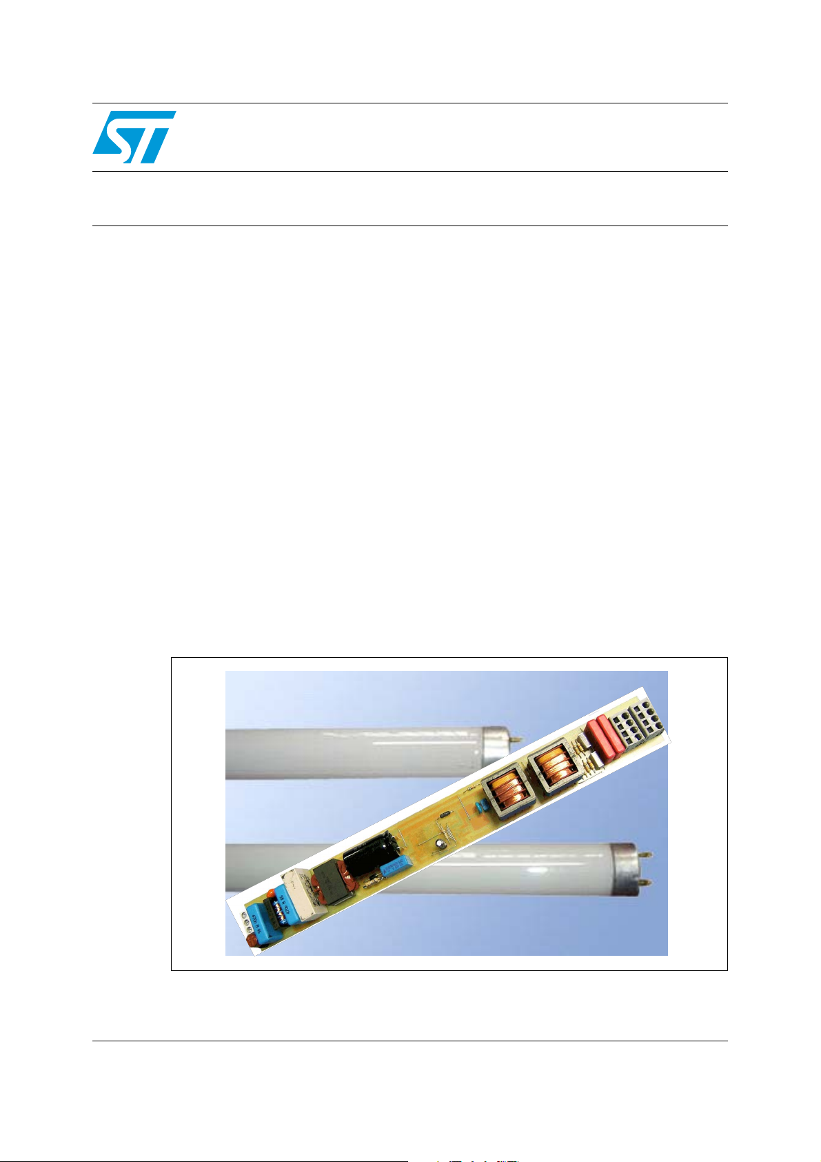
Figure 1. 2x58W T8 ballast demonstration board
August 2008 Rev 1 1/27
www.st.com
Page 2

Contents AN2771
Contents
1 Basis of half-bridge inverter topology . . . . . . . . . . . . . . . . . . . . . . . . . . 4
2 Main characteristics . . . . . . . . . . . . . . . . . . . . . . . . . . . . . . . . . . . . . . . . . 5
3 Ballast design . . . . . . . . . . . . . . . . . . . . . . . . . . . . . . . . . . . . . . . . . . . . . . 7
3.1 L6585D biasing circuitry (pin by pin) . . . . . . . . . . . . . . . . . . . . . . . . . . . . . 7
3.2 PFC power section design . . . . . . . . . . . . . . . . . . . . . . . . . . . . . . . . . . . . 11
3.3 Half-bridge inverter design . . . . . . . . . . . . . . . . . . . . . . . . . . . . . . . . . . . . 12
3.4 Symmetrical and asymmetrical EOL protection: improvements . . . . . . . . 13
4 Experimental results . . . . . . . . . . . . . . . . . . . . . . . . . . . . . . . . . . . . . . . . 16
5 Protections . . . . . . . . . . . . . . . . . . . . . . . . . . . . . . . . . . . . . . . . . . . . . . . . 19
6 Conduction emissions test . . . . . . . . . . . . . . . . . . . . . . . . . . . . . . . . . . 21
6.1 Adapting the design for a 2x36 W T8 electronic ballast . . . . . . . . . . . . . . 21
7 Revision history . . . . . . . . . . . . . . . . . . . . . . . . . . . . . . . . . . . . . . . . . . . 26
2/27
Page 3

AN2771 List of figures
List of figures
Figure 1. 2x58W T8 ballast demonstration board . . . . . . . . . . . . . . . . . . . . . . . . . . . . . . . . . . . . . . . . 1
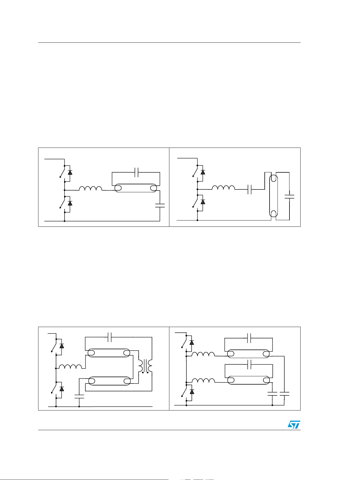
Figure 2. Electronic lamp ballast - capacitor-to-ground configuration . . . . . . . . . . . . . . . . . . . . . . . . . 4
Figure 3. Electronic lamp ballast - lamp-to-ground configuration. . . . . . . . . . . . . . . . . . . . . . . . . . . . . 4
Figure 4. Dual lamp ballast series configuration . . . . . . . . . . . . . . . . . . . . . . . . . . . . . . . . . . . . . . . . . 4
Figure 5. Dual lamp ballast parallel configuration . . . . . . . . . . . . . . . . . . . . . . . . . . . . . . . . . . . . . . . . 4
Figure 6. Electrical schematic 2x58 W T8 . . . . . . . . . . . . . . . . . . . . . . . . . . . . . . . . . . . . . . . . . . . . . . 6
Figure 7. TSM101 window comparator configuration . . . . . . . . . . . . . . . . . . . . . . . . . . . . . . . . . . . . 13
Figure 8. External symmetrical EOL protection . . . . . . . . . . . . . . . . . . . . . . . . . . . . . . . . . . . . . . . . . 14
Figure 9. L6585 startup sequence . . . . . . . . . . . . . . . . . . . . . . . . . . . . . . . . . . . . . . . . . . . . . . . . . . . 17
Figure 10. One lamp ignition phase . . . . . . . . . . . . . . . . . . . . . . . . . . . . . . . . . . . . . . . . . . . . . . . . . . . 17
Figure 11. Low-side current in run mode . . . . . . . . . . . . . . . . . . . . . . . . . . . . . . . . . . . . . . . . . . . . . . 18
Figure 12. Voltage and current lamp in run mode . . . . . . . . . . . . . . . . . . . . . . . . . . . . . . . . . . . . . . . . 18
Figure 13. Asymmetrical EOL protection with broken cathode during run mode. . . . . . . . . . . . . . . . . 19
Figure 14. Symmetrical EOL protection behavior during ignition phase . . . . . . . . . . . . . . . . . . . . . . . 20
Figure 15. Conducted emissions at 230 Vac 50 Hz - line 1 peak detector . . . . . . . . . . . . . . . . . . . . . 21
Figure 16. Conducted emissions at 230 Vac 50 Hz - line 2 peak detector . . . . . . . . . . . . . . . . . . . . . 21
3/27
Page 4
Basis of half-bridge inverter topology AN2771
1 Basis of half-bridge inverter topology
The half-bridge inverter operates in zero voltage switching (ZVS) resonant mode, to reduce
the switching losses and the electromagnetic interference generated by the output wiring
and the lamp. Voltage-fed series resonant half-bridge inverters are currently used for
compact fluorescent lamp ballasts (CFL) and for many European tube lamp (TL) ballasts.
Generally, for lighting applications, considering the current preheating, it's possible to
choose between two different topologies of the resonant circuit: capacitor-to-ground
(Figure 2) or lamp-to-ground (Figure 3).
Figure 2. Electronic lamp ballast - capacitor-
to-ground configuration
Figure 3. Electronic lamp ballast - lamp-to-
ground configuration
+
L
RES
V
dc
C
RES
C
Block
_
In the design presented in this application note, a capacitor-to-ground configuration was
used. For dual lamp ballast the lamps can be connected in series (Figure 4) or in parallel
(Figure 5). In the system presented here, a parallel configuration was chosen for the
following reasons:
● lower voltage stress on the ballast output stage components, on the wiring, and on the
fixture sockets
● the resonant L and C associated with the lamps are less sensitive to component
tolerances due to the lower operating lamp voltages compared to the series
configuration
● better lamp control as it is possible to independently monitor both lamp operations
Figure 4. Dual lamp ballast series
+
configuration
C
RES
+
L
rRES
V
dc
C
Block
_
Figure 5. Dual lamp ballast parallel
configuration
C
+
RES
C
RES
L
rRES
C
-
Block
L
rPRE
4/27
L
rRES
C
-
Block
Page 5

AN2771 Main characteristics
2 Main characteristics
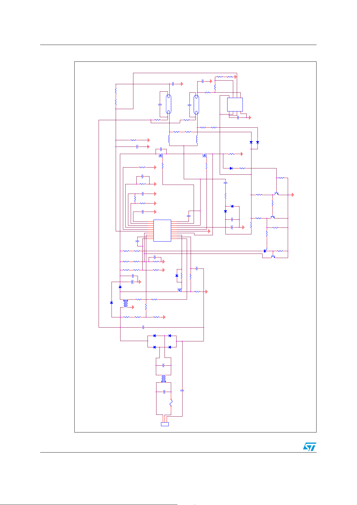
The electrical specifications for the electronic lamp ballast are given in Tab le 1 and the
schematic for the 2x58 W T8 is presented in Figure 6. The ballast design procedure is
detailed in the following section.
Table 1. Input and output parameters
Input parameters
V
IN
f
line
Number 2
Type T8 in parallel configuration
Power 58 W or 36 W
PF Power factor
THD% Total harmonic distortion ≤ 10
η % Efficiency
Input voltage range 185 to 265 V
Line frequency 50/60 Hz
Tube l a mp
Target output parameters
≈ 0.9
≈ 90 %
RMS
5/27
Page 6
Main characteristics AN2771
Figure 6. Electrical schematic 2x58 W T8
R540RR54
0R
10 kOhm
10 kOhm
R26
R26
C15
C15
R25
R25
1.6 kOhm
1.6 kOhm
100 nF, 400V
LAMP2
LAMP2
R53 0R53 0
1
4
L2
R22
R22
23
T8 Lamp1-58W
T8 Lamp1-58W
R40
R40
1.8 mHL21.8 mH
1 5
Q4
R23
R23
C25
CAP NP
C25
CAP NP
0.33 ohm 1% 1W
0.33 ohm 1% 1W
100 nF, 400V
R24
R24
1.802 MOhm
1.802 MOhm
68k
68k
STD8NM60NQ4STD8NM60N
62 Ohm
62 Ohm
7
8
5
6
Vrin
Crin
+Vcc
Output
Vref1Csense2Crref3GND
U2
56k
56k
R41
R41
C16
C16
R29 10 OhmR29 10 Ohm
D8 1N4148D8 1N4148
R31
R31
D13
D13
1 nF 1kV
1 nF 1kV
D9
C17
C17
LL4148
LL4148
16VD916V
C18
C18
4
100 nF
100 nF
C19
C19
0.33 ohm 1% 1W
0.33 ohm 1% 1W
R56
R56
100nF
100nF
4.7uF 50V
4.7uF 50V
TSM101U2TSM101
D12 BAT46ZD12 BAT46Z
D11 BAT46ZD11 BAT46Z
18k
18k
R46
470k
R46
470k
1
Q5
R47
R47
330k
330k
R49
R49
330k
330k
R52 0R52 0
BC847Q5BC847
32
R48 10R48 10
1
Q6
BC847Q6BC847
32
R50
R50
56k
56k
R51 2kR51 2k
2
Q7
XO205MAQ7XO205MA
R55
470
R55
470
1 3
1
32
BC847Q8BC847
Q8
1N4007
1N4007
D10
D10
D2
R4
R3
STTH1L06D2STTH1L06
560 kOhmR4560 kOhm
560 kOhmR3560 kOhm
R27
R27
R7
R6
0.8 mH
0.8 mH
56K
56K
910 kOhmR7910 kOhm
1.5 MOhmR61.5 MOhm
R5
LPFC1
LPFC1
1 MOhmR51 MOhm
C1
C1
1 3
5 8
R13
R13
C2
C21
C21
+
+
R8
C3
30 KOhm
30 KOhm
470//100 nFC2470//100 nF
R30
R30
R12
R12
910 kOhm
910 kOhm
R11
R11
1.5 MOhm
1.5 MOhm
100nF 630V
100nF 630V
47uF 450V
47uF 450V
R320R32
R9
16 kOhmR816 kOhm
33 nFC333 nF
56K
56K
0
390 kOhmR9390 kOhm
C7
R14
R14
240 kOhm
240 kOhm
R15
R15
C6
20 kOhm
20 kOhm
C5
R16
R16
470//220 nFC7470//220 nF
1.2 MOhm
1.2 MOhm
470//150C6470//150
1.8 nFC51.8 nF
R33 0R33 0
1
2
3
4
5
6
7
8
9
10
C8
R10
R10
C9
10 nF 1600VC910 nF 1600V
R34
R34
180k
180k
Q2
U1
L6585DU1L6585D
Osc
RF
EOI
Mult
INV
10 nFC810 nF
R19
R19
R18
R18
18 kOhm
18 kOhm
15 kOhm
15 kOhm
R17
20//11 kOhm
R17
20//11 kOhm
C22
C22
R20
R20
TCH
EOLP
EOL-R
CTR
Comp
13 kOhm
13 kOhm
220 pF 1kV
220 pF 1kV
62 Ohm
62 Ohm
4
LAMP1
LAMP1
1
2 3
L1
1 5
STD8NM60NQ2STD8NM60N
Boot
HSD
Out
VCC
LSD
GND
HBCS
PFG
PFCS
ZCD
C12
C12
T8 Lamp1-58W
T8 Lamp1-58W
1.8 mHL11.8 mH
20
19
18
17
16
15
14
13
12
11
D7
BAT46ZD7BAT46Z
100 nF, 400V
100 nF, 400V
R36
68k
R36
68k
Q3
C14
10 nF 1600V
C14
10 nF 1600V
R35
R35
180k
180k
R37
56k
R37
56k
C13
C13
100nF 50V
100nF 50V
R21
R21
10 Ohm
10 Ohm
STD6NK50ZQ3STD6NK50Z
C4
470 nFC4470 nF
GF1MD6GF1M
D4
GF1MD4GF1M
D6
D5
GF1MD5GF1M
D3
GF1MD3GF1M
C11
100nF 275V X2
C11
100nF 275V X2
43
LPFC2
LPFC2
12
2x39 mH/0.7A
2x39 mH/0.7A
C10
C10
100nF 275V X2
100nF 275V X2
F1 3AF1 3A
213
J1
CON3J1CON3
6/27
C20
C20
1nF 275 VAC Y1
1nF 275 VAC Y1
Page 7

AN2771 Ballast design
3 Ballast design
The design of the major parts of the circuit is described in this section.
3.1 L6585D biasing circuitry (pin by pin)
Designed in high-voltage BCD offline technology, the L6585D embeds a PFC controller, a
half-bridge controller, the relevant drivers and the logic necessary to build an electronic
ballast.
● Pin 1 OSC is one of the two oscillator inputs. The value of the capacitor connected to
ground defines the half-bridge switching frequency in each operating state. A value of
1.8 nF was chosen.
● Pin 2 RF. The component choice with oscillator capacitance defines the half-bridge
switching frequency in each operating state. A resistor R
the run frequency while during preheating the switching frequency is set by the parallel
of R
with R13 connected between pins RF and EOI (short-circuit during preheating).
14
Choosing the following frequencies and ignition time:
connected to ground sets
14
=
run
we can immediately calculate R
kHz39f
with the following formula:
14
pre
=
kHz65f
ign
=
ms60t
Equation 1
and for the value of R
13
14
⋅
Cf
5run
326.1
= k20
R
:
Ω=
Equation 2
R326.1
⋅
PRE
145pre
//R
14
41.1RCf
−⋅⋅
) connected between the RF pin and
RUN
Ω=
R
= k30
13
● Pin 3 EOI is a multifunction pin. During preheating the pin is internally shorted to
ground by the logic, so the resistor (R
ground sets the preheating switching frequency. During ignition pin EOI becomes high
impedance. The ignition time is the time necessary for the pin voltage to exponentially
rise from zero to 1.9 V. The growth is steered by the C
value of R
has already been calculated and t
13
ign
* R13 time constant. As the
6
at start is fixed, the value of C6 is
calculated by the following formula:
Equation 3
t
C
ign
=
6
R3
⋅
13
nF666
=
7/27
Page 8

Ballast design AN2771
The value C6=620 nF was chosen. In order to have this value, two capacitors in parallel
were mounted C
● Pin 4 TCH is the time counter and it is necessary to establish the preheating time and
=470//150 nF.
6
the protection intervention time (either overcurrent or EOL). To implement the time
counter, a R
=690 nF and t
C
7
we can calculate R
parallel network is connected between this pin and ground. Choosing
15C7
=1 sec and considering the internal current generator ICH=34 µA,
pre
as follows:
15
Equation 4
C
7
⋅−
t
pre
= M2.1
R
15
⋅
7
● Pin 5 EOLP is a 2 V reference and allows programming the window comparator of pin 6
63.4
I
CH
lnC
63.4
5.1
Ω=
(EOLR) according to table 5 of the L6585D datasheet. Choosing a reference tracking
with the CTR pin and a window voltage amplitude ± 220 mV, we chose R
● Pin 6 EOLR is the input of both the window comparator and a re-lamp comparator.
=240 kΩ.
16
Concerning the window comparator (choosing tracking with CTR pin), the center is the
same voltage as the CTR pin so the resistive divider connected across the block
capacitor (see C
in Figure 2) is set such that under normal conditions:
block
Equation 5
R
19
()
RRR
++
12719
R
8
()
++
RRR
438
()
RR
+
127
2
⋅=
43
1
+
R
8
V
EOLR
VV
CTREOLR
VV
⇒=
⋅=
BUSpfcCTR
V
BUSpfc
⋅=
2
()
RR
+
R
19
To determine the resistance values of (R7+R12), R19, (R3+R4), R8, decisions concerning
pin 7 CTR are needed.
● Pin 7 CTR is a multifunction pin (PFC overvoltage, feedback disconnection, reference
for EOL in case of tracking reading), connected to a resistive divider to the PFC output
bus. Establishing the maximum PFC overvoltage (PFC output overshoot e.g. at startup)
at V
OVPBUSpfc
pin must be V
= 13 kΩ. From Equation 5, fixing R3+R4 = 1120 kΩ, the following resistance value
R
19
is obtained R
● Pin 8 MULT. Assuming a peak value of V
= 480 V and considering that the correspondent threshold on the CTR
thrCTR
= 16 kΩ.
8
= 3.4 V, we can immediately calculate R7+R
multpkMax
= 1.8 V (at VAC = 265 V) on the
= 1.82 MΩ and
12
multiplier input (MULT, pin 8), the peak value at minimum line voltage is
V
MULTpkmin
= 1.8 × 185/265 = 1.25 V which, multiplied by the maximum slope of the
multiplier, 0.75, gives 0.94 V peak voltage on current sense (CS, pin 4). Since the
linearity limit (1 V) is not exceeded, this is acceptable. Considering about 250 µA
current for the divider, the lower resistor is 7.14 kΩ (20//11 kΩ ). To establish the upper
resistance value (referring to the PFC section of the L6585D datasheet), the ratio
between Vmult and Vin for different input voltage must be evaluated:
8/27
Page 9

AN2771 Ballast design
Equation 6
RRR
9517
inMin
V
=
V2
⋅
inMax
V
CSclamp
slopemax
maxmultPK
=
axmultSlopeM
3
−
108.4
⋅=
1
V2
⋅
inMin
3
−
101.5
⋅=
V
inMin
⇒
R
V
⇒
inMax
R
17
()
RRR
++
9517
17
()
++
V
=
⋅
V2
where:
● V
CSclamp
● max slope is the maximum slope of the multiplier characteristic family for L6585D
● V
multSlopeMax
is the clamp value of the voltage current sense for L6585D
is the maximum voltage in the mult pin with Vin=V
inMin
To work in the linear area of the multiplier characteristic family, the upper resistance choice
is made considering the lowest of ratios calculated in
R
● Pin 9 COMP is the output of the E/A and also one of the two inputs of the multiplier. The
= 1.390 MΩ was mounted.
5+R9
Equation 6 ⇒ R
=1.487 MΩ.
5+R9
feedback compensation network, placed between this pin and INV (10), is simply a
capacitor calculated as follows (considering R
is the upper resistance of the
6+R11
voltage divider between the PFC bus and COMP pin):
Equation 7
C
=
2
10
()
RR2
+⋅π⋅
116
nF530
=
A value of C2=560 nF was chosen.
● Pin 10 INV. To implement the voltage control loop, a resistive divider (Figure 6) is
connected between the regulated output voltage V
pin. The internal reference on the noninverting input of the E/A is 2.5 V, so R
Figure 6) are then selected, establishing a max overvoltage ∆V
(
= 420 V of the boost and the
BUSpfc
OVPBUSpfc
and R
6
= 60 V, as
11
follows:
Equation 8
V
RR
where I
+
R
18
RR
=+ M3
116
18
= 20 µA is the threshold current flowing through the compensation network in
OVPth
116
V
∆
OVPBUSpfc
I
BUSpfc
OVPth
1
−=
5.2
Ω=
Ω⇒Ω=⇒ k18k964.17R
case an abrupt load drop happens.
● Pin 11 ZCD is the input to the zero current detector circuit. The ZCD pin is connected to
the auxiliary winding of the boost inductor through a limiting resistor. The ZCD circuit is
negative-going edge-triggered: when the voltage on the pin falls below 0.7 V, the PWM
latch is set and the MOSFET is turned on. To do so, however, the circuit must first be
armed. Prior to falling below 0.7 V, the voltage on pin 11 must experience a positivegoing edge exceeding 1.4 V (due to the MOSFET's turnoff). The maximum main-to-
9/27
Page 10

Ballast design AN2771
auxiliary winding turn ratio, m, has to ensure that the voltage delivered to the pin during
the MOSFET's OFF-time is sufficient to arm the ZCD circuit.
Then:
Equation 9
m
≤
⋅−
4.1
(max)inRMSBUSpfc
10.33
=
V2V
We chose m=10.
Considering the upper and lower clamp voltage of the ZCD pin, its minimum current sink
current capability, according to the max and min voltage of the PFC bus, we can
immediately calculate and choose R
● Pin12 PFCS is the inverting input of the current sense comparator. As the voltage
= 15 kΩ.
10
across the sense resistor (proportional to the instantaneous inductor current) crosses
the threshold set by the multiplier output, the power MOSFET is turned off. Following
the indication given in AN966, page 13, considering the max peak current absorbed by
two lamps, it is possible to determine the following PFC sense resistor:
Equation 10
22
Ω≤ m340R
We chose R22=330 mΩ with a power rating of 0.5 W.
Considering the clamp value voltage on this pin, V
determine the maximum inductor current I
● Pin13 PFG. To correctly drive the external MOSFET, a resistor R
● Pin 14 HBCS. Establishing during ignition, for each lamp, a maximum current of
I
IGNmax
V
= 2.5 A and considering the HBCS threshold during ignition phase
HBCS-ign
= 1.6 V, we can calculate R
Lmax
senseHB=R31
CSclamp
= 3.5 A.
= 1.16 V, it was possible to
=10 Ω was used.
21
:
Equation 11
V
ignHBCS
R
31
−
I
TOTmaxIGN
Ω==
32.0
We chose R31 = 0.33 Ω.
● Pin 15 GND: ground
● Pin 16 LSD. To correctly drive the external half-bridge low-side MOSFET, a resistor
R
=62 Ω was used.
23
● Pin 17 Vcc. This pin is externally connected to the startup circuit (by means of R
R
, R40, R41) and to the self-supply circuit consisting of a charge pump composed of
37
the net C
● Pin 18 Out: high-side driver floating reference. This pin is connected close to the
, C17, C18, D8, D9, R29.
16
34
, R35,
source of the high-side power MOSFET.
● Pin 19 HSD. To correctly drive the external half-bridge low-side MOSFET a resistor
R
=62 Ω was used.
20
● Pin 20 Boot. For the high-side section a C
= 100 nF was selected.
boot
10/27
Page 11

AN2771 Ballast design
(
)
3.2 PFC power section design
Input capacitor
The input high-frequency filter capacitor C4 has to attenuate the switching noise due to the
high-frequency inductor current ripple. The worst conditions occur on the peak of the
minimum rated input voltage V
● the coefficient of maximum high frequency voltage ripple r = 0.05
● total system efficiency is possible, considering the minimum half-bridge switching
frequency f
= 39 kHz and the total output power P
swmin
determine the input capacitor C
Equation 12
C
C4=470 nF was chosen.
Output capacitor
The output bulk capacitor C1 selection depends on the DC output voltage, the admitted
overvoltage, the output power and the desired voltage ripple where:
● PFC output voltage V
● the coefficient of low-frequency (twice the mains frequency f
r
= 0.05
1
We can calculate the bulk capacitor in
busPFC
= 185 V where:
inmin
as follows:
4
=
4
= 420 V
P
outTOT
V
⋅η
minin
mininminsw
Equation 13:
= 2*58 = 116 W, to
outTOT
nF307
=
rVf2
⋅⋅⋅π⋅
= 50 Hz ) voltage ripple
min
Equation 13
P
outTOT
V
=
C
1
busPFC
rVf22
⋅⋅⋅π
1busPFCmain
F21
µ=
To have the smallest ripple and good reliability, we chose capacitor C1 =47 µF, 450 V.
Boost inductor
The inductance L
is greater than the maximum frequency of the internal starter in order to ensure a correct TM
operation. Considering the minimum suggested value for the PFC section f
and that it can occur at the either the maximum V
V
inrmsMin
= 185 V mains voltage, the inductor value is defined by:
Equation 14
To obtain a margin from f
the inductor is determined by V
stated in the PFCS pin description, a maximum current I
is usually determined so that the minimum switching frequency f
pfc
min pfc
L
min pfc
2
inrms
=
pfc
we chose f
= V
inrms
inrmsMax
P
f2
inrmsMax
out
⋅⋅
pfcmin
η
= 33 kHz. In this condition the lower value for
pfc
and L
= 265 V or the minimum
V2VV
⋅−⋅
inrmsbusPFC
V
⋅
busPFC
= 0.8 mH with, as previously
pfc
= 3.5 A.
Lmax
min pfc
= 20 kHz
11/27
Page 12

Ballast design AN2771
Power MOSFET
The choice of the MOSFET concerns mainly its R
, which depends on the output
DS(on)
power, and its breakdown voltage. This last voltage is fixed just by the output voltage
V
= 420 V, plus the overvoltage ∆V
buspfc
= 60 V allowed and a safety margin.
OVPpfc
The MOSFET's power dissipation depends on the conduction and switching losses.
Establishing maximum total power losses P
lossesAdm
= 1% and P
= 1.16 W, it is easy to
outTOT
verify that in choosing SuperMesh power MOSFET STD6NK50Z, the estimated total
MOSFET power losses, in the worst case, is about P
lossesEst
= 0.6 W, so this choice was the
definitive one.
Boost diode
The boost freewheeling diode is a fast recovery one. The breakdown voltage is fixed with the
same criterion as the MOSFET. The values of its DC and RMS current, which are needed to
choose the current rating of the diode, are given as follows:
Equation 15
P
I
outTOT
BUSpfc
⋅⋅=
==
24
9
π
dc2D
V
I22I
rmsrms2D
Since the PFC works in transition mode, the Turbo 2 Ultrafast high-voltage rectifier
STTH1L06 was selected.
V
inrms
V
BUSpfc
A276.0
A6.0
=⋅
3.3 Half-bridge inverter design
Concerning the resonant circuit design, according the criteria described in AN993 section 5,
we chose the following:
●
●
●
The P-Mos selection in the half-bridge section is performed mainly considering the max
power losses admitted on each switch P
current through it IrmsMOS ≅ 0.6 A. Concerning half-bridge devices, using the second
generation MDmesh Power MOSFET STD8NM60N, the estimated power losses in it result
in P
lossesEstHB
≅ 0.468 W.
===
21res
===
149res
===
1512block
lossesAdm1
mH8.1LLL
= 0.5% P
V1600/nF10CCC
V400/nF100CCC
≅ 0.6 W and the rms
outTOT
12/27
Page 13
AN2771 Ballast design
3.4 Symmetrical and asymmetrical EOL protection: improvements
As previously stated, the L6585D includes two functions concerning EOL protections which
are summarized as follows:
a) The first function has been designed to detect the ageing of the lamp with
particular attention to the effect appearing as asymmetric rectification. The idea is
to measure the variation of the DC component of the lamp voltage that can be
either positive or negative. A window comparator has been introduced (centered
around Vref with amplitude "V
than V
two standard ballast configurations (lamp-to-ground and block capacitor-toground).
b) Concerning the second function, as soon as a fault due to broken lamp in ignition
mode (1.6 V threshold crossing) or a symmetrical EOL in run mode (0.9 V
threshold crossing) triggers the TCH timer, the frequency control starts. When the
timer ends, the current is monitored on the HBCS pin at the first cycle. In both
conditions if the HBCS threshold is still crossed, the oscillator stops, the chip
enters low-consumption mode /shutdown mode and this condition is latched until
the mains supply is removed or re-lamp is detected.
The following improvements in the protection functions have been implemented:
– The asymmetric rectification protection, described above, was implemented to
monitor the status of only one lamp. To protect the second lamp with the same
criteria (voltage window comparator) as the first one, a voltage and current control
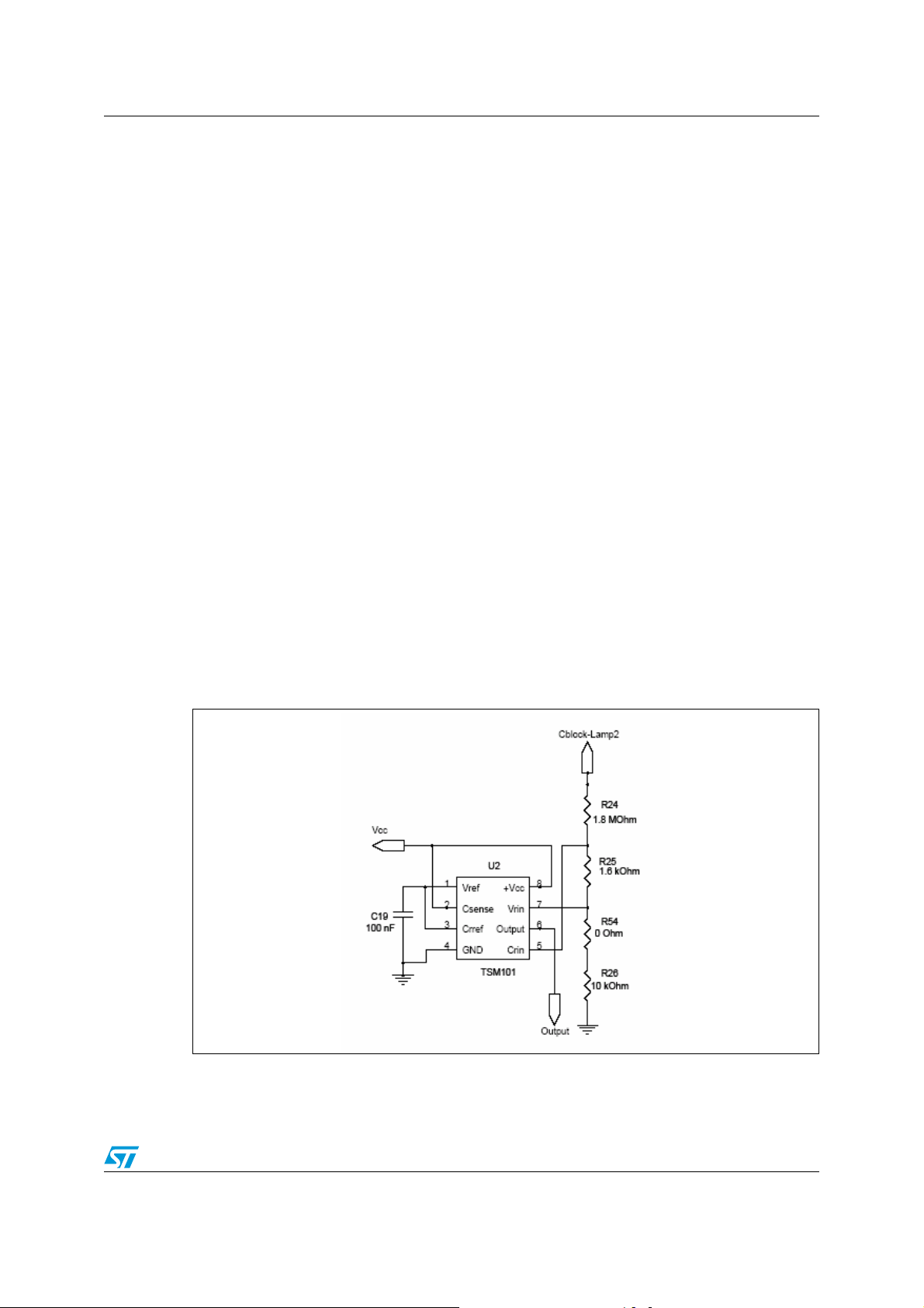
TSM101 in the configuration shown in
possible to obtain the asymmetric rectification protection in a reliable and
independent manner for each lamp.
+ Vw/2 or lower than Vref- Vw/2. This kind of protection is compliant to the
set
") that triggers when the EOL-R voltage is higher
w
Figure 7 was used. With this circuit it was
Figure 7. TSM101 window comparator configuration
The design criteria for TSM101 in window comparator configuration is described in the
following paragraphs. By means of a voltage divider R
, R25, R54+R26, from the block
24
13/27
Page 14

Ballast design AN2771
capacitor of the second lamp, TSM101 checks that the average voltage value on the
capacitor is V
Considering that the voltage window used for the first lamp is ∆V
15%V
, for the second lamp a similar percent voltage window ∆V
CTR
AVE
= 210 V.
window1
window2
= 2*220 mV ≅
≅ 15%V
AVE
=
31 V was chosen. Establishing the second voltage window and considering that the voltage
reference in TSM101 is V
= 1.24 V, it is easy to calculate the resistance value of the
ref
voltage divider mentioned in the previous paragraph (presuming, in normal conditions, an
absorbed current in it of I
Vdivider
≅ 116 µA ) as follows:
Equation 16
V
RRRRR
26542524tot
R
AVE
−
tot
∆
V
+
⎛
V
⎜
AVE
⎝
⋅+−
∆
V
R
tot
2window
2
∆
V
−
2
R
tot
⎞
2window
⎟
2
⎠
⋅=+ k10RR9954
VRR
ref2654
V
()
RRV
2654ref
= k6.1R1540
R
25
⎛
V
⎜
AVE
⎝
AVE
I
Vdivider
⎞
2window
⎟
⎠
Ω==+++= M81.1
2654
25
Ω=+⇒Ω=
Ω=⇒Ω=
265425tot24
Ω⇒Ω=++−= M8.1M798.1)RRR(RR
– The symmetrical EOL protection described in paragraph b of this section was
improved because for a two-lamp application an event such as the breaking of one
lamp and the ignition of the other one may not activate the embedded device
protection quickly enough.
To avoid this type of issue and in order to increase the reliability of the protection, an
external circuit as shown in
Figure 8 was implemented.
Figure 8. External symmetrical EOL protection
14/27
Page 15

AN2771 Ballast design
This circuit (considering that it is possible to latch the device maintaining the CTR pin to zero
voltage), by means of an inverting logic made by Q
the half-bridge current sense resistor V
. Overcoming a fixed voltage threshold on the HB
R31
current sense, the X0205MA SCR is activated which consequently activates Q
and Q6, is activated by the voltage on
5
and causes
8
the CTR pin to go down to zero voltage. The device is latched until the main supply is
removed.
15/27
Page 16

Experimental results AN2771
4 Experimental results
The schematic of the tested board is shown in Figure 6 . The board was first tested in terms
of efficiency, power factor, total harmonic distortion and thermal behavior for the input
voltage range.
Table 2. 2x58 W T8 board performance
Ta bl e 2 and Tab le 3 show the results obtained for testing during 45 minutes.
V
IN
(V)
185 115.5 52 0.90 0.645 0.995 7.9
230 112.5 52 0.92 0.515 0.992 8
265 113.5 52 0.91 0.455 0.988 10
P
IN
(W)
P
OUTlamp1
(W)
I
η
(A)
IN
PF
THD
(%)
All results obtained are very good. Efficiency is about 90%, the power factor corrector is
constantly 0.99, and THD is about 8%.
Table 3. 2x58 W T8 thermal results of critical system components
V
(V) Ambient temp (°C)
IN
1852371795849
2302371794747
2652371784447
Temp MO S
LowSide
(°C)
Concerning thermal behavior, from the results given in
Tem p MOS
(°C)
HighSide
Temp MO S
(°C) Temp L6585D (°C)
PFC
Ta bl e 3 , it is easy to deduce,
considering the highest ambient temperature, that there is a good safety margin from the
max junction temperature of the MOS.
Startup sequence
Figure 9 shows the startup sequence: the IC supply voltage V
bridge starts oscillating and starts the charge capacitor connected to TCH. When the
voltage at the TCH pin reaches VCHP (4.63 V), the same capacitor is discharged following
an exponential decrease steered by the time constant, which defines the preheating time.
During this time, the EOI pin is forced to ground and the switching frequency is set by the
oscillator at the preheating value. When the voltage at the TCH pin drops down to 1.53 V,
the EOI pin is exponentially charged according to a time constant that defines the ignition
time. At the same time the TCH pin goes down to ground. During this phase the oscillator
generates a reduction of the switching frequency. As the voltage at EOI exceeds 1.9 V, the
chip enters run mode.
16/27
reaches V
CC
CCon
, the half-
Page 17

AN2771 Experimental results
Figure 9. L6585 startup sequence
Figure 10
shows the lamp ignition phase. The voltage across it increases linearly as well as
the current flowing through it.
Figure 10. One lamp ignition phase
17/27
Page 18

Experimental results AN2771
Figure 11. Low-side current in run mode
Figure 12. Voltage and current lamp in run mode
18/27
Page 19
AN2771 Protections
5 Protections
As previously stated in Section 3.4, due to the presence of two lamps, TSM101 must be
added to implement the asymmetric EOL protection, and inverter logic with a SCR must be
added to implement the symmetrical EOL protection. The following failures were simulated
to test these:
● Cathode breaking in run mode
● Broken tube or failure to strike during ignition phase
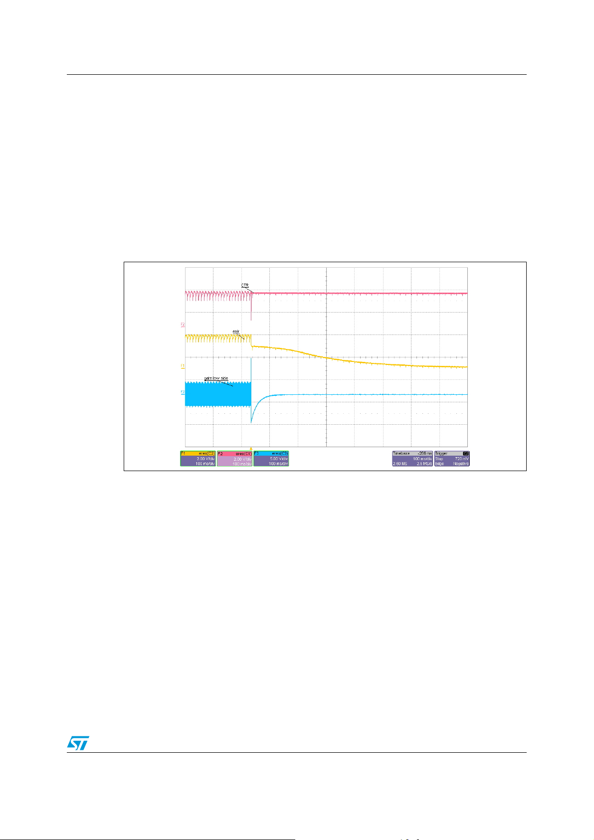
As shown in Figure 13, as soon as a cathode of one lamp is broken, the voltage on the
EOLR pin goes out from the valid voltage window and the L6585D stops switching.
Figure 13. Asymmetrical EOL protection with broken cathode during run mode
When one of the two lamps is broken or the the gas inside is exhausted, during the ignition
phase, as illustrated in Figure 14, the right lamp is ignited normally, but the voltage across
the broken lamp rises up continually until an established threshold is exceeded that
activates the SCR, by means of an inverter logic, and moves the CTR pin down to ground. In
this condition the L6585D is latched.
19/27
Page 20

Protections AN2771
Figure 14. Symmetrical EOL protection behavior during ignition phase
20/27
Page 21

AN2771 Conduction emissions test
z
W
6 Conduction emissions test
Conducted emissions have been measured in neutral and line wires using peak detector
and considering the limits for lighting applications i.e. EN55015. The measurements have
been performed at 230 Vac line. The results are shown in
the emission level is below both the quasi-peak and average limits with an acceptable
margin, the power supply passes the precompliance test.
Figure 15. Conducted emissions at 230 Vac 50 Hz - line 1 peak detector
Figure 15 and Figure 16. Since
V
µ
AA
02:15:56 Feb 11, 2008
Atte n 0 dB
Mkr1 22.03 MH
30.66 dB
1
Sweep 881.3 ms (2115 pts)
Stop 3 0 M Hz
V
µ
Ref 75 dB
Peak
Log
10
dB/
W1 S2
S3 FC
Start 150 kHz
Res BW 9 kHz VBW 30 kHz
Figure 16. Conducted emissions at 230 Vac 50 Hz - line 2 peak detector
Ref 75 dB
Peak
Log
10
dB/
02:21:25 Feb 11, 2008
V
µ
Atte n 0 dB
Cntr1 22.034 MHz
31.67 dB
Marker Count: Widen Res B
1
V
µ
W1 S2
S3 FC
AA
Start 150 kHz
Res BW 9 kHz VBW 30 kHz
Sweep 881.3 ms (2115 pts)
Stop 3 0 M Hz
6.1 Adapting the design for a 2x36 W T8 electronic ballast
Using a developed design for 2x58 W T8 tubes, it was possible to do some simple
adjustments to adapt the same design for 2x36 W T8 tubes. Using the same resonant
21/27
Page 22

Conduction emissions test AN2771
circuit, the adjustments concern only the operating frequencies of the lamp, setting the
following ones at:
kHz65f
run
kHz49f
=
preh
=
we can immediately calculate, by means of Equation 1 and Equation 2, the following value
resistances:
14
Ω= k15R
13
Ω= k47R
In addition a new calibration for the symmetric end-of-life operation is needed, changing the
following resistance to:
56
Ω= 75R
Testing the board with these modifications the experimental results are given below in
Ta bl e 4 :
Table 4. 2x36W T8 board performance
V
(V) P
IN
185 74 33 0.89 0.39 0.994 6.9
230 73.5 33 0.89 0.315 0.987 7.6
(W) P
IN
OUTlamp1
(W) η I
(A) PF THD (%)
IN
265 73.4 33 0.89 0.275 0.979 8.7
Table 5. Bill of material
Item Qty Ref. Part/value
1 1 C1 47 µF, 098 A 20% 450 V
21 C2
3 1 C3 33 nF 5% 50 V
4 1 C4 470 nF 10% 630 V
5 1 C5 1.8 nF 5% 50 V
61 C6
71 C7
81 C8
560 nF
(470//100
nF)
660 nF
(470//150)
nF- ceramic
680 nF
(470//220)
nF-ceramic
10 nF-
ceramic-
Tol er anc e
Volt a g e -
(%)
5% 50 V
5% 50 V
5% 50 V
5% 50 V
current
Watt
Techn ology
information
Electrolytic
capacitor
COG ceramic
capacitor
COG ceramic
capacitor
Polyester
capacitor
COG ceramic
capacitor
COG ceramic
capacitor
COG ceramic
capacitor
COG ceramic
capacitor
Package
footprint
SMD 0805
SMD 0806
Radial 22.5
mm lead
spacing
SMD 0805
SMD 0805
SMD 0805
SMD 0805
Manu-
facturer
EPCOS B43858C5476M
EPCOS
Manufacturer
B32523Q8474K
code
000
000
RS/
distrelec
/other
code
22/27
Page 23

AN2771 Conduction emissions test
Table 5. Bill of material (continued)
RS/
distrelec
/other
code
Item Qty Ref. Part/value
Tol er anc e
(%)
Volt a g e -
current
Watt
Techn ology
information
Package
footprint
Manu-
facturer
Manufacturer
code
9 2 C9, C14 10 nF 5% 1600 V
10 2 C10,C11 100 nF 10% 300 Vac
100 nF,
11 2 C12, C15
12 1 C13
13 1 C16 1 nF 5% 630 V
14 1 C17 4.7 µF 20% 50 V
15 2 C18, C19
16 1 C20 1 nF Y1 20% 250 Vac
17 1 C21 100 nF 10% 630 V
18 1 C22
19 1 C25 Not mounted
20 3
21 1 D2 STTH1L06
22 4
23 2 D8, D13 LL4148
24 1 D9 16 V 5% 16 V
25 1 D10 1N4007
26 1 F1 3,15 A 250 V
27 1 J1 CON3
28
D7,D11,
D12
D3,D4,
D5,D6
Lamp,
Lamp2
400 V-
polyester-
lead spacing
10mm
100 nF-
50V- 10%
100 nFceramic
220 pF -
ceramic-
lead spacing
5 mm
BAT46 150 mA
GF1M-1A
T8 Lamp1-
58 W
10% 400 V
10% 50 V
5% 50 V
10% 1 kV
1000 V 1
75 V 150
A
mA
1000 V
1 A
250V
Metallized
polypropylene
film capacitors
X2
polypropylene
capacitor
Metallized
polyester film
capacitors
Ceramic
capacitor
Polypropylene
capacitor
Electrolytic
capacitor
COG Ceramic
capacitor
Y1 Ceramic
capacitor
polypropylene
capacitor
Ceramic disc
capacitor
Small signal
Schottky
diode
Ultrafast high
voltage
rectifier
Rectifier diode
Switching
diode
500
Zener diodes
mW
Rectifier diode DO-41
TR5 quick
acting submin
PCB F fuse
3 way screw
terminal block
7.5 mm pitch
4 pins PCB
terminal strip
Radial
22.5mm lead
spacing
Radial
10mm lead
spacing
SMD 1206
Radial 5mm
lead spacing
Cylindrical
2.5 mm lead
spacing
SMD 0805
Radial 9.5
mm lead
spacing
Radial 15
mm lead
spacing
Radial 5mm
lead spacing
SMD SOD-
323
DO-41
SMD
DO214BA
SMD SOD-
80
SMD SOD-
123
RADIAL
THT 7.5 mm
lead spacing
THT 5 mm
lead spacing
EPCOS
EPCOS
EVOX
RIFA
CERA
MITE
EPCOS B32652A6104K
Panasonic
STMicro-
electronics
STMicro-
electronics
WAGO
(www.
wago.it)
B32653A1103J
000
B32561J6104K
000
PFR5
102J630J11L4
440LD10-AD
10PCM
ECKA3A221KBPRS: 473-
BAT46JFILM
STTH1L06
739-104
RS: 441-
9616
RS: 240-
4836
RS: 214-
5896
RS: 190-
8371
0373
RS: 269-
451
RS: 447-
1838
RS: 226-
6549
RS: 548-
7317
23/27
Page 24

Conduction emissions test AN2771
Table 5. Bill of material (continued)
Item Qty Ref. Part/value
1
29
Note
30 1 LPFC2
31
Note
32 3
33 2 Q2, Q4
34 1 Q3 STD6NK50Z
35 1 Q7 X0205MA
36 2 R3, R4 560 kΩ 1% 1/4 W
37 1 R5, 1 MΩ 1% 1/4 W
38 2 R7, R12 910 kΩ 1% 1/4 W
39 2 R6, R11 1.5 MΩ 1% 1/4 W
40 1 R8 16 kΩ 1% 1/8 W
41 1 R9 390 kΩ 1% 1/4 W
42 1 R10 15 kΩ 5% 1/4 W
43 1 R13 30 KΩ 1% 1/8 W
44 1 R14 20 kΩ 1% 1/8 W
45 1 R15 1.2 MΩ 1% 1/8 W
46 1 R16 240 k
47 1 R17
48 1 R18 18 kΩ 1% 1/4 W
49 1 R19 13 kΩ 1% 1/4 W
50 2 R20, R23 62 Ω 1% 1/8 W
51 2
52 1 R29 10 Ω 1% 1/4 W
LPFC1 0.8 mH
(1)
2
L1, L2
(1)
Q5, Q6,
Q8
R21,
R48
2x39 mH/0.7
1.8 mH +/5%
BC847 100 mA
STD8NM60
20//11 kΩ -
parallelo-
10 Ω 1% 1/8 W
Tol er anc e
A
N
Ω 1% 1/8 W
Volt a g e -
(%)
5%
1% 1/4 W
current
6 0 0 V
500 V
600 V
0.050
Watt
7 A
6 A
mA
Techn ology
information
Common
mode choke
NPN
transistor
MDmesh™
Powe r
MOSFET
Supermesh
MOSFET
SCRs TO92
Metal film
resistor
Metal film
resistor
Metal film
resistor
Metal film
resistor
Metal film
resistor
Metal film
resistor
Carbon film
resistor
Metal film
resistor
Metal film
resistor
Metal film
resistor
Metal film
resistor
Metal film
resistor
Metal film
resistor
Metal film
resistor
Metal film
resistor
Metal film
resistor
Metal film
resistor
SMD SOT-23
Package
footprint
SMD DPAK
SMD DPAK
SMD 1206
SMD 1206
SMD 1206
SMD 1206
SMD 0805
SMD 1206
axial
SMD 0805
SMD 0805
SMD 0805
SMD 0805
SMD 1206
SMD 1206
SMD 1206
SMD 0805
SMD 0805
SMD 1206
Manu-
facturer
EPCOS
STMicro-
electronics
STMicro-
electronics
STMicro-
electronics
Manufacturer
code
B82732R2701B
030
STD8NM60N
STD6NK50Z
X0205MA
RS/
distrelec
/other
code
24/27
Page 25

AN2771 Conduction emissions test
Table 5. Bill of material (continued)
RS/
distrelec
/other
code
Item Qty Ref. Part/value
Tol er anc e
(%)
Volt a g e -
current
Watt
Techn ology
information
Package
footprint
Manu-
facturer
Manufacturer
code
53 2 R22, R31 0.33 Ω 1% 1W
54 1 R24 1.8 MΩ 1% 1/4 W
55 1 R25 1.6 kΩ 1% 1/4 W
56 1 R26 10 kΩ 1% 1/4 W
57 4
58 1 R50 56 kΩ 1% 1/8 W
59 3
60 2 R53, R54 0 Ω jumper SMD 0805
61 2 R34,R35 180 kΩ 1% 1/4 W
62 2 R36,R40 68 kΩ 5% 1/4 W
63 1 R46 470 kΩ 1% 1/8 W
64 2 R47,R49 330 kΩ 1% 1/8 W
65 1 R51 2 kΩ 1% 1/8 W
66 1 R55 470 Ω 1% 1/8 W
67 1 R56 18 kΩ 1% 1/4 W
68 1 U1 L6585D
69 1 U2 TSM101
70 15 JUMP
71 4 Spacer
R27,R3,
R37,R41
R32,R33,
R52
56 kΩ 5% 1/4 W
0 Ω jumper SMD 1206
Insulate
wire- jump
Note
Spacer/
distanziatori
Wire 0.6
(2)
mm
10 mm Nylon
Precision wire
resistors
Metal film
resistor
Metal film
resistor
Metal film
resistor
Carbon film
resistor
Metal film
resistor
Metal film
resistor
Carbon film
resistor
Metal film
resistor
Metal film
resistor
Metal film
resistor
Metal film
resistor
Metal film
resistor
Combo IC for
PFC and
ballast control
Voltage and
current
controller
Wire 0.6 mm
axial
SMD 1206
SMD 1206
SMD 1206
axial
SMD 0805
SMD 1206
axial
SMD 0805
SMD 0805
SMD 0805
SMD 0805
SMD 1206
SMD SO-20
SMD SO-8
1. Nostra Fornitura max 50 pcs
2. The wire-jump must be insulated
STMicro-
electronics
STMicro-
electronics
Distrele:
720643
L6585D
TSM101AIDT
25/27
Page 26

Revision history AN2771
7 Revision history
Table 6. Document revision history
Date Revision Changes
06-Aug-2008 1 Initial release
26/27
Page 27

AN2771
Please Read Carefully:
Information in this document is provided solely in connection with ST products. STMicroelectronics NV and its subsidiaries (“ST”) reserve the
right to make changes, corrections, modifications or improvements, to this document, and the products and services described herein at any
time, without notice.
All ST products are sold pursuant to ST’s terms and conditions of sale.
Purchasers are solely responsible for the choice, selection and use of the ST products and services described herein, and ST assumes no
liability whatsoever relating to the choice, selection or use of the ST products and services described herein.
No license, express or implied, by estoppel or otherwise, to any intellectual property rights is granted under this document. If any part of this
document refers to any third party products or services it shall not be deemed a license grant by ST for the use of such third party products
or services, or any intellectual property contained therein or considered as a warranty covering the use in any manner whatsoever of such
third party products or services or any intellectual property contained therein.
UNLESS OTHERWISE SET FORTH IN ST’S TERMS AND CONDITIONS OF SALE ST DISCLAIMS ANY EXPRESS OR IMPLIED
WARRANTY WITH RESPECT TO THE USE AND/OR SALE OF ST PRODUCTS INCLUDING WITHOUT LIMITATION IMPLIED
WARRANTIES OF MERCHANTABILITY, FITNESS FOR A PARTICULAR PURPOSE (AND THEIR EQUIVALENTS UNDER THE LAWS
OF ANY JURISDICTION), OR INFRINGEMENT OF ANY PATENT, COPYRIGHT OR OTHER INTELLECTUAL PROPERTY RIGHT.
UNLESS EXPRESSLY APPROVED IN WRITING BY AN AUTHORIZED ST REPRESENTATIVE, ST PRODUCTS ARE NOT
RECOMMENDED, AUTHORIZED OR WARRANTED FOR USE IN MILITARY, AIR CRAFT, SPACE, LIFE SAVING, OR LIFE SUSTAINING
APPLICATIONS, NOR IN PRODUCTS OR SYSTEMS WHERE FAILURE OR MALFUNCTION MAY RESULT IN PERSONAL INJURY,
DEATH, OR SEVERE PROPERTY OR ENVIRONMENTAL DAMAGE. ST PRODUCTS WHICH ARE NOT SPECIFIED AS "AUTOMOTIVE
GRADE" MAY ONLY BE USED IN AUTOMOTIVE APPLICATIONS AT USER’S OWN RISK.
Resale of ST products with provisions different from the statements and/or technical features set forth in this document shall immediately void
any warranty granted by ST for the ST product or service described herein and shall not create or extend in any manner whatsoever, any
liability of ST.
ST and the ST logo are trademarks or registered trademarks of ST in various countries.
Information in this document supersedes and replaces all information previously supplied.
The ST logo is a registered trademark of STMicroelectronics. All other names are the property of their respective owners.
© 2008 STMicroelectronics - All rights reserved
STMicroelectronics group of companies
Australia - Belgium - Brazil - Canada - China - Czech Republic - Finland - France - Germany - Hong Kong - India - Israel - Italy - Japan -
Malaysia - Malta - Morocco - Singapore - Spain - Sweden - Switzerland - United Kingdom - United States of America
www.st.com
27/27
 Loading...