

Page 1
AN2761
Application note
Solution for designing a transition mode
PFC preregulator with the L6562A
Introduction
The TM (transition mode) technique is widely used for power factor correction in low and
middle power applications, such as lamp ballasts, high-end adapters, flat TVs and monitors,
and PC power supplies. The L6562A is the latest proposal from STMicroelectronics for this
market as well as emerging markets that may require a low-cost power factor correction.
Based on a well-established architecture, the L6562A offers excellent performance that
considerably enlarges its field of application.
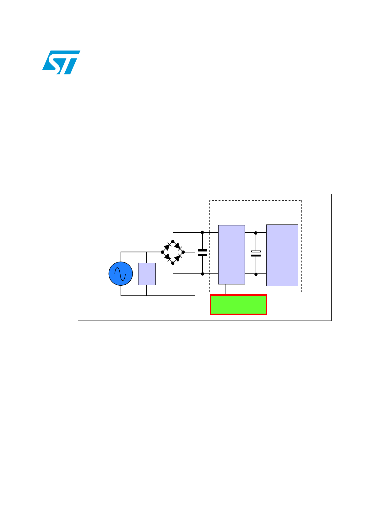
Figure 1. L6562A PFC controller in an SMPS architecture
SMPS
400 VDC
Cin
PFC
CONV.
DC-DC
EMI
filter
PFC controller:
L6562A
November 2009 Doc ID 14690 Rev 2 1/36
www.st.com
Page 2

Contents AN2761
Contents
1 Introduction to power factor correction . . . . . . . . . . . . . . . . . . . . . . . . . 4
2 TM PFC operation (boost topology) . . . . . . . . . . . . . . . . . . . . . . . . . . . . 5
3 Designing a TM PFC . . . . . . . . . . . . . . . . . . . . . . . . . . . . . . . . . . . . . . . . . 7
3.1 Input specification . . . . . . . . . . . . . . . . . . . . . . . . . . . . . . . . . . . . . . . . . . . . 7
3.2 Operating condition . . . . . . . . . . . . . . . . . . . . . . . . . . . . . . . . . . . . . . . . . . 9
3.3 Power section design . . . . . . . . . . . . . . . . . . . . . . . . . . . . . . . . . . . . . . . . 10
3.3.1 Bridge rectifier . . . . . . . . . . . . . . . . . . . . . . . . . . . . . . . . . . . . . . . . . . . . 10
3.3.2 Input capacitor . . . . . . . . . . . . . . . . . . . . . . . . . . . . . . . . . . . . . . . . . . . . 11
3.3.3 Output capacitor . . . . . . . . . . . . . . . . . . . . . . . . . . . . . . . . . . . . . . . . . . 11
3.3.4 Boost inductor . . . . . . . . . . . . . . . . . . . . . . . . . . . . . . . . . . . . . . . . . . . . 12
3.3.5 Power MOSFET selection and dissipation . . . . . . . . . . . . . . . . . . . . . . . 14
3.3.6 Boost diode selection . . . . . . . . . . . . . . . . . . . . . . . . . . . . . . . . . . . . . . . 17
3.4 L6562A biasing circuitry . . . . . . . . . . . . . . . . . . . . . . . . . . . . . . . . . . . . . . 18
4 Design example using the L6562A-TM PFC Excel spreadsheet . . . . . 25
5 EVL6562A-TM-80W demonstration board . . . . . . . . . . . . . . . . . . . . . . . 27
6 Test results and significant waveforms . . . . . . . . . . . . . . . . . . . . . . . . 29
7 L6562A layout hints . . . . . . . . . . . . . . . . . . . . . . . . . . . . . . . . . . . . . . . . 33
8 Reference . . . . . . . . . . . . . . . . . . . . . . . . . . . . . . . . . . . . . . . . . . . . . . . . . 34
9 Revision history . . . . . . . . . . . . . . . . . . . . . . . . . . . . . . . . . . . . . . . . . . . 35
2/36 Doc ID 14690 Rev 2
Page 3

AN2761 List of figures
List of figures
Figure 1. L6562A PFC controller in an SMPS architecture . . . . . . . . . . . . . . . . . . . . . . . . . . . . . . . . . 1
Figure 2. Boost converter circuit . . . . . . . . . . . . . . . . . . . . . . . . . . . . . . . . . . . . . . . . . . . . . . . . . . . . . 5
Figure 3. Inductor current waveform and MOSFET timing. . . . . . . . . . . . . . . . . . . . . . . . . . . . . . . . . . 6
Figure 4. Switching frequency fixing the line voltage . . . . . . . . . . . . . . . . . . . . . . . . . . . . . . . . . . . . . 14
Figure 5. Transition angle versus input voltage . . . . . . . . . . . . . . . . . . . . . . . . . . . . . . . . . . . . . . . . . 16
Figure 6. Capacitive losses . . . . . . . . . . . . . . . . . . . . . . . . . . . . . . . . . . . . . . . . . . . . . . . . . . . . . . . . 16
Figure 7. Conduction losses and total losses in the STP8NM50 MOSFET for the 80W TM PFC . . . 17
Figure 8. L6562A internal schematic . . . . . . . . . . . . . . . . . . . . . . . . . . . . . . . . . . . . . . . . . . . . . . . . . 18
Figure 9. Bode plot - open-loop transfer function. . . . . . . . . . . . . . . . . . . . . . . . . . . . . . . . . . . . . . . . 20
Figure 10. Bode plot - phase . . . . . . . . . . . . . . . . . . . . . . . . . . . . . . . . . . . . . . . . . . . . . . . . . . . . . . . . 20
Figure 11. Multiplier characteristics family . . . . . . . . . . . . . . . . . . . . . . . . . . . . . . . . . . . . . . . . . . . . . . 22
Figure 12. Optimum MOSFET turn-on . . . . . . . . . . . . . . . . . . . . . . . . . . . . . . . . . . . . . . . . . . . . . . . . . 24
Figure 13. Excel spreadsheet design specification input table . . . . . . . . . . . . . . . . . . . . . . . . . . . . . . 25
Figure 14. Other design data . . . . . . . . . . . . . . . . . . . . . . . . . . . . . . . . . . . . . . . . . . . . . . . . . . . . . . . . 25
Figure 15. Excel spreadsheet TM PFC schematic. . . . . . . . . . . . . . . . . . . . . . . . . . . . . . . . . . . . . . . . 26
Figure 16. Excel spreadsheet BOM - 80 W TM PFC based on L6562A . . . . . . . . . . . . . . . . . . . . . . . 26
Figure 17. EVL6562A-TM-80W demonstration board . . . . . . . . . . . . . . . . . . . . . . . . . . . . . . . . . . . . . 27
Figure 18. Wide range 80W demonstration board electrical circuit (EVL6562A-TM-80W) . . . . . . . . . 27
Figure 19. EVL6562A-TM-80W compliance to EN61000-3-2 standard . . . . . . . . . . . . . . . . . . . . . . . . 29
Figure 20. EVL6562A-TM-80W compliance to JEIDA-MITI standard . . . . . . . . . . . . . . . . . . . . . . . . . 29
Figure 21. EVL6562A-TM-80W power factor vs. Vin and load . . . . . . . . . . . . . . . . . . . . . . . . . . . . . . 30
Figure 22. EVL6562A-TM-80W THD vs. Vin and load. . . . . . . . . . . . . . . . . . . . . . . . . . . . . . . . . . . . . 30
Figure 23. EVL6562A-TM-80W efficiency vs. Vin and load . . . . . . . . . . . . . . . . . . . . . . . . . . . . . . . . . 30
Figure 24. EVL6562A-TM-80W static Vout regulation vs. Vin and load . . . . . . . . . . . . . . . . . . . . . . . 30
Figure 25. EVL6562A-TM-80W input current at 100 V-50 Hz - 80 W load . . . . . . . . . . . . . . . . . . . . . 31
Figure 26. EVL6562A-TM-80W input current at 230 V-50 Hz - 80 W load . . . . . . . . . . . . . . . . . . . . . 31
Figure 27. EVL6562A-TM-80W input current at 100 V-50 Hz - 40 W load . . . . . . . . . . . . . . . . . . . . . 31
Figure 28. EVL6562A-TM-80W input current at 230 V-50 Hz - 40 W load . . . . . . . . . . . . . . . . . . . . . 31
Figure 29. EVL6562A-TM-80W input current at 100 V-50 Hz - 20 W load . . . . . . . . . . . . . . . . . . . . . 32
Figure 30. EVL6562A-TM-80W input current at 230 V-50 Hz - 20 W load . . . . . . . . . . . . . . . . . . . . . 32
Doc ID 14690 Rev 2 3/36
Page 4

Introduction to power factor correction AN2761
1 Introduction to power factor correction
The front-end stage of conventional offline converters, typically consisting of a full-wave
rectifier bridge with a capacitor filter, has an unregulated DC bus from the AC mains. The
filter capacitor must be large enough to have a relatively low ripple superimposed on the DC
level. This means that the instantaneous line voltage is below the voltage on the capacitor
most of the time, thus the rectifiers conduct only for a small portion of each line half-cycle.
The current drawn from the mains is then a series of narrow pulses whose amplitude is 5-10
times higher than the resulting DC value. Many drawbacks result such as a much higher
peak and RMS current down from the line, distortion of the AC line voltage, overcurrents in
the neutral line of the three-phase systems and, consequently, a poor utilization of the power
system's energy capability. This can be measured in terms of either total harmonic distortion
(THD), as norms provide for, or power factor (PF), intended as the ratio between the real
power (the one transferred to the output) and the apparent power (RMS line voltage times
RMS line current) drawn from the mains, which is more immediate. A traditional input stage
with capacitive filter has a low PF (0.5-0.7) and a high THD (>100%). By using switching
techniques, a power factor corrector (PFC) preregulator, located between the rectifier bridge
and the filter capacitor, allows drawing a quasi-sinusoidal current from the mains, in phase
with the line voltage. The PF becomes very close to 1 (more than 0.99 is possible) and the
previously mentioned drawbacks are eliminated. Theoretically, any switching topology can
be used to achieve a high PF but, in practice, the boost topology has become the most
popular thanks to the advantages it offers:
● primarily because the circuit requires the fewest external parts (low-cost solution)
● the boost inductor located between the bridge and the switch causes the input di/dt to
be low, thus minimizing the noise generated at the input and, therefore, the
requirements on the input EMI filter
● the switch is source-grounded, therefore easy to drive
However, boost topology requires the DC output voltage to be higher than the maximum
expected line peak voltage (400 VDC is a typical value for 230 V or wide-range mains
applications). In addition, there is no isolation between the input and output, thus any line
voltage surge is passed on to the output. Two methods of controlling a PFC preregulator are
currently widely used: the fixed frequency average current mode PWM (FF PWM) and the
transition mode (TM) PWM (fixed ON-time, variable frequency). The first method needs a
complex control that requires a sophisticated controller IC (ST's L4981A, with the variant of
the frequency modulation offered by the L4981B) and a considerable component count. The
second one requires a simpler control (implemented by ST's L6562A), much fewer external
parts and is therefore much less expensive. With the first method the boost inductor works
in continuous conduction mode, while TM makes the inductor work on the boundary
between continuous and discontinuous mode, by definition. For a given throughput power,
TM operation involves higher peak currents. This, also consistently with cost considerations,
suggests its use in a lower power range (typically below 200 W), while the former is
recommended for higher power levels. For completion, FF PWM is not the only alternative
when CCM operation is desired. FF PWM modulates both switch ON and OFF times (their
sum is constant by definition), and a given converter operates in either CCM or DCM
depending on the input voltage and the load conditions. Exactly the same result can be
achieved if the ON-time only is modulated and the OFF-time is kept constant, in which case,
however, the switching frequency is no longer fixed. This is referred to as "fixed-OFF-time"
(FOT) control. Peak-current-mode control can still be used. In this application note transition
mode is studied in depth.
4/36 Doc ID 14690 Rev 2
Page 5
AN2761 TM PFC operation (boost topology)
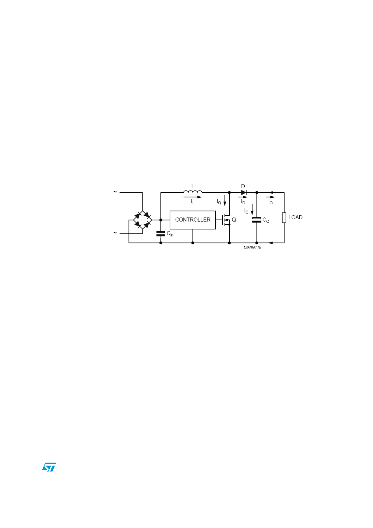
2 TM PFC operation (boost topology)
The operation of the PFC transition mode controlled boost converter, can be summarized in
the following description.
The AC mains voltage is rectified by a bridge and the rectified voltage is delivered to the
boost converter. This, using a switching technique, boosts the rectified input voltage to a
regulated DC output voltage (Vo).
The boost converter consists of a boost inductor (L), a controlled power switch (Q), a catch
diode (D), an output capacitor (Co) and, obviously, a control circuitry (see Figure 2).
The goal is to shape the input current in a sinusoidal fashion, in phase with the input
sinusoidal voltage. To do this the L6562A uses the transition mode technique.
Figure 2. Boost converter circuit
The error amplifier compares a partition of the output voltage of the boost converter with an
internal reference, generating an error signal proportional to the difference between them. If
the bandwidth of the error amplifier is narrow enough (below 20 Hz), the error signal is a DC
value over a given half-cycle.
The error signal is fed into the multiplier block and multiplied by a partition of the rectified
mains voltage. The result is a rectified sinusoid whose peak amplitude depends on the
mains peak voltage and the value of the error signal.
The output of the multiplier is in turn fed into the (+) input of the current comparator, thus it
represents a sinusoidal reference for PWM. In fact, as the voltage on the current sense pin
(instantaneous inductor current times the sense resistor) equals the value on the (+) of the
current comparator, the conduction of the MOSFET is terminated. As a consequence, the
peak inductor current is enveloped by a rectified sinusoid. As demonstrated in Section 3.3.4,
TM control causes a constant ON-time operation over each line half-cycle.
After the MOSFET has been turned off, the boost inductor discharges its energy into the
load until its current goes to zero. The boost inductor has now run out of energy, the drain
node is floating and the inductor resonates with the total capacitance of the drain. The drain
voltage drops rapidly below the instantaneous line voltage and the signal on ZCD drives the
MOSFET on again and another conversion cycle starts.
This low voltage across the MOSFET at turn-on reduces both the switching losses and the
total drain capacitance energy that is dissipated inside the MOSFET.
The resulting inductor current and the timing intervals of the MOSFET are shown in
Figure 3, where it is also shown that, by geometric relationships, the average input current
Doc ID 14690 Rev 2 5/36
Page 6
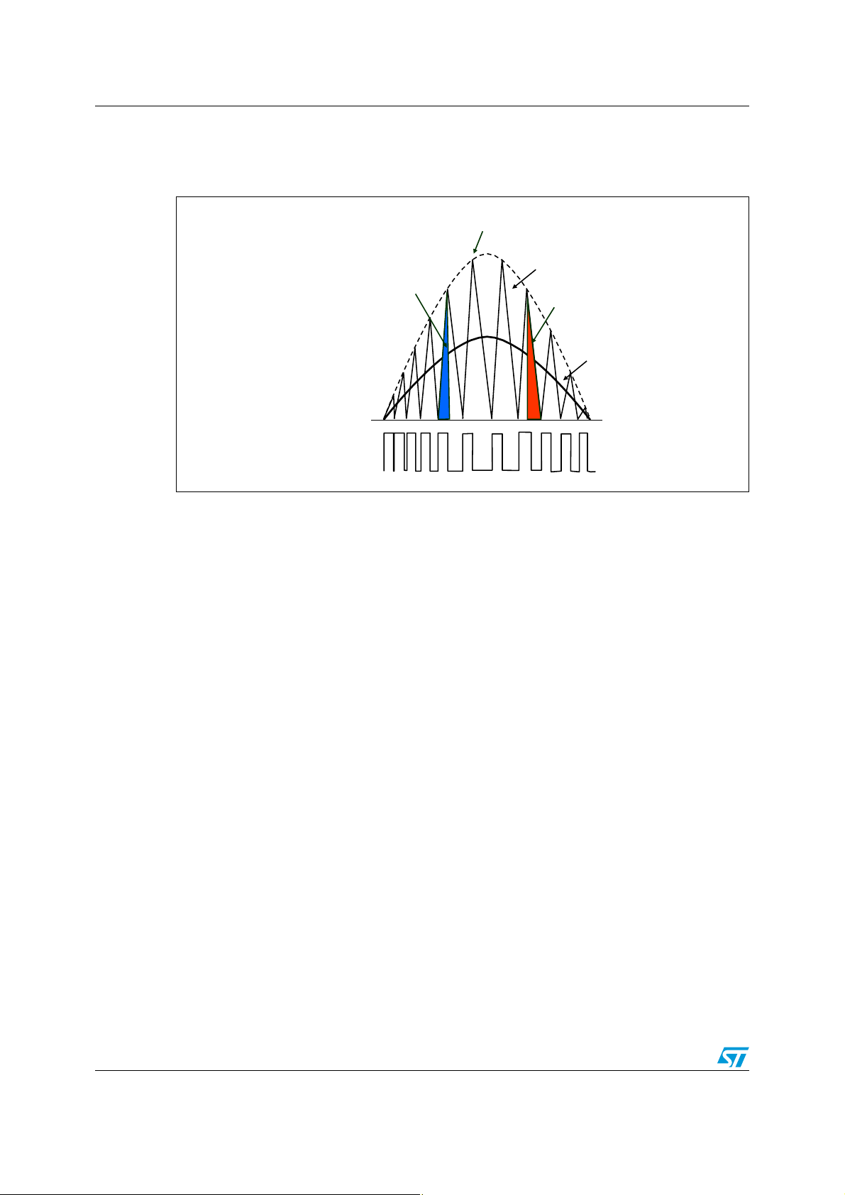
TM PFC operation (boost topology) AN2761
(the one which is drawn from the mains) is just one-half of the peak inductor current
waveform.
Figure 3. Inductor current waveform and MOSFET timing
ILpk
IL
ISW
ID
IAC
ON
MOSFET
OFF
The system operates not exactly on, but very close to, the boundary between continuous
and discontinuous current mode and that is why this system is called a transition mode PFC.
Besides the simplicity and the few external parts required, this system minimizes the
inductor size due to the low inductance value needed. On the other hand, the high current
ripple on the inductor involves high RMS current and high noise on the rectified main bus,
which needs a heavier EMI filter to be rejected. These drawbacks limit the use of the TM
PFC to lower power range applications.
6/36 Doc ID 14690 Rev 2
Page 7

AN2761 Designing a TM PFC
=
=
=
=
=
=
3 Designing a TM PFC
3.1 Input specification
The following is a possible design flowchart in reference to a transition mode PFC, using the
L6562A. This first part is a detailed specification of the operating conditions of the circuit that
is needed for the following calculation. In this example a 80 W, wide input range mains PFC
circuit has been considered. Some design criteria are also given.
● Mains voltage range (Vac rms):
● Minimum mains frequency:
● Rated output power (W):
min
max
l
out
Vac85VAC
(1)
Vac265VAC
Hz47f
W80P
(2)
(3)
Because the PFC is a boost topology the regulated output voltage depends strongly on the
maximum AC input voltage. In fact, for boost correct operation the output voltage must
always be higher than the input and thus, because the Vin max is V
VAC
max
2 374=⋅
pk
the output has been set at 400 Vdc as the typical value. If the input voltage is higher, as
typical in ballast applications, the output voltage must be set higher accordingly. As a rule of
thumb the output voltage must be set 6/7% higher than the maximum input voltage peak.
● Regulated DC output voltage (Vdc):
out
V400V
(4)
,
The target efficiency and PF are set here at minimum input voltage and maximum load.
They are used for the following operating condition calculations of the PFC. Of course at
high input voltage the efficiency is higher.
● Expected efficiency (%):
● Expected power factor:
Doc ID 14690 Rev 2 7/36
P
out
P
in
%93
==η
99.0PF
(5)
(6)
Page 8

Designing a TM PFC AN2761
=
Δ
=
Δ
=
=
=
=
Because of the narrow loop voltage bandwidth, the PFC output can face overvoltages at
startup or in case of load transients. To prevent from excessive output voltage that can
overstress the output components and the load, the L6562A integrates an OVP. The
overvoltage protection sets the extra voltage overimposed at Vout:
● Maximum output overvoltage (Vdc):
The mains frequency generates a 2f
L
V55OVP
(7)
voltage ripple on the output voltage at full load. The
ripple amplitude determines the current flowing into the output capacitor and the ESR.
Additionally, a certain holdup capability in case of mains dips can be requested of the PFC
in which case the output capacitor must also be dimensioned, taking into account the
required minimum voltage value (V
● Maximum output low-frequency ripple:
● Minimum output voltage after line drop
(Vdc):
● Holdup capability (ms):
) after the elapsed holdup time (t
out min
out
minout
Hold
),
Hold
V20V
V300V
ms10t
(8)
(9)
(10)
The PFC minimum switching frequency is one of the main parameters used to dimension
the boost inductor. Here we consider the switching frequency at low mains on the top of the
sinusoid and at full load conditions. As a rule of thumb, the switching frequency must be
higher than the audio bandwidth in order to avoid audible noise and additionally it must not
interfere with the L6562A minimum internal starter period, as given in the datasheet. On the
other hand, if the minimum frequency is set too high, the circuit shows excessive losses at a
higher input voltage and probably operates skipping switching cycles not only at light load.
The typical minimum frequency range is 20÷50 kHz for wide range operation.
● Minimum switching frequency (kHz):
minsw
kHz35f
(11)
In order to properly select the power components of the PFC and dimension the heat sinks
in case they are needed, the maximum operating ambient temperature around the PFC
circuitry must be known. Please note that this is not the maximum external operating
temperature of the entire equipment, but it is the local temperature at which the PFC
components are working.
● Maximum ambient temperature (°C):
8/36 Doc ID 14690 Rev 2
ambx
C50T
°
(12)
Page 9

AN2761 Designing a TM PFC
3.2 Operating condition
The first step is to define the main parameters of the circuit, using the specifications given in
Section 3.1:
● Rated DC output
current:
● Maximum input power:
● RMS input current:
● Peak inductor current:
As shown in
Figure 3, the inductor current is a triangle shape at switching frequency, and
P
in
I
=
in
I =
out
P
=
P
in
min
out
η
P
out
I
V
out
PFVAC
⋅
I22IL ⋅⋅=
inpk
out
P
in
I
=
in
pk
93
W80
V400
W80
A2.0
==
=⋅=
W86
⋅
W02.86100
=
99.0Vac85
=⋅⋅=
(13)
(14)
(15)
A02.1
(16)
A89.2A02.122IL
the peak of triangle is twice its average value. The average value of the inductor current is
exactly the peak of the input sine wave current, and therefore it can be easily calculated as
its rms value is obtained from equation
(15). To write down a complete inductor specification
for the inductor manufacturer we also provide the RMS and the AC current that can be
calculated using equations
(17) and (18).
● RMS inductor current:
● AC inductor
current:
IL ⋅=
2
rmsac
2
I
IL
inrms
3
2
IILIL −=
in
()( )
ac
rms
2
A18.1A02.1
=⋅=
(17)
3
22
=−=
(18)
A59.0A02.118.1IL
The current flowing in the inductor can be split in two parts, depending on the instant of
conduction. During the on time, the current increases from zero up to the peak value and
circulates into the switch, while during the following off-time the current decreases from
peak down to zero and circulates into the diode. Therefore there is a current with a triangular
wave, with the same peak value equal to the inductor current flowing into these two
components. Thus, it is also possible to calculate the RMS current flowing into the switch
and into the diode (
Figure 3), needed to calculate the losses of these two elements.
Doc ID 14690 Rev 2 9/36
Page 10

Designing a TM PFC AN2761
● RMS switch current:
● RMS diode current:
3.3 Power section design
3.3.1 Bridge rectifier
The input rectifier bridge can use standard, slow-recovery, low-cost devices. Typically a
600 V device is selected in order to have good margin against mains surges. An NTC
resistor limiting the current at plug-in is required to avoid overstress to the rectifier bridge
and fuse.
ILISW ⋅
pkrms
rms
ILID ⋅
pkrms
rms
VAC
1
6
24
⋅
−⋅=
9
π
min
V
out
(19)
Vac85
−⋅=
π
VAC
24
24
⋅
9
π
min
V
out
Vac85
V400
=⋅
V400
A01.1
=⋅
(20)
A59.0
1
A89.2ISW
6
24
⋅
⋅=
9
π
⋅
A89.2ID
⋅=
9
The rectifier bridge power dissipation can be calculated using equations
(21), (22), (23). The
threshold voltage and dynamic resistance of a single diode of the bridge can be found in the
component datasheet.
I2
⋅
I
inrms
I
avg_in
in
=
=
=
2
⋅
I2
in
=
π
A02.12
⋅
2
⋅
A02.12
π
A72.0
=
A46.0
=
(21)
(22)
The power dissipated on the bridge is:
bridge
2
diodebridge
inrms
2
IV4IR4P ⋅⋅+⋅⋅=
avg_inth
W98.1A46.0V14)A72.0(07.04P
=⋅⋅+⋅Ω⋅=
(23)
10/36 Doc ID 14690 Rev 2
Page 11

AN2761 Designing a TM PFC
=
3.3.2 Input capacitor
The input high-frequency filter capacitor (Cin) has to attenuate the switching noise due to
the high-frequency inductor current ripple (twice the average line current,
The worst conditions occur at the peak of the minimum rated input voltage.
The maximum high-frequency voltage ripple across Cin is usually imposed between 5% and
20% of the minimum rated input voltage. This is expressed by a coefficient r (from 0.05 to
0.2) as an input design parameter:
● Ripple voltage coefficient (%):
C
=
in
I
in
VACrf2
⋅⋅⋅π
minminsw
C
=
in
A02.1
Vac852.0kHz352
⋅⋅⋅π
In real conditions the input capacitance is designed taking the EMI filter into account and a
tolerance on the component of about 5% -10% (typical for polyester capacitors).
A commercial value of Cin = 0.22 µF has been selected. Of course a bigger capacitor
provides a benefit from the EMI point of view but worsens the THD, especially at high mains.
Therefore a compromise must be found between these two parameters. A good quality film
capacitor for this component must be selected in order to provide good filtering
effectiveness.
Figure 3).
2.0r
F26.0
μ=
(24)
(25)
3.3.3 Output capacitor
The output bulk capacitor (Co) selection depends on the DC output voltage (4), the allowed
overvoltage
The 100/120 Hz (twice the mains frequency) voltage ripple (
value) is a function of the capacitor impedance and the peak capacitor current:
With a low ESR capacitor the capacitive reactance is dominant, therefore:
C
O
ΔVout is usually selected in the range of 1.5% of the output voltage.
Although ESR usually does not affect the output ripple, it should be taken into account for
power loss calculations. The total RMS capacitor ripple current, including mains frequency
and switching frequency components, is:
(7) and the converter output power(3).
I
Crms
out
Vf2
Δ⋅⋅π
outl
≥
ΔVout = peak-to-peak ripple
I2V +
⋅⋅=Δ
outout
P
=
2
rms
out
VVf2
Δ⋅⋅⋅π
2
IIDI −=
out
Crms
1
2
)Cf22(
⋅⋅π
Ol
C
≥
outoutl
O
()()
ESR
2
W80
V20V400Hz472
⋅⋅⋅π
22
A56.0A20.0A59.0I
=−=
(26)
F8.33
μ=
(27)
(28)
Doc ID 14690 Rev 2 11/36
Page 12

Designing a TM PFC AN2761
(
()(
[
]
If the PFC stage has to guarantee a specified holdup time, the selection criterion of the
capacitance changes. C
has to deliver the output power for a certain time (t
O
Hold
) with a
specified maximum dropout voltage (Vout min) which is the minimum output voltage value
(which takes load regulation and output ripple into account). Vout min is the minimum output
operating voltage before the 'power fail' detection and consequent stopping by the
downstream system supplied by the PFC.
tP2
⋅⋅
out
Holdout
2
2
VVV
−Δ−
minout
C
=
O
C
=
O
()
out
()()
ms10W802
⋅⋅
22
V300V20V400
−−
F4.29
μ=
(29)
A 20% tolerance on the electrolytic capacitors has to be taken into account for the right
dimensioning.
Following the relationship
selected. The actual output voltage ripple with this capacitor is also calculated. In detail:
Holdup capability:
As expected the ripple variation on the output is:
V
out
3.3.4 Boost inductor
The boost inductor determines the working frequency of the converter. It is usually
calculated so that the minimum switching frequency is greater than the maximum frequency
of the L6562A internal starter (190 µs), to ensure a correct TM operation. Assuming unity
PF, it is possible to write:
(27) for this application, a capacitor Co = 47 µF (450 V) has been
⎡
O
out
⎢
t
hold
t
=
hold
I
out
=Δ
Cf2
⋅⋅π⋅
Ol
⎣
=
⋅
V
=Δ
out
2
)
−Δ−⋅
out
P2
⋅
out
−−⋅μ
W802
A20.0
F47Hz472
μ⋅⋅π⋅
⎤
2
VVVC
minout
⎥
⎦
(30)
22
)
V300V20V400F47
=
=
V41.14
ms43.17
(31)
ILL
⋅
=
pkpk
VAC2
⋅
(32)
In equation
)sin(ILL
),VAC(t
on
=ϑ
ϑ⋅⋅
)sin(VAC2
ϑ⋅⋅
(32) it is demonstrated that the ON-time doesn't depend on the mains phase
angle but it is constant over the entire mains cycle.
)sin(ILL
),VAC(t
off
12/36 Doc ID 14690 Rev 2
=ϑ
out
pk
ϑ⋅⋅
)sin(VAC2V
ϑ⋅⋅−
(33)
Page 13

AN2761 Designing a TM PFC
(
)
Ton and T
are respectively the ON-time and the OFF-time of the power MOSFET, ILpk is
off
the maximum peak inductor current in a line cycle, and θ is the instantaneous line phase in
the interval [0,Π]. Note that the ON-time is constant over a line cycle.
As previously stated, IL
is twice the line-frequency peak current (16), which is related to
pk
the input power and the input mains voltage. Substituting this relationship in the expressions
of T
and T
on
, after some algebra it is possible to find the instantaneous switching
off
frequency along a line cycle:
sw
),VAC(f
1
=θ
TT
+
1
=
PL2
⋅⋅
inoffon
2
⋅
out
V
out
)sin(VAC2VVAC
θ⋅⋅−⋅
(34)
The switching frequency is the minimum at the top of the sinusoid (θ = Π /2 rad =>
sin θ =1), maximum at the zero-crossings of the line voltage (θ = 0 rad or Π rad=> sin θ =0),
where T
The absolute minimum frequency f
minimum mains voltage VAC
=0 µs.
off
can occur at either the maximum VAC
swmin
, thus the inductor value is defined by the formula:
min
2
)VAC(L
=
out
⋅⋅⋅
)VAC2V(VAC
⋅−⋅
VPf2
outinminsw
max
or the
(35)
After calculating the values of the inductor at low mains and at high mains L(VAC
L(VAC
) (35), the minimum value has to be taken into account. It becomes the maximum
min
inductance value for the PFC dimensioning.
()
)VAC(L
=
min
()
)VAC(L
=
max
2
⋅−⋅
⋅⋅⋅
2
⋅−⋅
⋅⋅⋅
)Vac852V400(Vac85
V400W02.86kHz352
V400W02.86kHz352
mH73.0
=
)Vac2652V400(Vac265
mH83.0
=
For this application a 0.7 mH boost inductance has been selected.
max
),
(36)
(37)
Doc ID 14690 Rev 2 13/36
Page 14

Designing a TM PFC AN2761
,
Figure 4. Switching frequency fixing the line voltage
Frequency modulation with the Line half-period
1000
VACmax
100
Figure 4
kHz
10
shows the switching frequency versus the θ angle calculated with the (35), a 0.7
VACmin
1
0.0 0.5 1.0 1.5 2.0 2.5 3.0
θ
line half-period
⎝,
⎝
mH boost inductance and fixing the line voltage at minimum and maximum values.
The minimum switching frequency can be recalculated for the selected inductance value
inverting equation
From the comparison of the f
(35) as follows:
minsw
swmin
)VAC(f
=
(VAC
min
2
out
VPL2
⋅⋅⋅
outin
), f
swmin
(VAC
)VAC2V(VAC
⋅−⋅
) with L = 0.7 mH the actual,
max
(38)
calculated minimum switching frequency is 37 kHz, as expected.
The core size is determined assuming a peak flux density Bx ≅ 0.25T (depending on ferrite
grade selected and relevant specific losses) and calculating the maximum current according
to
(58), as a function of the maximum current sense pin clamping voltage and sense resistor
value.
DC and AC copper losses and ferrite losses must also be calculated to determine the
maximum temperature rise of the inductor.
3.3.5 Power MOSFET selection and dissipation
The selection of the MOSFET concerns mainly its R
power
voltage admitted
480 V) is selected. Using its current rating as a rule of thumb, we can select a device having
~ 3 times the RMS switch current (19) but the power dissipation calculation gives the final
confirmation that the selected device is the right one for the circuit also taking into account
the heat sink dimensions. In this 80W TM PFC application an STP8NM50 MOSFET has
been selected.
The MOSFET' s power dissipation depends on conduction, switching and capacitive losses.
14/36 Doc ID 14690 Rev 2
(3), since the breakdown voltage is fixed just by the output voltage (4), plus the over-
(7) and a safety margin (20%). Thus, a voltage rating of 500 V (1.2 · Vout =
, which depends on the output
DS(on)
Page 15

AN2761 Designing a TM PFC
(
⋅⋅⋅
=
The conduction losses at maximum load and minimum input voltage are calculated by:
Because normally in the datasheets R
rmsoncond
is given at ambient temperature (25°C) to
DS(on)
2
)
)VAC(ISWRDS)VAC(P ⋅=
(39)
calculate correctly the conduction losses at 100 °C (typical MOSFET junction operating
temperature) a factor of 1.75 to 2 should be taken into account. The exact factor can be
found in the device datasheet.
Now, the conduction losses normalized to 1Ω R
of P
and VAC can be calculated, combining equations (39) and (19):
in
⎛
⎜
′
rmscond
2
2))VAC(ISW(2)VAC(P
⋅=⋅=
⎜
⎝
at ambient temperature as a function
DS(on)
2
P
in
PFVAC2
⋅⋅
16
2
⋅
−⋅
π
3
V
⎞
VAC2
⋅
⎟
⎟
out
⎠
(40)
The switching losses in the MOSFET occur only at turnoff because of the TM operation and
can be basically expressed by:
swfallMOSMOSswitch
)VAC(ftIV)VAC(P
(41)
(41) represents the crossing between the MOSFET current that decreases linearly during
the fall time and the voltage on the MOSFET drain that increases. In fact during the fall time
the current of the boost inductor flows into the parasitic capacitance of the MOSFET
charging it. For this reason switching losses depend also on the total drain capacitance.
Because switching frequency depends on the input line voltage and the phase angle on the
sinusoidal waveform, it can be demonstrated that from
(41) the switching losses per 1 µs of
current fall time and 1 nF of total drain capacitance can be written as:
The value t
′
at turn-off can be found in the MOSFET datasheet.
fall
VIL)VAC(P
π
1
⋅⋅=
outpkswitch
∫
π
0
2
()
sw
ϑ⋅θ⋅ϑ
d),VAC(fsin
(42)
At turn-on the losses are due to the discharge of the total drain capacitance inside the
MOSFET itself.
In general, the capacitive losses are given by:
1
)VAC(P
2
where C
is the total drain capacitance including the MOSFET and the other parasitic
d
capacitances such as the inductor at the drain node, and V
2
⋅⋅⋅=
MOS
dcap
sw
)VAC(fVC
is the drain voltage at
MOS
(43)
MOSFET turn-on.
Doc ID 14690 Rev 2 15/36
Page 16

Designing a TM PFC AN2761
ϑ−π=ϑ
ϑ
ϑ
ϑ
ϑ
Taking into account the frequency variation with the input line voltage and the phase angle
similar to
(43), a detailed description of the capacitive losses per 1 nF of total drain
capacitance can be calculated as:
′
θ1
and θ2 depend on input voltage and they are defined as follows:
)VAC(P
ϑ
2
121
()
⋅=
∫
π
ϑ
1
=ϑ
arcsin
1
Figure 5. Transition angle versus input
1.0
1.0
0.9
0.9
0.8
0.8
0.7
0.7
0.6
0.6
0.5
0.5
0.4
0.4
0.3
0.3
0.2
0.2
0.1
0.1
0.0
0.0
0.00 0.50 1.00 1.50 2.00 2.50 3.00
0.00 0.50 1.00 1.50 2.00 2.50 3.00
voltage
1
1
V
V
22
22
angle
angle
out
out
VAC
VAC
)sin(
)sin(
ϑπϑ
=
ϑπϑ
=
12
12
2
sw
outcap
⎛
⎜
⎜
⎝
⎞
V
out
⎟
⎟
VAC22
⎠
12
ϑ⋅ϑ−
d),VAC(fVVAC22
Figure 6. Capacitive losses
VDRAIN
VDRAIN
Vin1
Vin1
Vin2
Vin2
ZVS
ZVS
Pcap
Pcap
(44)
(45)
(46)
t
t
The dependence on the input voltage is shown in
Figure 5 and 6. On the right is represented
the drain voltage waveform. The MOSFET turn-on occurs just on the valley because the
inductor has depleted its energy and therefore it can resonate with the drain capacitance.
The details are in the following ZCD pin description. It is clear that for an input voltage
theoretically lower than half of the output voltage the resonance ideally should reach zero
achieving zero-voltage operation, therefore there are no losses relevant to this edge. For
input voltage corresponding to a positive value of the valley, capacitive losses are not
generated. However, the MOSFET turn-on always occurs at the minimum voltage of the
resonance and therefore the losses are minimized.
In practice it is possible to estimate the total switching and capacitive losses by solving the
integral of the switching frequency depending on sin(θ) on the half-line cycle.
16/36 Doc ID 14690 Rev 2
Page 17

AN2761 Designing a TM PFC
The total loss function of the input mains voltage is the sum of the three previous losses, see
equations
(40), (42) and (44) multiplied for the MOSFET parameters:
′
⋅=
condonloss
2
t
fall
)VAC(PRDS)VAC(P
′
⋅+
C
d
′
⋅+
capdsw
)VAC(PC)VAC(P
(47)
Figure 7 shows the trend of the total losses (47) on the line voltage for the selected
MOSFET STP8NM50. Capacitive losses are dominant at high mains voltage and the major
contribution came from the conduction losses at low and medium mains voltage.
Figure 7. Conduction losses and total losses in the STP8NM50 MOSFET for the
80W TM PFC
MOSFET Total losses
1.8
1.6
1.4
1.2
1.0
W
0.8
0.6
0.4
0.2
0.0
85 130 175 220 265
Vin_ac [Vrms]
Pcond(Vi)*Ron
Ploss(Vi)
From (47) using the data relevant to the MOSFET selected, and calculating the losses at
VAC
and VAC
min
, we observe that the maximum total losses occurs at VAC
max
1.69 W. From this number and the maximum ambient temperature
thermal resistance required to keep the junction temperature below 125 °C is:
=
R
th
If the result of equation
−°
loss
(48) is lower than the junction-ambient thermal resistance given in
the MOSFET datasheet for the selected device package, a heat sink must be used.
3.3.6 Boost diode selection
Following a similar criterion as that for the MOSFET, the output rectifier can also be
selected. A minimum breakdown voltage of 1.2·(Vout + ΔVovp) and a current rating higher
than 3·Iout
is then confirmed by the thermal calculation. If the diode junction temperature operates
(13) can be chosen for a rough initial selection of the rectifier. The correct choice
which is
min
(12), the total maximum
°−°
TC125
ambx
)VAC(P
Doc ID 14690 Rev 2 17/36
=
R
th
C50C125
=
W69.1
°
C
50.44
W
(48)
Page 18

Designing a TM PFC AN2761
(
V
within 125 °C the device has been selected correctly, otherwise a bigger device must be
selected.
In this 80 W application an STTH1L06 (600 V, 1 A) has been selected.
The rectifier AVG
threshold voltage) and R
(13) and RMS (20) current values and the parameter V
(dynamic resistance) given in the datasheet allow calculating the
d
rectifier losses.
From the STTH1L06 datasheet, V
From
(12) and (49) the maximum thermal resistance to keep the junction temperature below
2
IDRIVP ⋅+⋅=
doutthdiode
th
rms
125 °C is then:
TC125R−°
=
th
Because the calculated R
th
ambx
P
diode
is higher than the STTH1L06 thermal resistance junction-
ambient, no any heat sink is needed for the rectifier.
3.4 L6562A biasing circuitry
Following the dimensioning of the power components, the biasing circuitry for the L6562A is
also described. For reference, the internal schematic of the L6562A is represented below in
Figure 8.
is 0.89 V and Rd is 0.165 Ω.
diode
C50C125
R
=
th
°−°
317
=
W23.0
°
W
(rectifier
th
2
)
=⋅Ω+⋅=
C
(49)
W23.0A59.0165.0A2.0V89.0P
(50)
For more details on the internal function, please refer to the datasheet.
Figure 8. L6562A internal schematic
INV COMP MULT CS
123 4
ERROR
INTERNAL
SUPPLY BUS
UVLO
V
REF2
AM PLIFIER
VREF
-
+
1.4 V
0.7 V
5
= 2.5V
ZCD
-
+
OVERVOLTAGE
DETECTION
DYN
OVP
DIS
ZERO CURRENT
+
-
STAT
OVP
DETECTO R
MULTIPLI ER AND
THD OPTIMIZER
1 V
+-
COMPARATOR
R
Q
S
PWM
STARTER
Starter
stop
LEADING-EDGE
BLANKING
DRIVER
& CLAMP
DIS
-
0.45 V
+
0.2 V
VOLTAGE
REGULA TOR
8
CC
25 V
LOWER & UP PER
CLAMPS
VCC
7
GD
6
GND
18/36 Doc ID 14690 Rev 2
Page 19

AN2761 Designing a TM PFC
● Pin 1 (INV): This pin is connected both to the inverting input of the E/A and to the DIS
circuitry. A resistive divider is connected between the boost regulated output voltage
and this pin. The internal reference on the non-inverting input of the E/A is 2.5 V (typ),
while the DIS intervention threshold is 27 µA (typ). R
outH
and R
are then selected as
outL
follows:
V
Δ
R
outH
R
outH
R
outL
R
outL
OVP
=
μ
V
out
R
outH
= Ω=
159
R
A27
V5.2
outH
R
outH
1
−= 1591
R
outL
R
outL
V55
= M03.2
μ
A27
V400
V5.2
M2
Ω
= k6.12
159
Ω=
=−=
(51)
(52)
(53)
The commercial values selected are R
Please note that for R
a resistor with a suitable voltage rating (>400 V) is needed, or
outH
= 2 MΩ and R
outH
= 15 kΩ in parallel to a 82 kΩ.
outL
more resistors in series have to be used.
This pin can also be used as an ON/OFF control input if tied to GND by an open collector or
open drain.
● Pin 2 (COMP): This pin is the output of the E/A that is fed to one of the two inputs of the
multiplier. A feedback compensation network is placed between this pin and INV (1). It
has to be designed with a narrow bandwidth in order to avoid that the system rejects
the output voltage ripple (100 Hz) that would bring high distortion of the input current
waveform. A simple criterion to define the capacitance value is to set the bandwidth
(BW) from 20 to 30 Hz. The compensation network can be just a capacitor, providing a
low-frequency pole as well as a high DC gain. A more complex network, typically a
type-II CRC network providing 2 poles and a zero, is more suitable for constant power
loads like a downstream converter.
In case a single capacitor is used, it can be dimensioned using the following formulas:
BW
=
()
C
=
onCompensati
1
CR//R2
⋅⋅π
onCompensatioutLoutH
1
()
BWR//R2
⋅⋅π
outLoutH
(54)
(55)
Doc ID 14690 Rev 2 19/36
Page 20

Designing a TM PFC AN2761
μ=Ω
=
For a more complex compensation network calculation please refer to [2], [3].
For this 80 W TM PFC, a CRC network providing two poles and a zero has been
implemented, using the following values:
compP
nF150C
= F2.2C
compS
compS
k22R
(56)
to which corresponds the following open-loop transfer function and its phase function.
Figure 9. Bode plot - open-loop transfer
100
0
dB
-100
-200
0.1 1 10 100 1000
function
Open Loop Transfer Funct i on
IFI
f [Hz]
The two Bode plot charts are in reference to the PFC operating at 265Vac and full load
Figure 9 and 10). In this condition the crossover frequency is fc = 28 Hz, the phase margin
(
is 55°. The third harmonic distortion introduced by the E/A 100 Hz residual ripple is below
3%.
● Pin 4 (CS): The pin #4 is the inverting input of the current sense comparator. Through
this pin, the L6562A senses the instantaneous inductor current, converted to a
proportional voltage by an external sense resistor (R
threshold set by the multiplier output, the PWM latch is reset and the power MOSFET is
turned off. The MOSFET stays in OFF-state until the PWM latch is reset by the ZCD
signal. The pin is equipped with 200 ns leading-edge blanking to improve noise
immunity.
Figure 10. Bode plot - phase
Phase F
-100
deg
-150
-200
0.1 1 10 100 1000
f [Hz]
). As this signal crosses the
s
The sense resistor value (R
) can be calculated as follows. For the 80 W PFC it is:
s
R <
s
Vcs
IL
min
R
pk
s
V0.1
A89.2
Ω=< 34.0
(57)
where:
–IL
–Vcs
is the maximum peak current in the inductor, calculated as described in (16)
pk
= 1.0 V is the minimum voltage allowed on the L6562A current sense (in
min
the datasheet)
20/36 Doc ID 14690 Rev 2
Page 21

AN2761 Designing a TM PFC
(
⋅−⋅
=
Because the internal current sense clamping sets the maximum current that can flow in the
inductor, the maximum peak of the inductor current is calculated considering the maximum
voltage Vcs
allowed on the L6562A (in the datasheet):
max
Vcs
IL =
pkx
max
R
s
IL
pkx
=
V16.1
34.0
Ω
A41.3
=
(58)
The calculated IL
is the limit at which the boost inductor saturates and it is used for
pkx
calculating the inductor number of turns and air gap length.
The power dissipated in R
is given by:
s
2
ISWRP ⋅=
rmsss
2
s
)
W35.0A01.134.0P
=⋅Ω=
(59)
According to the result two parallel resistors of 0.68 Ω with 0.25 W of power rating have
been selected.
● Pin 3 (MULT): The MULT pin is the second multiplier input. It is connected, through a
resistive divider, to the rectified mains to get a sinusoidal voltage reference. The
multiplier can be described by the relationship:
V)V5.2V(kV
MULTCOMPCS
(60)
where:
–V
(multiplier output) is the reference for the current sense
CS
– k = 0.38 (typ) is the multiplier gain
–V
–V
is the voltage on pin 2 (E/A output)
COMP
is the voltage on pin 3
MULT
Doc ID 14690 Rev 2 21/36
Page 22

Designing a TM PFC AN2761
Figure 11. Multiplier characteristics family
Multiplier characteristic
1.2
Upper Volt. Clamp
1.1
1.0
0.9
0.8
0.7
0.6
0.5
Vcs (pi n 4) (V )
0.4
0.3
0.2
0.1
0.0
-0.1
0.00.20.40.60.81.01.21.41.61.82.02.22.42.62.83.0
5.75 V
5 V
4.5V
VMULT (p in3) (V)
V COMP (pin2) (V
4 V
)
3.5V
3 V
2.5 V
A complete description is given in Figure 11, which shows the typical multiplier
characteristics family. The linear operation of the multiplier is guaranteed within the range 0
to 3 V of V
and the range 0 to 1.16 V (typ) of Vcs, while the minimum guaranteed value
MULT
of the maximum slope of the characteristics family (typ) is:
dV
dV
CS
MULT
V
1.1
=
V
(61)
Taking this into account, the following is the suggested procedure to properly set the
operating point of the multiplier.
First, the maximum peak value for V
MULT
, V
MULTmax
is selected. This value, which occurs at
maximum mains voltage, should be 3 V or nearly so in wide-range mains and less in case of
single mains. The sense resistor selected is R
= 0.34 Ω and it is described in the paragraph
s
concerning pin 4 of this section. The maximum peak value, occurring at maximum mains
voltage is:
VMULT ⋅
where IL
=
max
and Rs have been already calculated, and 1.1 V/V is the multiplier maximum
pk
RIL
⋅
VAC
spk
1.1
VAC
max
min
VMULT
max
=
34.0A89.2
Ω⋅
1.1
Vac265
=⋅
Vac85
(62)
V06.3
slope reported in the datasheet.
(62) the maximum required divider ratio is calculated as:
From
V
k
=
p
maxMULT
max
=
⋅
VAC2
⋅
22/36 Doc ID 14690 Rev 2
V06.3
3
−
1016.8
⋅=
(63)
Vac2652
Page 23

AN2761 Designing a TM PFC
Supposing a 200 µA current flowing into the multiplier divider, the lower resistor value can
be calculated:
−
=
R
multH
k
In this application example R
note that for R
a resistor with a suitable voltage rating (>400 V) is needed, or more
multH
k1
p
R
multL
p
= 2 MΩ and R
multH
=
3
−
⋅−
1016.81
−
3
⋅
1016.8
= 15 kΩ have been selected. Please
multL
Ω=Ω
M85.1k15
(64)
resistors in series must be used.
The voltage on the multiplier pin with the selected component values recalculated is 0.89 V
at minimum line voltage and is 2.8 V at maximum line voltage. The multiplier works correctly
within its linear region.
● Pin 5 (ZCD): Pin #5 is the input of the zero current detector circuit. In transition mode
PFC, the ZCD pin is connected, through a limiting resistor, to the auxiliary winding of
the boost inductor. The ZCD circuit is negative-going edge triggered. When the voltage
on the pin falls below 0.7 V, it sets the PWM latch and the MOSFET is turned on. To do
so the circuit must first be armed. Prior to falling below 0.7 V, the voltage on pin 5 must
experience a positive-going edge exceeding 1.4 V (due to the MOSFET's turnoff). The
maximum main-to-auxiliary winding turn ratio, nmax, has to ensure that the voltage
delivered to the pin during the MOSFET's OFF-time is sufficient to arm the ZCD circuit.
A safe margin of 15% is added.
n
maxn
primary
n
auxiliary
==
VAC2V
⋅−
maxout
15.1V4.1
⋅
maxn =
=
Vac2652V400
⋅−
15.1V4.1
⋅
(65)
7.15
If the winding is also used for supplying the IC, the above criterion may not be compatible
with the Vcc voltage range. To solve this incompatibility the self-supply network shown in the
schematic of
Figure 18 can be used.
The minimum value of the limiting resistor can be found considering the maximum voltage
across the auxiliary winding with a selected turn ratio = 10 and assuming 0.8 mA current
through the pin.
V
out
V
−
ZCDH
aux
max
mA8.0
V
−
ZCDL
R
1
R
mA8.0
= 0 V are the upper and lower ZCD clamp voltages of the L6562A.
V
ZCDH
R
R
=
2
= 5.7 V and V
=
1
⋅
n
ZCDL
n
VAC2
aux
Considering the higher value between the two calculated, R
V400
−
10
= k9.42
= k8.46
2
V7.5
mA8.0
⋅
Vac2652
−
10
V0
mA8.0
= 47 kΩ has been selected
ZCD
Ω=
(66)
(67)
Ω=
as the limiting resistor.
Doc ID 14690 Rev 2 23/36
Page 24

Designing a TM PFC AN2761
Figure 12. Optimum MOSFET turn-on
VDRAIN
VDRAIN
Vout
Vout
Vipk
Vipk
t
Vzcd
Vzcd
5.7
5.7
1.4
1.4
0.7
0.7
t
t
t
The actual value can then be tuned trying to make the turn-on of the MOSFET occur just on
the valley of the drain voltage (which is resonating because the boost inductor has run out of
energy, (
● Pin 6 (GND): This pin acts as the current return both for the signal internal circuitry and
Figure 12).This minimizes the power dissipation at turn-on.
for the gate drive current. When laying out the printed circuit board, these two paths
should run separately.
● Pin 7 (GD) is the output of the driver. The pin is able to drive an external MOSFET with
600 mA source and 800 mA sink capability. The high-level voltage of this pin is clamped
at about 12 V to avoid excessive gate voltages in case the pin is supplied with a high
Vcc. To avoid undesired switch-on of the external MOSFET because of some leakage
current when the supply of the L6562A is below the UVLO threshold, an internal pulldown circuit holds the pin low. The circuit guarantees 1.1 V maximum on the pin
(at I
= 2 mA), with Vcc > Vcc_ON. This allows omitting the "bleeder" resistor
sink
connected between the gate and the source of the external MOSFET used for this
purpose.
● Pin 8 (Vcc) is the supply of the device. This pin is externally connected to the startup
circuit (usually, one resistor connected to the rectified mains) and to the self-supply
circuit. Whatever the configuration of the self-supply system, a capacitor is connected
between this pin and ground. To start the L6562A, the voltage must exceed the startup
threshold (12.5 V typ). Below this value the device does not work and consumes less
than 30 µA (typ) from Vcc. This allows the use of high value startup resistors (in the
hundreds kΩ), which reduces power consumption and optimizes system efficiency at
low load, especially in wide-range mains applications. When operating, the current
consumption (of the device only, not considering the gate drive current) rises to a value
depending on the operating conditions but never exceeding 3.75 mA. The device keeps
on working as long as the supply voltage is over the UVLO threshold (10.5 V max). If
the Vcc voltage exceeds 25 V, an internal clamping circuitry, is activated in order to
clamp the voltage. Please remember that during normal operation the internal clamp
does not have to limit the voltage, in which case the power consumption of the device
increases considerably and its junction temperature also increases. The suggested
operating condition for safe operation of the device is powering the L6562A with a Vcc
below the minimum calmping voltage of pin 8.
24/36 Doc ID 14690 Rev 2
Page 25

AN2761 Design example using the L6562A-TM PFC Excel spreadsheet
4 Design example using the L6562A-TM PFC Excel
spreadsheet
An Excel spreadsheet has been developed to allow a quick and easy design of a boost PFC
preregulator using the STM L6562A controller, operating in transition mode.
Figure 13 shows the first sheet already precompiled with the input design data used in
Section 3: Designing a TM PFC.
Figure 13. Excel spreadsheet design specification input table
Parameter Name Value Unit [ ]
Mains Voltage Range VacMin 85 VACrms
Mains Voltage Range VacMax 265 VACrms
Min.Mains Frequency fl 47 Hz
Regulated Output Voltage Vout 400 Vdc
Rated Output Power Pout 80 W
Max. Output Low Frequency Ripple ǻ Vout
Max. Output Overvoltage ǻOVP 55 Vdc
Holdup Capability Thold
Min. Output Voltage after Line drop VoutMin 300 Vdc
Min. Switching Frequency: fmin 35 kHz
Expected Efficiency
Expected Power Factor PF 0.99 ---
Maximum Ambient Temperature Tambx 50 C
η
20
10
93 %
Vpk-pk
ms
Figure 14. Other design data
Parameter Name Value Unit [ ]
Maximum Magnetic Flux Density Bx 0.25 T
Ripple VoltageCoefficient r 0.2 ---
The tool is able to generate a complete part list of the PFC schematic represented in
Figure 15, including the power dissipation calculation of the main components.
Doc ID 14690 Rev 2 25/36
Page 26

Design example using the L6562A-TM PFC Excel spreadsheet AN2761
Figure 15. Excel spreadsheet TM PFC schematic
L
FUSE
FUSE
4A/250V
4A/250V
Vac
Vac
85V
85V
to
to
265V
265V
L
RcompS
RmultH
RmultH
+
+
Cin
-
-
Cin
RmultL
RmultL
Vcc
Vcc
VCC
VCC
MULT
MULT
Rzcd
Rzcd
8
8
3
3
ZCD
ZCD
COMP
COMP
5
5
L6562A
L6562A
GND CS
GND CS
CcompS
CcompS
CcompP
CcompP
2
2
6
6
RcompS
INV
INV
1
1
7
7
4
4
GD
GD
Rsense
Rsense
D
D
MOS
MOS
Rout
Rout
Rout
Rout
H
H
Cout
Cout
L
L
The bill of material in Figure 16 is automatically compiled by the Excel spreadsheet. It
summarizes all selected components and some salient data.
Figure 16. Excel spreadsheet BOM - 80 W TM PFC based on L6562A
80W TM PFC BASED ON L6562A
BILL OF MATERIAL
Selected
Value
Unit
[ ]
BRIDGE RECTIFIER W08
MOSFET P/N STP8NM50
DIODE P/N STTH1L06
Inductor Lx 0.70 mH
Max peak Inductor current Ilpkx 3.41 A
Sense resistor Rsx 0.34 ȍ
Power dissipation Ps 0.35 W
INPUT Capacitor Cin 0.22 µF
OUTPUT Capacitor Cout 47 µF
MULT Divider Rmult L 15 kȍ
Rmult H 2000 kȍ
ZCD Resistor Rzcd 47 kȍ
Feedback Divider RoutH 2000 kȍ
RoutL 12.68 kȍ
Comp Network CcompP 150 nF
CcompS 2200 nF
RcompS 22 kȍ
IC Controller L6562A
26/36 Doc ID 14690 Rev 2
Page 27

AN2761 EVL6562A-TM-80W demonstration board
5 EVL6562A-TM-80W demonstration board
Figure 17. EVL6562A-TM-80W demonstration board
Figure 18. Wide range 80W demonstration board electrical circuit (EVL6562A-TM-
80W)
Vo=400V
Vo=400V
Po=80W
Po=80W
R11
R11
Ω
Ω
1M
1M
R12
R12
1M
1M
Ω
Ω
C6
C6
47 µF
47 µF
450V
450V
R13B
R13B
82 k
82 k
Ω
Ω
Ω
Ω
C1
F1
F1
4A/250V
4A/250V
Vac
Vac
88V
88V
to
to
264V
264V
Figure 18
P1
P1
+
+
W08
W08
-
-
Boost Inductor Spec (ITACOIL E2543/E)
Boost Inductor Spec (ITACOIL E2543/E)
shows the schematic of an application board. It has been dimensioned using the
C1
0.22 µF
0.22 µF
630V
630V
R3
R3
15 k
15 k
Ω
Ω
E25x13x7 core, N67 ferrite
E25x13x7 core, N67 ferrite
1.5 mm gap for 0.7 mH primary inductance
1.5 mm gap for 0.7 mH primary inductance
Primary: 102 turns 20x0.1 mm
Primary: 102 turns 20x0.1 mm
Secondary: 10 turns 0.1 mm
Secondary: 10 turns 0.1 mm
Excel tool presented in
R4
R5
R4
R5
Ω
Ω
Ω
Ω
270 k
270 k
270 k
270 k
R1
R1
1 M
1 M
Ω
Ω
R2
R2
1 M
1 M
Ω
Ω
C2
C2
10nF
10nF
C29
C29
22 µF
22 µF
25V
25V
Section 4.
D8
D8
1N4148
1N4148
D2
D2
1N5248B
1N5248B
C5
C5
10 nF
10 nF
VCC
VCC
MULT
MULT
100 nF
100 nF
R14
R14
100
100
Ω
Ω
R6
R6
47 k
47 k
Ω
Ω
ZCD COMP INV
ZCD COMP INV
8
8
3
3
GND
GND
C4
C4
T1
T1
C3 - 2200 nF
C3 - 2200 nF
150 nF
150 nF
5
21
5
21
L6562A
L6562A
6
6
C23
C23
CS
CS
R50 - 22 kΩ
R50 - 22 kΩ
GD
GD
7
7
4
4
R15
R15
SHORTED
SHORTED
D1
D1
NTC
STP8NM50FP
STP8NM50FP
R10
R10
0.68 Ω
0.68 Ω
0.25W
0.25W
NTC
2.5
2.5
Ω
Ω
Q1
Q1
R13
R13
15 k
15 k
STTH1L06
STTH1L06
R7
R7
33
33
Ω
Ω
R8
R8
47k
47k
Ω
Ω
R9
R9
0.68 Ω
0.68 Ω
0.25W
0.25W
The board implements a power factor correction (PFC) preregulator delivering 80 W
continuous power, on a regulated 400 V rail from a wide-range mains voltage and providing
Doc ID 14690 Rev 2 27/36
Page 28

EVL6562A-TM-80W demonstration board AN2761
for the reduction of the mains harmonics, which complies with the European norm
EN61000-3-2 or the Japanese norm JEIDA-MITI. This rail is the input for the cascaded
isolated DC-DC converter provides the output rails required by the load. The board has
been designed to allow full-load operation in still air.
The power stage of the PFC is a conventional boost converter, connected to the output of
the rectifier bridge D2. It includes the coil T1, the diode D1 and the capacitor C6. The boost
switch is represented by the power MOSFET Q1. The NTC limits the inrush current at plugin. It has been connected on the DC rail, in series to the output electrolytic capacitor, in
order to improve the efficiency during low line operation because the rectifier RMS current is
significantly lower than the AC input current at minimum input voltage and maximum load.
Even in this position the NTC limits the surge current due to the output electrolytic capacitor
as well.
At startup the L6562A is powered by the Vcc capacitor C29 that is charged via the resistors
R4 and R5. Then the T1 secondary winding and the charge pump circuit (R14, C5, D2 and
D8) generate the Vcc voltage powering the L6562A during normal operations. The divider
composed of R1 + R2 and R3 provides the L6562A multiplier with the information of the
instantaneous voltage that is used to modulate the boost current. The divider composed of
R11 + R12 and R13A in parallel with R13B is dedicated to sense the output voltage.
The board is not equipped with an input EMI filter. The filter must be added in the final
application circuit by the user.
28/36 Doc ID 14690 Rev 2
Page 29

AN2761 Test results and significant waveforms
6 Test results and significant waveforms
One of the main purposes of a PFC preconditioner is the correction of input current
distortion, decreasing the harmonic contents below the limits of the relevant regulations.
Therefore, this demonstration board has been tested according to the European standard
EN61000-3-2 Class-D and Japanese standard JEIDA-MITI Class-D, at full load at both
nominal input voltage mains.
As shown in the following
Figure 19 and 20, the circuit is able to reduce the harmonics well
below the limits of both regulations from full load down to light load. Please note that all
measures and waveforms have been done using a Pi-filter for filtering the noise coming from
the circuit, using a 25 mH common mode choke and two 220NF-X2 filter capacitors.
Figure 19. EVL6562A-TM-80W compliance to
0.1
0.01
Harmonic current (A)
0.001
0.0001
EN61000-3-2 standard
Measurements @ 230Vac Full load EN61000-3-2 cl a ss D limits
1
1 3 5 7 9 111315171921232527293133353739
Harmonic Order (n)
Vin = 230 Vac - 50 Hz, Pout = 80 W
THD = 10.48 %, PF = 0.973
Figure 20. EVL6562A-TM-80W compliance to
JEIDA-MITI standard
Measurements @ 100Vac Full load JEIDA-MITI class D limits
1
0.1
0.01
Harmonic current (A)
0.001
0.0001
1 3 5 7 9 111315171921232527293133353739
Harmonic Order (n)
Vin = 100 Vac - 50 Hz, Pout = 80 W
THD = 3.18 %, PF = 0.997
Doc ID 14690 Rev 2 29/36
Page 30

Test results and significant waveforms AN2761
Figure 21. EVL6562A-TM-80W
1.000
0.975
0.950
0.925
0.900
PF
0.875
0.850
0.825
0.800
power factor vs. Vin and load
Pout = 80W
Pout = 40W
Pout = 20W
80 130 180 230 280
Vin (Vac)
The power factor (PF) and the total harmonic distortion (THD) have been measured and are
illustrated in
Figure 21 and 22. As shown, the PF measured at full load and half load
remains close to unity throughout the input voltage mains range while, when the circuit is
delivering 20 W, it decreases at high mains range. THD is low, remaining within 16% at
maximum input voltage.
Figure 22. EVL6562A-TM-80W
THD vs. Vin and load
20
18
16
14
12
10
%
Pout = 80W
Pout = 40W
Pout = 20W
8
6
4
2
0
80 130 180 230 280
Vin (Vac)
Figure 23. EVL6562A-TM-80W
efficiency vs. Vin and load
99
97
95
93
91
89
87
%
85
83
81
79
77
75
80 130 180 230 280
Vin (Vac)
Pout = 80W
Pout = 40W
Pout = 20W
Pout = 5W
The efficiency is very good at all load and line conditions. At full load it is always significantly
higher than 90%, making this design suitable for high-efficiency power supplies.
The measured output voltage variation at different line and load conditions is illustrated in
Figure 24. As shown, the voltage is perfectly stable over the entire input voltage range. Just
at 265Vac and light load, there are negligible deviations of 1 V due to the intervention of the
burst mode function.
Figure 24. EVL6562A-TM-80W
static Vout regulation vs. Vin and
load
400
399
398
397
396
Vout (Vdc)
395
394
393
392
80 130 180 230 280
Vin (Vac)
Pout = 80W
Pout = 40W
Pout = 20W
Pout = 5W
30/36 Doc ID 14690 Rev 2
Page 31

AN2761 Test results and significant waveforms
For user reference, waveforms of the input current and voltage at the nominal input voltage
mains and different load conditions are shown in
Figure 25 through Figure 30.
Figure 25. EVL6562A-TM-80W input current at
100 V-50 Hz - 80 W load
Figure 27. EVL6562A-TM-80W input current at
100 V-50 Hz - 40 W load
Figure 26. EVL6562A-TM-80W input current at
230 V-50 Hz - 80 W load
Figure 28. EVL6562A-TM-80W input current at
230 V-50 Hz - 40 W load
Doc ID 14690 Rev 2 31/36
Page 32

Test results and significant waveforms AN2761
Figure 29. EVL6562A-TM-80W input current at
100 V-50 Hz - 20 W load
Figure 30. EVL6562A-TM-80W input current at
230 V-50 Hz - 20 W load
32/36 Doc ID 14690 Rev 2
Page 33

AN2761 L6562A layout hints
7 L6562A layout hints
The layout of any converter is a very important phase in the design process that sometimes
does not get enough attention from the engineers. Even if it the layout phase sometimes
looks time-consuming, a good layout does indeed save time during the functional debugging
and the qualification phases. Additionally, a power supply circuit with a correct layout needs
smaller EMI filters or less filter stages and which allows consistent cost savings.
The L6562A does not need any special attention to the layout, simply the general layout
rules for any power converter must be carefully applied. Basic rules are listed below which
can be used for other PFC circuits at any power level, working either in TM or with an FOTcontrol mode.
1. Keep power and signal RTNs separated. Connect the return pins of components
carrying high currents such as input capacitors, sense resistors, or output capacitors as
close as possible. This point is the RTN star point. A downstream converter or ballast
must be connected to this return point.
2. Minimize the length of the traces relevant to the boost inductor, boost rectifier, and
output capacitor.
3. Keep signal components as close as possible to L6562A pins. Specifically, keep the
tracks relevant to pin #1 (INV) net as short as possible. Components and traces
relevant to the error amplifier have to be placed far from traces and connections
carrying signals with high dv/dt like the MOSFET drain.
4. Connect heat sinks to power GND.
5. Place an external copper shield around the boost inductor and connect it to power
GND.
6. Please connect the RTN of signal components including the feedback and MULT
dividers close to the L6562A pin #6 (GND).
7. Connect a ceramic capacitor (100÷470 nF) to pin #8 (Vcc) and to pin #6 (GND), close
to the L6562A. Connect this point to the RTN start point 1.
Doc ID 14690 Rev 2 33/36
Page 34

Reference AN2761
8 Reference
1. L6562A datasheet
2. "A systematic Approach to Frequency Compensation of the voltage loop in Boost PFC
pre regulator", Abstract
3. AN1089
34/36 Doc ID 14690 Rev 2
Page 35

AN2761 Revision history
9 Revision history
Table 1. Document revision history
Date Revision Changes
20-Aug-2008 1 Initial release
17-Nov-2009 2
Figure 1, 13, 14, 16 modified
(8), (10), (26), (27), (29), (30), and Section 3.3.3 modified
Doc ID 14690 Rev 2 35/36
Page 36

AN2761
Please Read Carefully:
Information in this document is provided solely in connection with ST products. STMicroelectronics NV and its subsidiaries (“ST”) reserve the
right to make changes, corrections, modifications or improvements, to this document, and the products and services described herein at any
time, without notice.
All ST products are sold pursuant to ST’s terms and conditions of sale.
Purchasers are solely responsible for the choice, selection and use of the ST products and services described herein, and ST assumes no
liability whatsoever relating to the choice, selection or use of the ST products and services described herein.
No license, express or implied, by estoppel or otherwise, to any intellectual property rights is granted under this document. If any part of this
document refers to any third party products or services it shall not be deemed a license grant by ST for the use of such third party products
or services, or any intellectual property contained therein or considered as a warranty covering the use in any manner whatsoever of such
third party products or services or any intellectual property contained therein.
UNLESS OTHERWISE SET FORTH IN ST’S TERMS AND CONDITIONS OF SALE ST DISCLAIMS ANY EXPRESS OR IMPLIED
WARRANTY WITH RESPECT TO THE USE AND/OR SALE OF ST PRODUCTS INCLUDING WITHOUT LIMITATION IMPLIED
WARRANTIES OF MERCHANTABILITY, FITNESS FOR A PARTICULAR PURPOSE (AND THEIR EQUIVALENTS UNDER THE LAWS
OF ANY JURISDICTION), OR INFRINGEMENT OF ANY PATENT, COPYRIGHT OR OTHER INTELLECTUAL PROPERTY RIGHT.
UNLESS EXPRESSLY APPROVED IN WRITING BY AN AUTHORIZED ST REPRESENTATIVE, ST PRODUCTS ARE NOT
RECOMMENDED, AUTHORIZED OR WARRANTED FOR USE IN MILITARY, AIR CRAFT, SPACE, LIFE SAVING, OR LIFE SUSTAINING
APPLICATIONS, NOR IN PRODUCTS OR SYSTEMS WHERE FAILURE OR MALFUNCTION MAY RESULT IN PERSONAL INJURY,
DEATH, OR SEVERE PROPERTY OR ENVIRONMENTAL DAMAGE. ST PRODUCTS WHICH ARE NOT SPECIFIED AS "AUTOMOTIVE
GRADE" MAY ONLY BE USED IN AUTOMOTIVE APPLICATIONS AT USER’S OWN RISK.
Resale of ST products with provisions different from the statements and/or technical features set forth in this document shall immediately void
any warranty granted by ST for the ST product or service described herein and shall not create or extend in any manner whatsoever, any
liability of ST.
ST and the ST logo are trademarks or registered trademarks of ST in various countries.
Information in this document supersedes and replaces all information previously supplied.
The ST logo is a registered trademark of STMicroelectronics. All other names are the property of their respective owners.
© 2009 STMicroelectronics - All rights reserved
STMicroelectronics group of companies
Australia - Belgium - Brazil - Canada - China - Czech Republic - Finland - France - Germany - Hong Kong - India - Israel - Italy - Japan -
Malaysia - Malta - Morocco - Philippines - Singapore - Spain - Sweden - Switzerland - United Kingdom - United States of America
www.st.com
36/36 Doc ID 14690 Rev 2
 Loading...