

Page 1
AN2755
Application note
400 W FOT-controlled PFC pre-regulator with the L6562A
Introduction
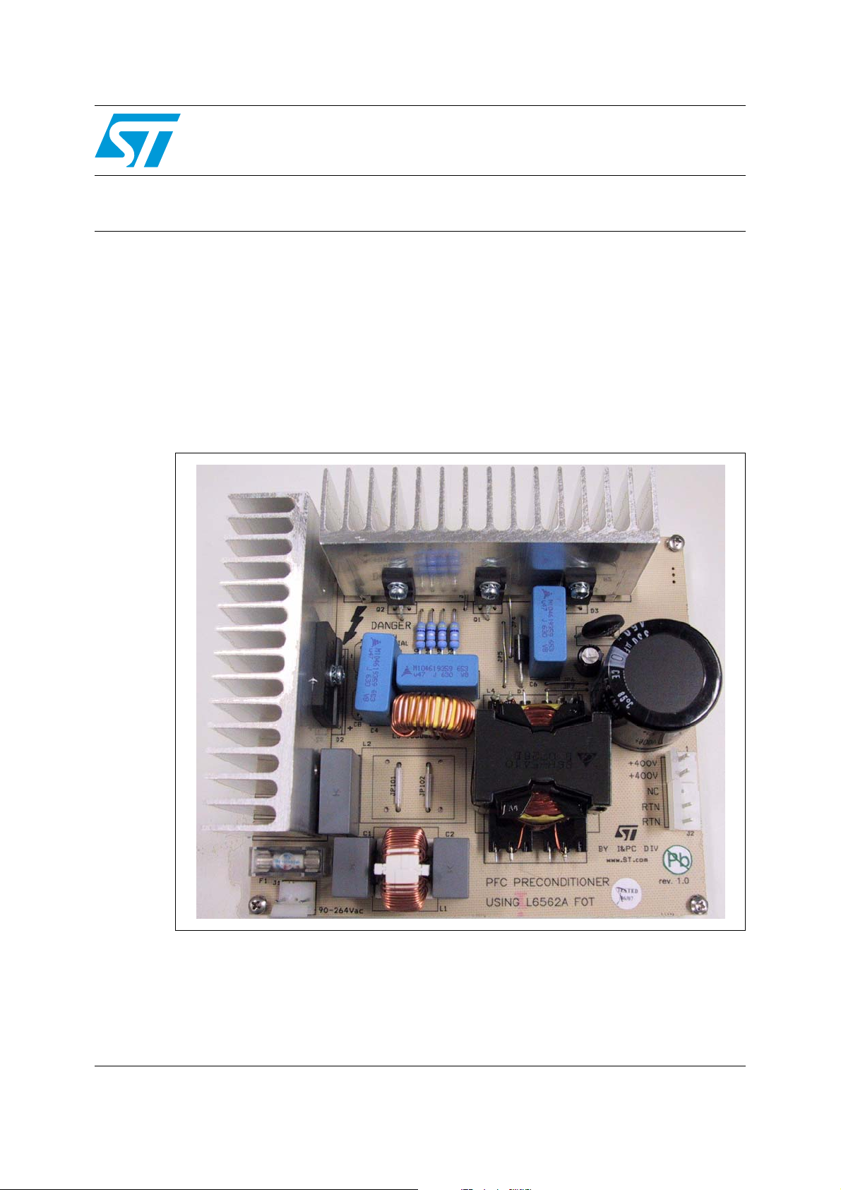
This application note describes an demonstration board based on the transition-mode PFC
controller L6562A and presents the results of its bench demonstration. The board
implements a 400 W, wide-range mains input PFC pre-conditioner suitable for ATX PSU, flat
screen displays, etc. In order to allow the use of a low-cost device like the L6562A at this
power level, usually prohibitive for this device, the chip is operated with fixed-off-time control.
This allows continuous conduction mode operation, normally achievable with more
expensive control chips and more complex control architectures.
Figure 1. Demonstration board (EVL6562A-400W)
July 2008 Rev 1 1/24
www.st.com
Page 2

Contents AN2755
Contents
1 Main characteristics and circuit description . . . . . . . . . . . . . . . . . . . . . 5
2 Test results and significant waveforms . . . . . . . . . . . . . . . . . . . . . . . . . 7
2.1 Harmonic content measurement . . . . . . . . . . . . . . . . . . . . . . . . . . . . . . . . 7
2.2 Inductor current in FOT and L6562A THD optimizer . . . . . . . . . . . . . . . . 10
2.3 Overvoltage protection and disable function . . . . . . . . . . . . . . . . . . . . . . 11
3 Layout hints . . . . . . . . . . . . . . . . . . . . . . . . . . . . . . . . . . . . . . . . . . . . . . . 12
4 Audible noise . . . . . . . . . . . . . . . . . . . . . . . . . . . . . . . . . . . . . . . . . . . . . . 13
5 Thermal measures . . . . . . . . . . . . . . . . . . . . . . . . . . . . . . . . . . . . . . . . . . 14
6 Conducted emission pre-compliance test . . . . . . . . . . . . . . . . . . . . . . 16
7 Bill of material . . . . . . . . . . . . . . . . . . . . . . . . . . . . . . . . . . . . . . . . . . . . . 17
8 PFC coil specification . . . . . . . . . . . . . . . . . . . . . . . . . . . . . . . . . . . . . . . 20
8.1 General description and characteristics . . . . . . . . . . . . . . . . . . . . . . . . . . 20
8.2 Electrical characteristics . . . . . . . . . . . . . . . . . . . . . . . . . . . . . . . . . . . . . . 20
8.3 Mechanical aspect and pin numbering . . . . . . . . . . . . . . . . . . . . . . . . . . . 21
9 References . . . . . . . . . . . . . . . . . . . . . . . . . . . . . . . . . . . . . . . . . . . . . . . . 22
10 Revision history . . . . . . . . . . . . . . . . . . . . . . . . . . . . . . . . . . . . . . . . . . . 23
2/24
Page 3

AN2755 List of tables
List of tables
Table 1. Measured temperature table at 115 Vac and 230 Vac - full load . . . . . . . . . . . . . . . . . . . . 15
Table 2. Bill of material . . . . . . . . . . . . . . . . . . . . . . . . . . . . . . . . . . . . . . . . . . . . . . . . . . . . . . . . . . . 17
Table 3. Winding characteristics . . . . . . . . . . . . . . . . . . . . . . . . . . . . . . . . . . . . . . . . . . . . . . . . . . . . 20
Table 4. Document revision history . . . . . . . . . . . . . . . . . . . . . . . . . . . . . . . . . . . . . . . . . . . . . . . . . 23
3/24
Page 4

List of figures AN2755
List of figures
Figure 1. Demonstration board (EVL6562A-400W) . . . . . . . . . . . . . . . . . . . . . . . . . . . . . . . . . . . . . . . 1
Figure 2. EVL6562A-400W demonstration board electrical schematic . . . . . . . . . . . . . . . . . . . . . . . . 6
Figure 3. EVL6562A-400W compliance to EN61000-3-2 standard at full load . . . . . . . . . . . . . . . . . 7
Figure 4. EVL6562A-400W compliance to JEIDA-MITI standard at full load . . . . . . . . . . . . . . . . . . . . 7
Figure 5. EVL6562A-400W compliance to EN61000-3-2 standard at 70 W load . . . . . . . . . . . . . . . 7
Figure 6. EVL6562A-400W compliance to JEIDA-MITI standard at 70 W load . . . . . . . . . . . . . . . . . . 7
Figure 7. EVL6562A-400W input current waveform at 100 V - 50 Hz - 400 W load . . . . . . . . . . . . . . 8
Figure 8. EVL6562A-400W input current waveform at 230 V - 50 Hz - 400 W load . . . . . . . . . . . . . . 8
Figure 9. EVL6562A-400W input current waveform at 100 V - 50 Hz - 200 W load . . . . . . . . . . . . . . 8
Figure 10. EVL6562A-400W input current waveform at 230 V - 50 Hz - 200 W load . . . . . . . . . . . . . . 8
Figure 11. EVL6562A-400W input current waveform at 100 V - 50 Hz - 70 W load . . . . . . . . . . . . . . . 8
Figure 12. EVL6562A-400W input current waveform at 230 V - 50 Hz - 70 W load . . . . . . . . . . . . . . . 8
Figure 13. Power factor vs. Vin and load . . . . . . . . . . . . . . . . . . . . . . . . . . . . . . . . . . . . . . . . . . . . . . . . 9
Figure 14. THD vs. Vin and load . . . . . . . . . . . . . . . . . . . . . . . . . . . . . . . . . . . . . . . . . . . . . . . . . . . . . . 9
Figure 15. Efficiency vs. Vin and load . . . . . . . . . . . . . . . . . . . . . . . . . . . . . . . . . . . . . . . . . . . . . . . . . . 9
Figure 16. Static Vout regulation vs. Vin and load . . . . . . . . . . . . . . . . . . . . . . . . . . . . . . . . . . . . . . . . . 9
Figure 17. EVL6562A-400W inductor current ripple envelope at 115 Vac - 60 Hz - full load . . . . . . . 10
Figure 18. EVL6562A-400W inductor current ripple (detail) at 115 Vac - 60 Hz - full load . . . . . . . . . 10
Figure 19. EVL6562A-400W inductor current ripple envelope at 230 Vac - 50 Hz - full load . . . . . . . 11
Figure 20. EVL6562A-400W Inductor current ripple (detail) at 230 Vac-50 Hz -full load. . . . . . . . . . . 11
Figure 21. EVL6562A-400W PCB layout (not scaled 1:1) . . . . . . . . . . . . . . . . . . . . . . . . . . . . . . . . . . 12
Figure 22. Thermal map at 115 Vac - 60 Hz - full load . . . . . . . . . . . . . . . . . . . . . . . . . . . . . . . . . . . . 14
Figure 23. Thermal map at 230 Vac - 50 Hz - full load . . . . . . . . . . . . . . . . . . . . . . . . . . . . . . . . . . . . 14
Figure 24. 115 Vac and full load - phase . . . . . . . . . . . . . . . . . . . . . . . . . . . . . . . . . . . . . . . . . . . . . . . 16
Figure 25. 115 Vac and full load - neutral . . . . . . . . . . . . . . . . . . . . . . . . . . . . . . . . . . . . . . . . . . . . . . 16
Figure 26. 230 Vac and full load - phase . . . . . . . . . . . . . . . . . . . . . . . . . . . . . . . . . . . . . . . . . . . . . . . 16
Figure 27. 230 Vac and full load - neutral . . . . . . . . . . . . . . . . . . . . . . . . . . . . . . . . . . . . . . . . . . . . . . 16
Figure 28. Electrical diagram . . . . . . . . . . . . . . . . . . . . . . . . . . . . . . . . . . . . . . . . . . . . . . . . . . . . . . . . 20
Figure 29. Pin side view . . . . . . . . . . . . . . . . . . . . . . . . . . . . . . . . . . . . . . . . . . . . . . . . . . . . . . . . . . . . 21
4/24
Page 5

AN2755 Main characteristics and circuit description
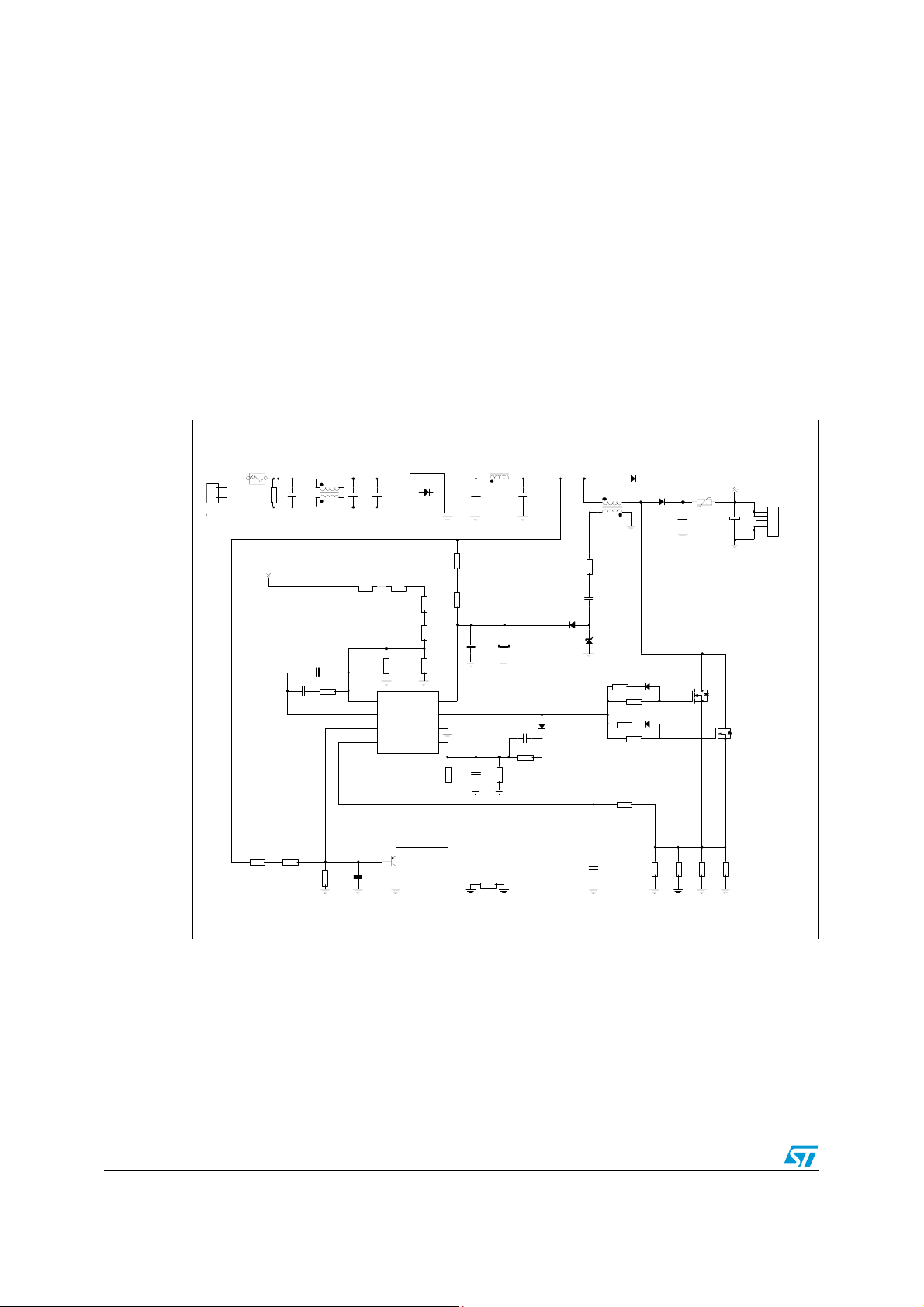
1 Main characteristics and circuit description
The main characteristics of the SMPS are listed here below:
● Line voltage range: 90 to 265 Vac
● Minimum line frequency (f
● Regulated output voltage: 400 V
● Rated output power: 400 W
● Maximum 2f
● Hold-up time: 22 ms (V
● Maximum switching frequency: 85 kHz (V
● Minimum estimated efficiency: 90 % (V
● Maximum ambient temperature: 50 °C
● EMI: In accordance with EN55022 class-B
● PCB type and size: Single side, 70 µm, CEM-1, 148.5 x 132 mm
● Low profile design: 35 mm component maximum height
output voltage ripple: 10 V pk-pk
L
The demonstration board implements a power factor correction (PFC) pre-regulator
delivering 400 W continuous power on a regulated 400 V rail from a wide-range mains
voltage and provides for the reduction of the mains harmonics, which allows meeting the
European norm EN61000-3-2 or the Japanese norm JEIDA-MITI. This rail is the input for the
cascaded isolated DC-DC converter that provides the output rails required by the load.
): 47 Hz
L
after hold-up time: 300 V)
DROP
= 90 Vac, P
in
= 90 Vac, P
in
= 400 W)
out
= 400 W)
out
The board is equipped with enough heat sinking to allow full-load operation in still air. With
an appropriate airflow and without any change in the circuit, the demonstration board can
easily deliver up to 450 W.
The controller is the L6562A (U1), integrating all the functions needed to control the PFC
stage.
The L6562A controller chip is designed for transition-mode (TM) operation, where the boost
inductor works next to the boundary between continuous (CCM) and discontinuous
conduction mode (DCM). However, with a slightly different usage, the chip can operate so
that the boost inductor works in CCM, hence surpassing the limitations of TM operation in
terms of power handling capability. The gate-drive capability of the L6562A is also adequate
to drive the MOSFETs used at higher power levels. This approach, which couples the
simplicity and cost-effectiveness of TM operation with the high-current capability of CCM
operation, is the Fixed-OFF-time (FOT) control. The control modulates the ON-time of the
power switch, while its OFF-time is kept constant. More precisely, it uses the line-modulated
FOT (LM-FOT) where the OFF-time of the power switch is not rigorously constant but is
modulated by the instantaneous mains voltage. Please refer to [2] for a detailed description
of this technique.
The power stage of the PFC is a conventional boost converter, connected to the output of
the rectifier bridge D2. It includes the coil L4, the diode D3 and the capacitors C6 and C7.
The boost switch is represented by the power mosfets Q1 and Q2. The NTC R2 limits the
inrush current at switch-on. It has been connected on the DC rail, in series to the output
electrolytic capacitor, in order to improve the efficiency during low-line operation.
Additionally, the splitting in two of output capacitors (C6 and C7) allows managing the AC
current mainly by the film capacitor C7 so that the electrolytic can be cheaper as it just has
to bear the DC part only.
5/24
Page 6
Main characteristics and circuit description AN2755
At startup the L6562A is powered by the Vcc capacitor (C12) that is charged via the
resistors R3 and R4. Then the L4 secondary winding (pins 8-11) and the charge pump
circuit (R5, C10, D5 and D4) generate the Vcc voltage powering the L6562A during normal
operation.
The divider R32, R33 and R34 provides the L6562A multiplier with the information of the
instantaneous voltage that is used to modulate the boost current. The divider R9, R10, R11,
R12 & 13 is dedicated to sense the output. The Line-Modulated FOT is obtained by the
timing generator components D6, C15, R15, C16, R16, R31, Q3.
The board is equipped with an input EMI filter designed for a 2-wire input mains plug. It is
composed of two stages, a common mode pi-filter connected at the input (C1, L1, C2, C3)
and a differential mode pi-filter after the input bridge (C4, L3, C5). It also offers the
possibility to easily connect a downstream converter.
Figure 2. EVL6562A-400W demonstration board electrical schematic
J1
1
2
90 - 265Vac
8A/250V
R32
620k
D2
C3
680nF-X2
INV
COMP
MULT
R10
510k
R12
47K
L6562A
Q3
BC857C
D15X B60
+
-~~
R102
0R0
R11
510k
R13
12k
8
VCC
7
GD
6
GND
5
ZCDCS
+400Vdc
CM-1.5mH-5A
L1
C1
R1
470nF-X2
1M5
C14
2.2uF
R33
620k
C2
470nF
R9
510k
C13
22 0nF
R14
47k
1
2
3
4
C21
R34
10nF
10k
F1
L3
DM-51uH-6A
C4
470n F-630 V
R3
100K
R4
100K
C11
470nF/50V
R31
3k
C16
120p F
R101
0R0
R16
30k
C12
100uF/50V
C15
68pF
C5
470nF-63 0V
R15
1k8
811
D4
LL4148
LL41 48
D6
5-6
T
PQ40- 500uH
R5
47R
C10
22N
D5
BZX8 5-C 18
C20
330pF
D1
1N54 06
1-2
D3
STTH8R06
C6
470nF-630V
R2
NTC 2R5-S237
330uF-450 V
+400Vdc
J2
1
+400Vdc
2
+400Vdc
3
NC
4
C7
RTN
5
RTN
+400Vout
D7
LL4148
D8
LL4148
R20
0R47-1 W
STP1 2NM50FP
R21
0R4 7-1W
Q1
Q2
STP1 2NM50FP
R22
R23
0R47-1W
0R4 7-1W
R36
3R9
R17
6R8
R35
3R9
R18
6R8
R19
1K0
6/24
Page 7
AN2755 Test results and significant waveforms
2 Test results and significant waveforms
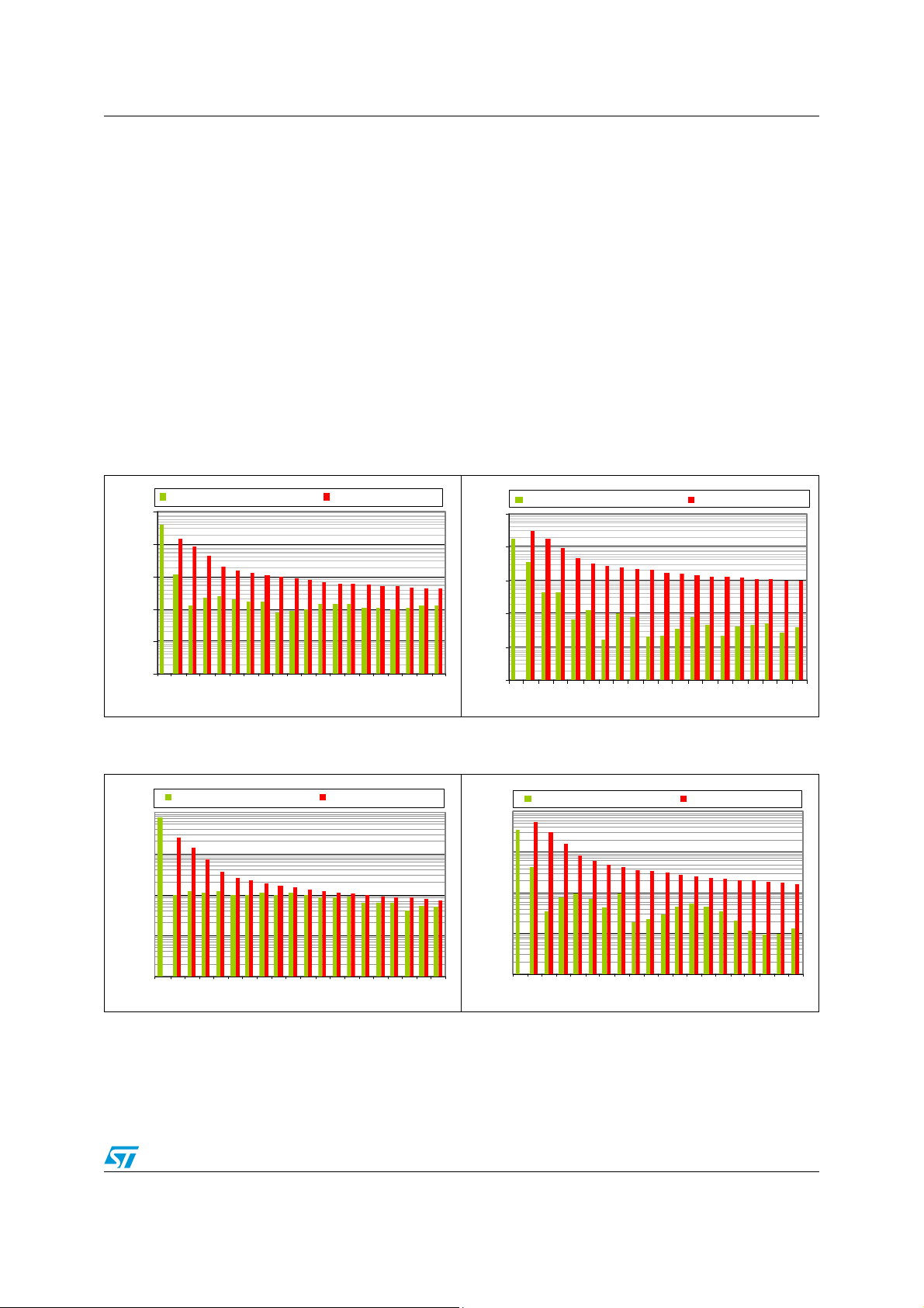
2.1 Harmonic content measurement
One of the main purposes of a PFC pre-conditioner is the correction of input current
distortion, decreasing the harmonic contents below the limits of the actual regulations.
Therefore, the board has been tested according to the European rule EN61000-3-2 class-D
and Japanese rule JEIDA-MITI class-D, at full load and 70 W output power, at both the
nominal input voltage mains.
As shown in the following figures of this page, the circuit is capable of reducing the
harmonics well below the limits of both regulations from full load down to light load. 70 W of
output power has been chosen because it approaches the lower power limit at which the
harmonics have to be limited according to the mentioned rules.
Figure 3. EVL6562A-400W compliance to
10
EN61000-3-2 standard at full load
Measurements @ 230Vac Full load EN61000-3-2 class D limits
Figure 4. EVL6562A-400W compliance to
JEIDA-MITI standard at full load
Measurements @ 100Vac Full load JEIDA-MITI class D limits
10
1
0.1
0.01
Ha rm on i c c u rr en t ( A)
0.001
0.0001
1 3 5 7 9 111315171921232527293133353739
Harmonic Order (n)
Figure 5. EVL6562A-400W compliance to
1
0.1
0.01
Harmonic current (A)
0. 00 1
0.0001
EN61000-3-2 standard at 70 W load
Measurements @ 230Vac 70W EN61000-3-2 class D limits
1 3 5 7 9 11 13 15 17 19 21 23 25 27 29 31 33 35 37 39
Harmonic Order (n)
1
0.1
0.01
Harmonic current (A)
0.001
0.0001
1 3 5 7 9111315171921232527293133353739
Harmonic Order (n)
Figure 6. EVL6562A-400W compliance to
JEIDA-MITI standard at 70 W load
Harmonic current (A)
0.001
0.0001
Measurements @ 100Vac 70W JEIDA-MITI cla ss D lim its
1
0.1
0. 01
1 3 5 7 9 1113151719 212325272931 33 3537 39
Harmonic Order (n)
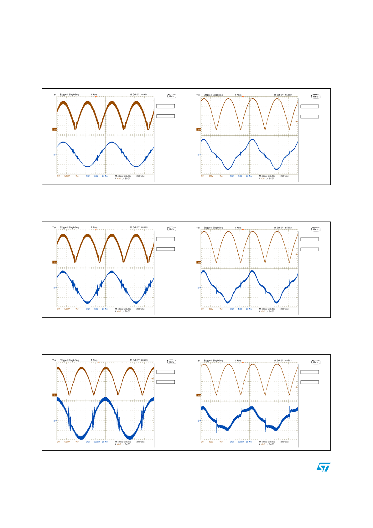
For user reference, waveforms of the input current and voltage at the nominal input voltage
mains and different load conditions are shown in the following figures.
7/24
Page 8
Test results and significant waveforms AN2755
Figure 7. EVL6562A-400W input current
waveform
at 100 V - 50 Hz - 400 W load
Figure 9. EVL6562A-400W input current
waveform
at 100 V - 50 Hz - 200 W load
Figure 8. EVL6562A-400W input current
waveform
at 230 V - 50 Hz - 400 W load
Figure 10. EVL6562A-400W input current
waveform
at 230 V - 50 Hz - 200 W load
Figure 11. EVL6562A-400W input current
waveform
8/24
at 100 V - 50 Hz - 70 W load
Figure 12. EVL6562A-400W input current
waveform
at 230 V - 50 Hz - 70 W load
Page 9

AN2755 Test results and significant waveforms
The power factor (PF) and the total harmonic distortion (THD) have been measured too and
the results are shown in Figure 13 and Figure 14. As visible, the PF at full load and half load
remains close to unity throughout the input voltage mains range while, when the circuit is
delivering 70 W, it decreases at high mains range. THD is low, remaining within 30 % at
maximum input voltage.
Figure 13. Power factor vs. Vin and load Figure 14. THD vs. Vin and load
1.05
1.00
0.95
0.90
PF
0.85
0.80
0.75
0.70
Pout = 400W
Pout = 200W
Pout = 70W
80 130 180 230 2 80
Vin (V ac)
35
30
25
20
15
TH D (%)
10
5
0
80 130 180 230 280
Vin (V ac)
Pout = 400W
Pout = 200W
Pout = 70W
The efficiency is very good at all load and line conditions. At full load it is always significantly
higher than 90%, making this design suitable for high efficiency power supply.
The measured output voltage variation at different line and load conditions is shown in
Figure 16. As visible, the voltage is perfectly stable over the input voltage range. Just at 265
Vac and light load, there are negligible deviations of 1 V due to the intervention of the burst
mode (for the "static OVP") function.
Figure 15. Efficiency vs. Vin and load Figure 16. Static Vout regulation vs. Vin and
404
403
402
401
400
Vout (V dc)
399
398
397
80 1 30 180 230 2 80
load
Pout = 400W
Pout = 200W
Pout = 70W
Pout = 15W
Vin (Va c)
9/24
Page 10

Test results and significant waveforms AN2755
2.2 Inductor current in FOT and L6562A THD optimizer
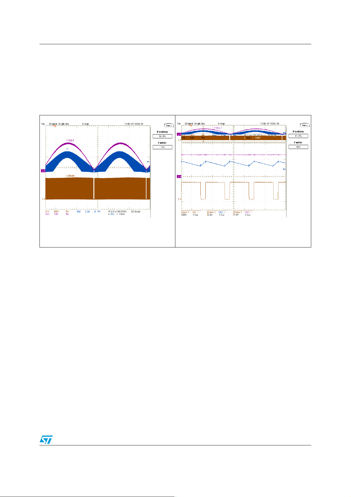
The following figures show the waveforms relevant to the inductor current at different voltage
mains. As visible in Figure 17 and Figure 19, the inductor current waveform over a line halfperiod is very similar to that of a CCM PFC. In Figure 18 and Figure 20 the magnification of
the waveforms at the peak of the sine wave shows the different ripple current and off-times,
which is modulated by the input mains voltage. We can also note the transition angle from
DCM to CCM that occurs closer to the zero-crossing of the current sine wave at low mains
and moves toward the top if the circuit is working at high mains.
Figure 17. EVL6562A-400W inductor current
ripple envelope at 115 Vac - 60 Hz -
● CH1: Q1/Q2 drain voltage
● CH2: I L inductor current ripple envelope
● CH3: MULT voltage - pin #3
full load
On both the drain voltage traces shown in Figure 17 and Figure 19, close to the zerocrossing points of the sine wave, it is possible to note the action of the THD optimizer
embedded in the L6562A. It is a circuit that minimizes the conduction dead-angle occurring
to the AC input current near the zero-crossings of the line voltage (crossover distortion). In
this way, the THD (Total Harmonic Distortion) of the current is considerably reduced. A
major cause of this distortion is the inability of the system to transfer energy effectively when
the instantaneous line voltage is very low. This effect is magnified by the high-frequency
filter capacitor placed after the bridge rectifier, which retains some residual voltage that
causes the diodes of the bridge rectifier to be reverse-biased and the input current flow to
temporarily stop. To overcome this issue the device forces the PFC pre-regulator to process
more energy near the line voltage zero-crossings as compared to that commanded by the
control loop.
Figure 18. EVL6562A-400W inductor current
ripple (detail) at 115 Vac - 60 Hz -
● CH1: Q1/Q2 drain voltage
● CH2: I L inductor current ripple envelope
● CH3: MULT voltage - pin #3
full load
This results in both minimizing the time interval where energy transfer is lacking and fully
discharging the high-frequency filter capacitor after the bridge. Essentially, the circuit
artificially increases the ON-time of the power switch with a positive offset added to the
output of the multiplier in the proximity of the line voltage zero-crossings.
This offset is reduced as the instantaneous line voltage increases, so that it becomes
negligible as the line voltage moves toward the top of the sinusoid.
10/24
Page 11
AN2755 Test results and significant waveforms
To maximally benefit from the THD optimizer circuit, the high-frequency filter capacitors after
the bridge rectifier should be minimized, compatibly with EMI filtering needs. A large
capacitance, in fact, introduces a conduction dead-angle of the AC input current in itself thus
reducing the effectiveness of the optimizer circuit.
Figure 19. EVL6562A-400W inductor current
ripple envelope at 230 Vac - 50 Hz -
● CH1: Q1/Q2 drain voltage
● CH2: I L inductor current ripple envelope
● CH3: MULT voltage - pin #3
full load
Figure 20. EVL6562A-400W Inductor current
ripple (detail) at 230 Vac-50 Hz -
● CH1: Q1/Q2 drain voltage
● CH2: I L inductor current ripple envelope
● CH3: MULT voltage - pin #3
full load
2.3 Overvoltage protection and disable function
The L6562A is equipped by an OVP, monitoring the current flowing through the
compensation network and entering in the error amplifier (pin COMP, #2). When this current
reaches about 24 µA the output voltage of the multiplier is forced to decrease, thus reducing
the energy drawn from the mains. If the current exceeds 27 µA, the OVP is triggered
(dynamic OVP), and the external power transistor is switched off until the current falls
approximately below 7 µA. However, if the overvoltage persists (e.g. in case the load is
completely disconnected), the error amplifier eventually saturates low hence triggering an
internal comparator (static OVP) that keeps the external power switch turned off until the
output voltage comes back close to the regulated value.
The OVP function described above is able to handle abnormal overload conditions, i.e.
those resulting from an abrupt load/line change or occurring at startup.
The INV pin doubles its function as a non-latched IC disable. A voltage below 0.2 V shuts
down the IC and reduces its consumption to a lower value. To restart the IC, the voltage on
the pin must exceed 0.45 V. The main usage of this function is a remote ON/OFF control
input that can be driven by a PWM controller for power management purposes. However it
also offers a certain degree of additional safety since it causes the IC to shut down in case
the lower resistor of the output divider is shorted to ground or if the upper resistor is missing
or fails to open.
11/24
Page 12

Layout hints AN2755
3 Layout hints
The layout of any converter is a very important phase in the design process that sometimes
does not have enough attention from the engineers. Even if it the layout phase sometimes
looks time-consuming, a good layout does save time during the functional debugging and
the qualification phases. Additionally, a power supply circuit with a correct layout needs
smaller EMI filters or less filter stages which allows consistent cost savings.
The L6562A does not need any special attention to the layout, just the general layout rules
for any power converter have to be carefully applied. Basic rules are listed below, using the
EVL6562A-400W schematic as a reference. They can be used for other PFC circuits having
any power level, working either in FOT or TM control.
1. Keep power and signal RTNs separated. Connect the return pins of componentcarrying high currents such as C4, C5 (input filter), sense resistors, and C6, C7 (output
capacitors) as close as possible. This point is the RTN star point. A downstream
converter must be connected to this return point.
2. Minimize the length of the traces relevant to L3, boost inductor L4, boost rectifier D4
and output capacitor C6 and C7.
3. Keep signal components as close as possible to each L6562A relevant pin. Specifically,
keep the tracks relevant to pin #1 (INV) net as short as possible. Components and
traces relevant to the error amplifier have to be placed far from traces and connections
carrying signals with high dv/dt like the MOSFET drains (Q1 and Q2).
4. Connect heat sinks to power GND.
5. Add an external shield to the boost inductor and connect it to power GND.
6. Connect a ceramic capacitor (100 ÷ 470 uF) to pin #8 (Vcc) and to pin #6 (GND) and
close to the L6562A. Connect pin #6 (GND) to the RTN star point (see 1).
Figure 21. EVL6562A-400W PCB layout (not 1:1 scaled)
PFC PRECONDITIONER
PFC PRECONDITIONER
USING L6562A FOT
USING L6562A FOT
12/24
Page 13

AN2755 Audible noise
4 Audible noise
Differential mode currents in a circuit with high-frequency and low-frequency components
(like in a PFC) may produce audible noise due to intermodulation between operating
frequency and mains line frequency.
The phenomenon is produced because of mechanical vibration of reactive components like
capacitors and inductors. Current flowing in the winding can cause the vibration of wires or
ferrite which produces buzzing noise. Therefore to avoid this noise, boost and filter inductors
have to be wound with correct wire tension, and the component has to be varnished or
dipped. Frequently, X-capacitors and filter capacitors after the bridge generate acoustic
noise because of the AC current that causes the electrodes to vibrate which produces
buzzing noise. Thus, in order to minimize the AC current, inserting a differential mode (pifilter between the bridge and the boost inductor) helps to reduce the acoustic noise and
additionally the EMI filter benefits. This type of filter decreases significantly the ripple current
that otherwise has to be filtered by the EMI filter. The capacitors to select are polypropylene,
preferably dipped type, because boxed ones are generally more at risk to generate acoustic
noise.
The grounding of the boost inductor may help, because we decrease the emissions from the
most efficient "antenna" of our circuit. In fact, in case of improper layout, some picofarads of
layout parasitic capacitance, together with the very high dV/dt of the MOSFET drain voltage,
may inject noise somewhere in the circuit.
13/24
Page 14

Thermal measures AN2755
5 Thermal measures
In order to check the design reliability, a thermal mapping by means of an IR camera was
done. Figure 22 and 23 show thermal measures on the board component side at nominal
input voltages and full load. Some pointers visible on the pictures placed across key
components show the relevant temperature. Tab l e 1 provides the correlation between
measured points and components for both thermal maps. The ambient temperature during
both measurements was 27 °C. According to these measurement results, all components of
the board are working within their temperature limits.
Figure 22. Thermal map at 115 Vac - 60 Hz - full load
80.6
°C
73.9
67.2
60.5
53.8
Figure 23. Thermal map at 230 Vac - 50 Hz - full load
47.1
40.4
33.7
26.9
79.9
°C
73.2
66.6
60.0
53.3
46.7
40.0
33.4
26.8
14/24
Page 15
AN2755 Thermal measures
Table 1. Measured temperature table at 115 Vac and 230 Vac - full load
Point Component Temperature at 115 Vac Temperature at 230 Vac
A D2 64.7 °C 51.3 °C
B Q2 76.5 °C 62.0 °C
C Q1 74.1 °C 61.9 °C
D D3 72.8 °C 65.6 °C
E C7 41.0 °C 41.5 °C
F L1 58.5 °C 43.5 °C
G L3 59.2 °C 50.6 °C
H L4 – CORE 57.0 °C 56.5 °C
I L4 - WINDING 65.1 °C 60.9 °C
15/24
Page 16

Conducted emission pre-compliance test AN2755
6 Conducted emission pre-compliance test
The following figures show the peak measurement of the conducted noise at full load and
nominal mains voltages. The limits shown in the diagrams are EN55022 class-B which is the
most popular rule for domestic equipment using a two-wire mains connection. As visible in
the diagrams, in all test conditions there is a good margin of the measures with respect to
the limits.
Figure 24. 115 Vac and full load - phase Figure 25. 115 Vac and full load - neutral
Figure 26. 230 Vac and full load - phase Figure 27. 230 Vac and full load - neutral
16/24
Page 17

AN2755 Bill of material
7 Bill of material
Table 2. Bill of material
Ref.
Des.
C1 470 nF - X2 DWG X2 film capacitor R46-I 3470--M1- ARCOTRONICS
C10 22 nF 1206 100 V SMD cercap - general purpose AVX
C11 470 nF 1206 50 V SMD cercap - general purpose AVX
C12 100 uF
C13 220 nF 0805 50 V SMD cercap - general purpose AVX
C14 2.2 uF 1206 50 V SMD cercap - general purpose AVX
C15 100 pF 0805 50 V SMD cercap - general purpose AVX
C16 120 pF 0805 50 V SMD cercap - general purpose AVX
C2 470 n F - X2 DWG X2 film capacitor R46-I 3470--M1- Arcotronics
C20 330 pF 0805 50 V SMD cercap - general purpose AVX
C21 10 nF 1206 50 V SMD cercap - general purpose AVX
C3 680 nF - X2 DWG X2 film capacitor R46-I 3680--M1- Arcotronics
C4 470 nF / 630 V DWG Film capacitor MKP - B32653A6474J EPCOS
C5 470 nF / 630 V DWG Film capacitor MKP - B32653A6474J EPCOS
C6 470 nF / 630 V DWG Film capacitor MKP- B32653A6474J EPCOS
C7 330 uF / 450 V
Part type-
part value
Case/
Package
DIA8X11
(MM)
DIA 35x35
(MM)
Description Supplier
Aluminium elcap - YXF SERIES -
105 °C
Aluminium elcap - LLS series - 85 °C Nichicon
Rubycon
C8 RES DWG
C9 RES DWG
D1 1N5406 DO-201 Standard recovery rectifier Vishay
D2 D15XB60 DWG Rectifier bridge Shindengen
D3 STTH8R06 TO-220FP Ultrafast high voltage rectifier STMicroelectronics
D4 LL4148 MINIMELF Fast switching diode
D5 BZX85-C18 MINIMELF Zener diode
D6 LL4148 MINIMELF Fast switching diode
D7 LL4148 MINIMELF Fast switching diode
D8 LL4148 MINIMELF Fast switching diode
F1 8A/250V 5x20 MM 8 A mains input fuse Wickmann
J1 3-pins conn. (central rem.) P 3.96 KK series
J2 5-pins conn. (central rem.) P 3.96 KK series
JP101 JUMPER Wire jumper
Not used -
Vishay
Molex
17/24
Page 18

Bill of material AN2755
Table 2. Bill of material (continued)
Ref.
Des.
JP102 JUMPER Wire jumper
L1 CM-1.5 mH-5 A DWG CM choke - LFR2205B Delta electronics
L2 RES DWG Not used -
L3 DM-51 uH-6 A DWG Filter inductor - LSR2306-1
L4 PQ40-500 uH DWG PFC inductor - 86H-5410B
Q1 STP12NM50FP TO-220FP N-channel power MOSFET
Q2 STP12NM50FP TO-220FP N-channel power MOSFET
Q3 BC857C SOT-23 Small signal BJT - PNP Vishay
R1 1 M5 AXIAL HV resistor
R10 510 k 1206 SMD STD film res - 1% - 250 ppm / °C
R11 510 k 1206 SMD STD film res - 1% - 250 ppm / °C
R12 47 k 0805 SMD STD film res - 1% - 250 ppm / °C
R13 12 k 0805 SMD STD film res - 1% - 250 ppm / °C
R14 47 k 0805 SMD STD film res - 5% - 250 ppm / °C
R15 1 k8 0805 SMD STD film res - 1% - 100 ppm / °C
R16 30 k 0805 SMD STD film res - 1% - 100 ppm / °C
R17 6R8 0805 SMD STD film res - 5% - 250 ppm / °C
Part type-
part value
Case/
Package
Description Supplier
Delta electronics
STMicroelectronics
BC components
R18 6R8 0805 SMD STD film res - 5% - 250 ppm / °C
R19 1 K0 1206 SMD STD film res - 5% - 250 ppm / °C
R2 NTC 2R5 DWG NTC resistor 2R5 S237 EPCOS
R20 0R47-1 W AXIAL Axial res - 5% - 250 ppm / °C
R21 0R47-1 W AXIAL Axial res - 5% - 250 ppm / °C
R22 0R47-1 W AXIAL Axial res - 5% - 250 ppm / °C
R23 0R47-1 W AXIAL Axial res- 5% - 250 ppm / °C
R25 RES 1206 Not used -
BC components
18/24
Page 19

AN2755 Bill of material
Table 2. Bill of material (continued)
Ref.
Des.
R3 100 K 1206 SMD STD film res - 5% - 250 ppm / °C
R31 3 k 0805 SMD STD film res - 1% - 100 ppm / °C
R32 620 k 1206 SMD STD film res - 5% - 250 ppm / °C
R33 620 k 1206 SMD STD film res - 5% - 250 ppm / °C
R34 10 k 1206 SMD STD film res - 5% - 250 ppm / °C
R35 3R9 0805 SMD STD film res - 5% - 250 ppm / °C
R36 3R9 0805 SMD STD film res - 5% - 250 ppm / °C
R4 100 K 1206 SMD STD film res - 5% - 250 ppm / °C
R5 47 R 1206 SMD STD film res - 5% - 250 ppm / °C
R9 510 k 1206 SMD STD film res - 1% - 250 ppm / °C
R101 0R0 1206 SMD STD film res - 5% - 250 ppm / °C
R102 0R0 1206 SMD STD film res - 5% - 250 ppm / °C
U1 L6562AD SO-8 Transition-mode PFC controller STMicroelectronics
Part type-
part value
Case/
Package
Description Supplier
BC components
19/24
Page 20

PFC coil specification AN2755
8 PFC coil specification
8.1 General description and characteristics
● Application type: consumer, home appliance
● Inductor type: open
● Coil former: vertical type, 6+6 pins
● Max. temp. rise: 45 ºC
● Max. operating ambient temperature: 60 ºC
8.2 Electrical characteristics
● Converter topology: boost PFC pre-regulator, FOT control
● Core type: PQ40-30 material grade PC44 or equivalent
● Max. operating frequency: 100 kHz
● Primary inductance: 500 µH 10 % at 1 kHz - 0.25 V
●
Primary RMS current: 4.75 A
(a)
Figure 28. Electrical diagram
5 - 6 11
Primary Auxiliary
1 - 2
Table 3. Winding characteristics
Start pins End pins
11 8 5 (spaced) Single – G2 0.28Ø Bottom
5 - 6 1 - 2 65 Multistrand – G2 Litz 0.2Ø x 30 Top
Number
of turns
Wire type
8
Wire
diameter
Notes
a. Measured between pins 1-2 and 5-6
20/24
Page 21

AN2755 PFC coil specification
0
m
4
8.3 Mechanical aspect and pin numbering
● Maximum height from PCB: 31 mm
● Ferrite: Two symmetrical half cores, PQ40-30
● Material grade: PC44 or equivalent
● Central leg air gap: ~1 mm
● Coil former type: vertical, 6+6 pins
● Pin distance: 5 mm
● Row distance: 45.5 mm
● Cut pins: 9 - 12
● External copper shield: not insulated (for EMI reasons), connected to pin 11 (GND)
Figure 29. Pin side view
27.5 mm
10 mm
BARE COPPER
SHIELD (NOT
INSULATED):
10 mm x 0.05 mm
6
5
3
2
1
57 m
7
8
9
45 mm
1
11
12
Copper shield
soldering line
Tinned copper
wire
Soldering
points
10 1 1 7 8
Manufacturer:
P/N:
Delta electronics
86H-5410B
21/24
Page 22

References AN2755
9 References
1. "L6562A transition-mode PFC controller" datasheet
2. "Design of fixed-off-time-controlled PFC pre-regulators with the L6562", AN1792
3. "EVAL6562-375W demonstration board L6562-based 375W FOT-controlled PFC preregulator" AN1895
4. "L6561, enhanced transition-mode power factor corrector”, AN966
5. “400 W FOT-controlled PFC pre-regulator with the L6563”, AN2485
22/24
Page 23

AN2755 Revision history
10 Revision history
Table 4. Document revision history
Date Revision Changes
30-Jul-2008 1 Initial release
23/24
Page 24

AN2755
Please Read Carefully:
Information in this document is provided solely in connection with ST products. STMicroelectronics NV and its subsidiaries (“ST”) reserve the
right to make changes, corrections, modifications or improvements, to this document, and the products and services described herein at any
time, without notice.
All ST products are sold pursuant to ST’s terms and conditions of sale.
Purchasers are solely responsible for the choice, selection and use of the ST products and services described herein, and ST assumes no
liability whatsoever relating to the choice, selection or use of the ST products and services described herein.
No license, express or implied, by estoppel or otherwise, to any intellectual property rights is granted under this document. If any part of this
document refers to any third party products or services it shall not be deemed a license grant by ST for the use of such third party products
or services, or any intellectual property contained therein or considered as a warranty covering the use in any manner whatsoever of such
third party products or services or any intellectual property contained therein.
UNLESS OTHERWISE SET FORTH IN ST’S TERMS AND CONDITIONS OF SALE ST DISCLAIMS ANY EXPRESS OR IMPLIED
WARRANTY WITH RESPECT TO THE USE AND/OR SALE OF ST PRODUCTS INCLUDING WITHOUT LIMITATION IMPLIED
WARRANTIES OF MERCHANTABILITY, FITNESS FOR A PARTICULAR PURPOSE (AND THEIR EQUIVALENTS UNDER THE LAWS
OF ANY JURISDICTION), OR INFRINGEMENT OF ANY PATENT, COPYRIGHT OR OTHER INTELLECTUAL PROPERTY RIGHT.
UNLESS EXPRESSLY APPROVED IN WRITING BY AN AUTHORIZED ST REPRESENTATIVE, ST PRODUCTS ARE NOT
RECOMMENDED, AUTHORIZED OR WARRANTED FOR USE IN MILITARY, AIR CRAFT, SPACE, LIFE SAVING, OR LIFE SUSTAINING
APPLICATIONS, NOR IN PRODUCTS OR SYSTEMS WHERE FAILURE OR MALFUNCTION MAY RESULT IN PERSONAL INJURY,
DEATH, OR SEVERE PROPERTY OR ENVIRONMENTAL DAMAGE. ST PRODUCTS WHICH ARE NOT SPECIFIED AS "AUTOMOTIVE
GRADE" MAY ONLY BE USED IN AUTOMOTIVE APPLICATIONS AT USER’S OWN RISK.
Resale of ST products with provisions different from the statements and/or technical features set forth in this document shall immediately void
any warranty granted by ST for the ST product or service described herein and shall not create or extend in any manner whatsoever, any
liability of ST.
ST and the ST logo are trademarks or registered trademarks of ST in various countries.
Information in this document supersedes and replaces all information previously supplied.
The ST logo is a registered trademark of STMicroelectronics. All other names are the property of their respective owners.
© 2008 STMicroelectronics - All rights reserved
STMicroelectronics group of companies
Australia - Belgium - Brazil - Canada - China - Czech Republic - Finland - France - Germany - Hong Kong - India - Israel - Italy - Japan -
Malaysia - Malta - Morocco - Singapore - Spain - Sweden - Switzerland - United Kingdom - United States of America
www.st.com
24/24
 Loading...