

Page 1
AN2753
Application note
6 W single-output VIPer17 demonstration board
Introduction
The new VIPer17 device integrates in the same package two components: an advanced
PWM controller with built-in BCD6 technology and an 800 V avalanche rugged vertical
power MOSFET. The device is suitable for offline power conversion operating either with
wide range input voltage (85 V
(85 V
265 V
advantage of using few external components compared to a discrete solution, providing
several switch mode power supply protections and very low standby consumption in no-load
condition. The device operates at fixed frequency that can be 115 kHz or 60 kHz.
Frequency jittering is implemented which helps to meet the standards regarding
electromagnetic disturbance. The protections present on the device such as overload and
output overvoltage protections, secondary winding short-circuit protection, hard transformer
saturation and brownout protections improve the reliability and safety of the design.
Moreover internal thermal shutdown and an 800 V avalanche rugged power MOSFET
improve the robustness of the system.
- 132 VAC or 175 VAC - 265 VAC). With European range input voltage (175 VAC -
AC
) the device can handle up to 10 W of output power. The proposed solution has the
AC
- 270 VAC) up to 6 W or with single range input voltage
AC
The VIPer17 demonstration board is a standard single-output isolated flyback converter that
uses all the protections mentioned above. If brownout and overvoltage protection are not
necessary, the number of external components is further reduced.
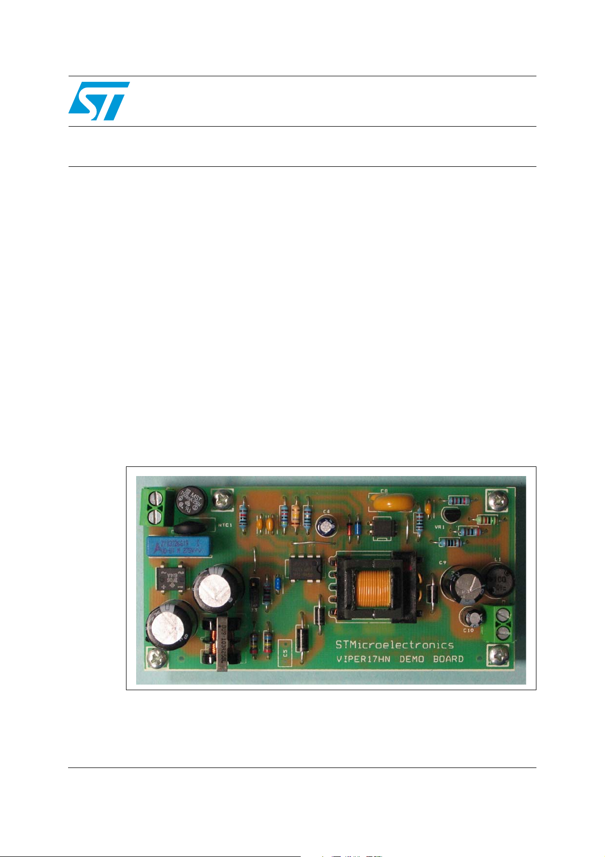
Figure 1. VIPer17HN demonstration board
Note: VIPer17HN is the full order code.
October 2009 Doc ID 14654 Rev 2 1/31
www.st.com
Page 2

Contents AN2753
Contents
1 Board description . . . . . . . . . . . . . . . . . . . . . . . . . . . . . . . . . . . . . . . . . . . 5
1.1 Transformer . . . . . . . . . . . . . . . . . . . . . . . . . . . . . . . . . . . . . . . . . . . . . . . . 8
2 Testing the board . . . . . . . . . . . . . . . . . . . . . . . . . . . . . . . . . . . . . . . . . . . 9
2.1 Typical board waveforms . . . . . . . . . . . . . . . . . . . . . . . . . . . . . . . . . . . . . . 9
3 Precision of the regulation and output voltage ripple . . . . . . . . . . . . . 11
3.1 Efficiency . . . . . . . . . . . . . . . . . . . . . . . . . . . . . . . . . . . . . . . . . . . . . . . . . 14
3.2 Light-load performance . . . . . . . . . . . . . . . . . . . . . . . . . . . . . . . . . . . . . . 17
3.3 Soft-start . . . . . . . . . . . . . . . . . . . . . . . . . . . . . . . . . . . . . . . . . . . . . . . . . . 18
3.4 Overload protection . . . . . . . . . . . . . . . . . . . . . . . . . . . . . . . . . . . . . . . . . 19
3.5 Secondary winding short-circuit protection . . . . . . . . . . . . . . . . . . . . . . . 20
3.6 Output overvoltage protection . . . . . . . . . . . . . . . . . . . . . . . . . . . . . . . . . 21
3.7 Brownout protection . . . . . . . . . . . . . . . . . . . . . . . . . . . . . . . . . . . . . . . . . 23
3.8 EMI measurements . . . . . . . . . . . . . . . . . . . . . . . . . . . . . . . . . . . . . . . . . 27
4 Conclusion . . . . . . . . . . . . . . . . . . . . . . . . . . . . . . . . . . . . . . . . . . . . . . . . 28
5 References . . . . . . . . . . . . . . . . . . . . . . . . . . . . . . . . . . . . . . . . . . . . . . . . 29
6 Revision history . . . . . . . . . . . . . . . . . . . . . . . . . . . . . . . . . . . . . . . . . . . 30
2/31 Doc ID 14654 Rev 2
Page 3

AN2753 List of tables
List of tables
Table 1. Electrical specification . . . . . . . . . . . . . . . . . . . . . . . . . . . . . . . . . . . . . . . . . . . . . . . . . . . . . 5
Table 2. Bill of materials . . . . . . . . . . . . . . . . . . . . . . . . . . . . . . . . . . . . . . . . . . . . . . . . . . . . . . . . . . . 7
Table 3. Transformer characteristics . . . . . . . . . . . . . . . . . . . . . . . . . . . . . . . . . . . . . . . . . . . . . . . . . 8
Table 4. Output voltage and V
Table 5. High frequency output voltage ripple . . . . . . . . . . . . . . . . . . . . . . . . . . . . . . . . . . . . . . . . . 11
Table 6. Burst mode related output voltage ripple . . . . . . . . . . . . . . . . . . . . . . . . . . . . . . . . . . . . . . 14
Table 7. Efficiency . . . . . . . . . . . . . . . . . . . . . . . . . . . . . . . . . . . . . . . . . . . . . . . . . . . . . . . . . . . . . . 14
Table 8. Active mode efficiencies . . . . . . . . . . . . . . . . . . . . . . . . . . . . . . . . . . . . . . . . . . . . . . . . . . . 15
Table 9. Line voltage averaged efficiency vs. load . . . . . . . . . . . . . . . . . . . . . . . . . . . . . . . . . . . . . . 16
Table 10. ENERGY STAR
Table 11. No-load input power . . . . . . . . . . . . . . . . . . . . . . . . . . . . . . . . . . . . . . . . . . . . . . . . . . . . . . 18
Table 12. Document revision history . . . . . . . . . . . . . . . . . . . . . . . . . . . . . . . . . . . . . . . . . . . . . . . . . 30
®
line-load regulation. . . . . . . . . . . . . . . . . . . . . . . . . . . . . . . . . . . . 11
DD
recommended active mode efficiency vs. Pno [1]. . . . . . . . . . . . . . . . . 17
Doc ID 14654 Rev 2 3/31
Page 4

List of figures AN2753
List of figures
Figure 1. VIPer17HN demonstration board . . . . . . . . . . . . . . . . . . . . . . . . . . . . . . . . . . . . . . . . . . . . . 1
Figure 2. Schematic . . . . . . . . . . . . . . . . . . . . . . . . . . . . . . . . . . . . . . . . . . . . . . . . . . . . . . . . . . . . . . . 6
Figure 3. Bottom view . . . . . . . . . . . . . . . . . . . . . . . . . . . . . . . . . . . . . . . . . . . . . . . . . . . . . . . . . . . . . 8
Figure 4. Side view . . . . . . . . . . . . . . . . . . . . . . . . . . . . . . . . . . . . . . . . . . . . . . . . . . . . . . . . . . . . . . . 8
Figure 5. Pins distances. . . . . . . . . . . . . . . . . . . . . . . . . . . . . . . . . . . . . . . . . . . . . . . . . . . . . . . . . . . . 8
Figure 6. Electrical diagram . . . . . . . . . . . . . . . . . . . . . . . . . . . . . . . . . . . . . . . . . . . . . . . . . . . . . . . . . 8
Figure 7. Drain current and voltage at full load and nominal input voltages (115 V
Figure 8. Drain current and voltage at full load and nominal input voltages (230 V
Figure 9. Drain current and voltage at full load and minimum input voltage (90 V
Figure 10. Drain current and voltage at full load and maximum input voltages (265 V
Figure 11. Frequency jittering (115 VIN_AC, full load) . . . . . . . . . . . . . . . . . . . . . . . . . . . . . . . . . . . . 10
Figure 12. Output voltage ripple 115 VIN_AC full load . . . . . . . . . . . . . . . . . . . . . . . . . . . . . . . . . . . . 12
Figure 13. Output voltage ripple 115 VIN_AC full load . . . . . . . . . . . . . . . . . . . . . . . . . . . . . . . . . . . . 12
Figure 14. Output voltage ripple 115 VIN_AC no load (burst mode) . . . . . . . . . . . . . . . . . . . . . . . . . . 13
Figure 15. Output voltage ripple 230 VIN_AC no load (burst mode) . . . . . . . . . . . . . . . . . . . . . . . . . . 13
Figure 16. Efficiency vs. V
. . . . . . . . . . . . . . . . . . . . . . . . . . . . . . . . . . . . . . . . . . . . . . . . . . . . . . . . . 15
IN
Figure 17. Efficiency vs. load . . . . . . . . . . . . . . . . . . . . . . . . . . . . . . . . . . . . . . . . . . . . . . . . . . . . . . . . 15
Figure 18. Active mode efficiency vs. V
Figure 19. V
Average efficiency vs. load . . . . . . . . . . . . . . . . . . . . . . . . . . . . . . . . . . . . . . . . . . . . . . 17
IN
. . . . . . . . . . . . . . . . . . . . . . . . . . . . . . . . . . . . . . . . . . . . . . 16
IN
Figure 20. Soft-start feature waveforms. . . . . . . . . . . . . . . . . . . . . . . . . . . . . . . . . . . . . . . . . . . . . . . . 18
Figure 21. Output short-circuit . . . . . . . . . . . . . . . . . . . . . . . . . . . . . . . . . . . . . . . . . . . . . . . . . . . . . . . 19
Figure 22. Operation with output shorted. . . . . . . . . . . . . . . . . . . . . . . . . . . . . . . . . . . . . . . . . . . . . . . 20
Figure 23. 2
nd
OCP protection tripping . . . . . . . . . . . . . . . . . . . . . . . . . . . . . . . . . . . . . . . . . . . . . . . . 21
Figure 24. Operating with secondary winding shorted . . . . . . . . . . . . . . . . . . . . . . . . . . . . . . . . . . . . . 21
Figure 25. OVP circuit . . . . . . . . . . . . . . . . . . . . . . . . . . . . . . . . . . . . . . . . . . . . . . . . . . . . . . . . . . . . . 22
Figure 26. OVP protection . . . . . . . . . . . . . . . . . . . . . . . . . . . . . . . . . . . . . . . . . . . . . . . . . . . . . . . . . . 23
Figure 27. OVP protection (detail) . . . . . . . . . . . . . . . . . . . . . . . . . . . . . . . . . . . . . . . . . . . . . . . . . . . . 23
Figure 28. Jumper J3 setting for brownout protection - brownout disabled . . . . . . . . . . . . . . . . . . . . . 24
Figure 29. Jumper J3 setting for brownout protection - brownout enabled . . . . . . . . . . . . . . . . . . . . . 24
Figure 30. Brownout protection block diagram . . . . . . . . . . . . . . . . . . . . . . . . . . . . . . . . . . . . . . . . . . 24
Figure 31. Brownout protection tripping . . . . . . . . . . . . . . . . . . . . . . . . . . . . . . . . . . . . . . . . . . . . . . . . 25
Figure 32. Operating with brownout protection activated. . . . . . . . . . . . . . . . . . . . . . . . . . . . . . . . . . . 26
Figure 33. Restart after brownout protection activated (detail) . . . . . . . . . . . . . . . . . . . . . . . . . . . . . . 26
Figure 34. Restart after brownout . . . . . . . . . . . . . . . . . . . . . . . . . . . . . . . . . . . . . . . . . . . . . . . . . . . . 26
Figure 35. 115 V
Figure 36. 230 V
. . . . . . . . . . . . . . . . . . . . . . . . . . . . . . . . . . . . . . . . . . . . . . . . . . . . . . . . . . . . . . . 27
AC
. . . . . . . . . . . . . . . . . . . . . . . . . . . . . . . . . . . . . . . . . . . . . . . . . . . . . . . . . . . . . . . 27
AC
) . . . . . . . . . . . . 9
AC
) . . . . . . . . . . . . 9
AC
) . . . . . . . . . . . . 9
AC
). . . . . . . . . . . 9
AC
4/31 Doc ID 14654 Rev 2
Page 5

AN2753 Board description
1 Board description
The electrical specifications of the VIPer17 demonstration board are listed in the table
below.
Table 1. Electrical specification
Parameter Symbol Value
Input voltage range V
Output voltage V
Max output current I
Precision of output regulation Δ
High frequency output voltage ripple Δ
IN
OUT
OUT
VOUT_LF
VOUT_ HF
90 V
; 265 V
RMS
12 V
500 mA
±5%
50 mV
RMS
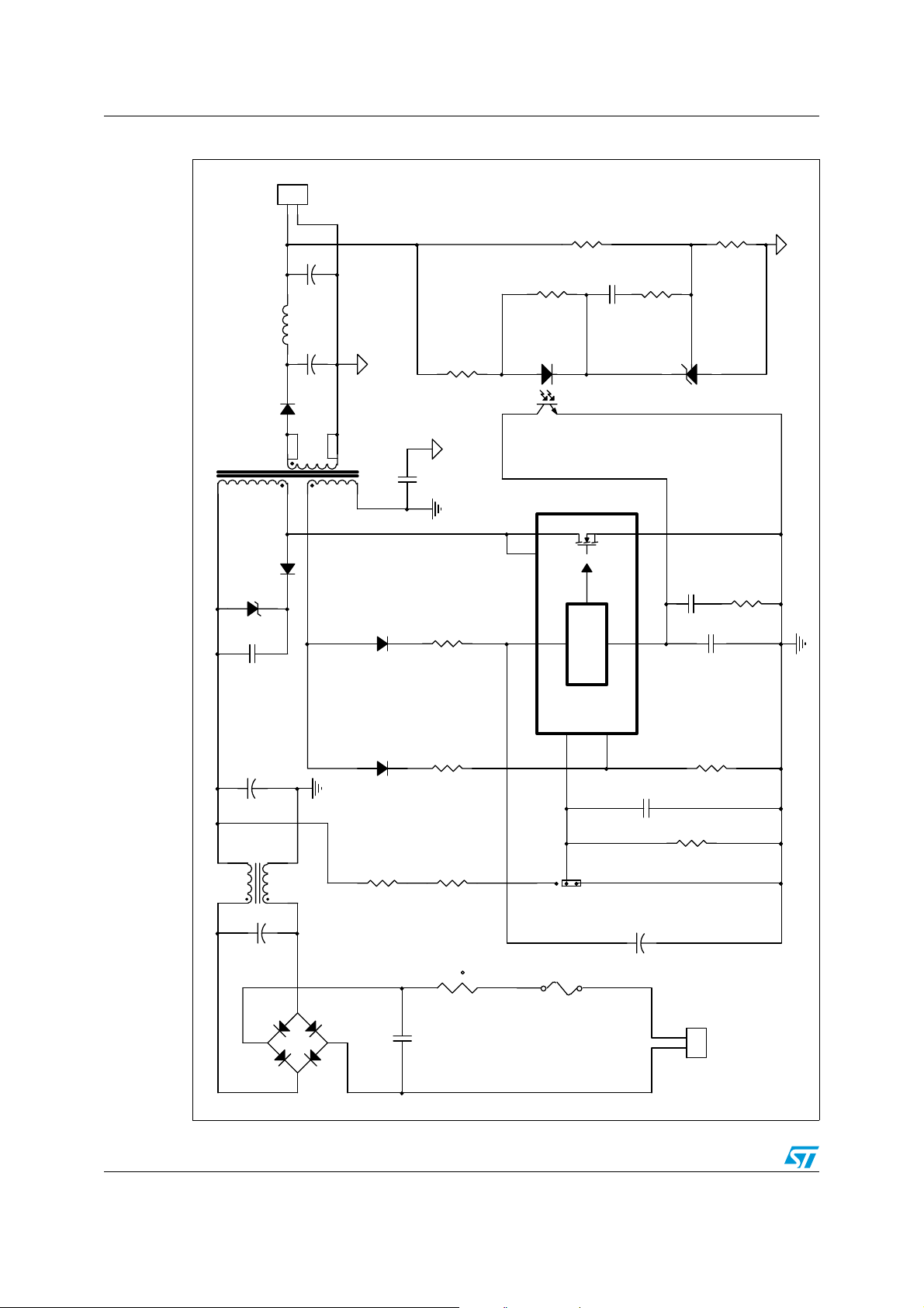
The schematics and bill of material of the board are shown in Figure 2 and Tab le 2
respectively and the transformer description is given in Tab le 3 .
In order to minimize magnetic component size, the higher operating frequency device
(VIPer17) in the DIP7 package was selected. The average switching frequency (f
SW_avg
) is
115 kHz (typ.). The switching frequency is modulated by a triangular waveform at 250 Hz
between and where Δf
(frequency jittering) spreads the spectrum of the electromagnetic interference generated by
f
SWavg
-
fmΔ=
is 8 kHz (typ.). This frequency modulation
m
the switching of the MOSFET, reducing its maximum value and facilitating compliance with
EMI standards.
In order to obtain good precision in the output regulation, a secondary regulation scheme
was used, monitoring directly the output voltage.
Thanks to the adjustable primary current limitation it is possible to fix the maximum power
that the converter can deliver to the output. The overload protection offers a good degree of
safety under output short-circuit or overload condition. As the protection is tripped the
system operates in hiccup mode reducing the power throughput to a few hundreds of
milliwatts. A second level of current limitation that latches the device if exceeded ensures
safety also in case of output diode failure (short) or secondary winding short-circuit. Output
overvoltage protection and brownout protection are also implemented. By simply changing
the position of a jumper in the board it is possible to disable the brownout protection if it is
not necessary in the specific application.
Doc ID 14654 Rev 2 5/31
Page 6
Board description AN2753
Figure 2. Schematic
1
2
J2
12V 500mA
CON2
R8
15k 1%
R9
3.9k 1%
C10
R6
L1 10uH
ZLG 47uF 25V
R13
1k
C9
1k
12
R10
C11
82k
33nF
3
VR1
TL431
2 1
43
OPTO1
PC817
81
7
DRAIN
VIPER17HN
VDD
BROWN OUT
5
U1
2
13
J3
JUMPER
F1
500mA F U SE
C7
SOURCE
FB
4 2
CONTROL
33nF
R12
10k
C6
3.3nF
CONT
3
R3
R5
47k
22k
2
1
J1 CON2
C4
C12
10nF
22uF 25V
7
4 691
ZL 470uF 25V
8
C8 Y1 1.8nF
TRANSFORMER
2
D4
STPS2H100
T1
5
D3
STTH1L06
D5
P6KE250
D1
BAT46
R1
10
C5
N.M
R14
D2
1N4148
C3
10uF 450V
4
T2
C2
2
1 3
10uF 450V
2
-+
3
BR1
1
R4
1600k
4
C1 X2
180k
R2
1600k
NTC1
10 Ohm NTC
12
t
6/31 Doc ID 14654 Rev 2
Page 7

AN2753 Board description
Table 2. Bill of materials
Item Quantity Reference Part
11BR1 Bridge
2 1 C1 EPCOS X2 100 nF MKP B32922
3 2 C2,C3 Rubycon YXA 10 µF 450 V
4 1 C4 22 µF 25 V
5 1 C5 47 pF 630 V (not mounted)
6 1 C6 3.3 nF
7 2 C7,C11 33 nF
8 1 C8 Y1 1.8 nF
9 1 C9 Rubycon ZL 470 µF 25 V
10 1 C10 Rubycon ZLG 47 µF 25V
11 1 C12 10 nF
12 1 D1 BAT46
13 1 D2 1N4148
14 1 D3 STTH1L06
15 1 D4 STPS2H100
16 1 D5 P6KE250
17 1 F1 500 mA fuse
20 1 L1 10 µH
21 1 NTC1 EPCOS B57153S0100M 10 Ω NTC
22 1 OPTO1 PC817
23 1 R1 10
24 2 R2,R4 1500 kΩ
25 1 R3 47 kΩ
26 1 R5 18 kΩ
27 2 R6,R13 1 kΩ
28 1 R8 15 kΩ 1%
29 1 R9 3.9 kΩ 1%
30 1 R10 82 kΩ
31 1 R12 10 kΩ
32 1 R14 180 kΩ
33 1 T1 Transformer
34 1 T2 Coilcraft BU9-10325BL
35 1 U1 VIPer17
36 1 VR1 TL431
Doc ID 14654 Rev 2 7/31
Page 8
Board description AN2753
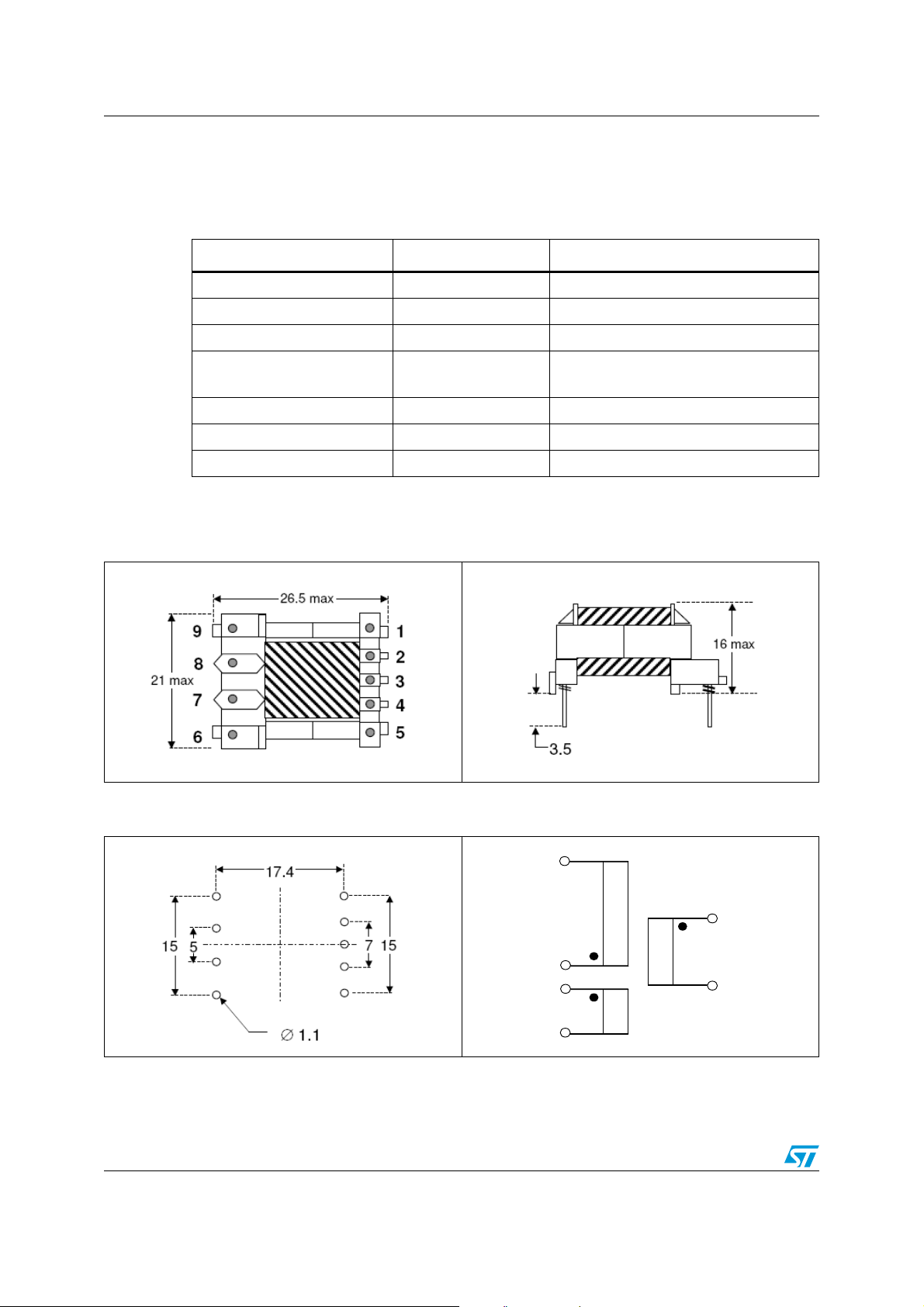
1.1 Transformer
Transformer characteristics are listed in the table below.
Table 3. Transformer characteristics
Item name Value Measure condition
Manufacturer Magnetica
Part number 1335.0034 Rev01
Primary inductance 1.2 mH +/- 15% Fr = 1 kHz, Ta = 20 °C
Leakage primary inductance 3.2% of primary
Primary to secondary turn ratio 7.85 ± 5% Fr = 10 kHz Ta = 20 °C
Primary to auxiliary turn ratio 7.85 ± 5% Fr = 10 kHz Ta = 20 °C
Insulation 4 kV Primary to secondary
Figure 3, 4, 5, 6 show size (mm), pin connection and pins distances (mm) of the transformer.
Pins 1 & 2 shorted, pins 7 & 8 shorted
Fr=10 kHz, Ta = 20 °C
Figure 3. Bottom view Figure 4. Side view
Figure 5. Pins distances Figure 6. Electrical diagram
5
A
C
4
1
2
B
7
8
8/31 Doc ID 14654 Rev 2
Page 9
AN2753 Testing the board
2 Testing the board
2.1 Typical board waveforms
The board operates with wide range input voltages and the relevant waveforms are shown
with the minimum, maximum and nominal input voltages.
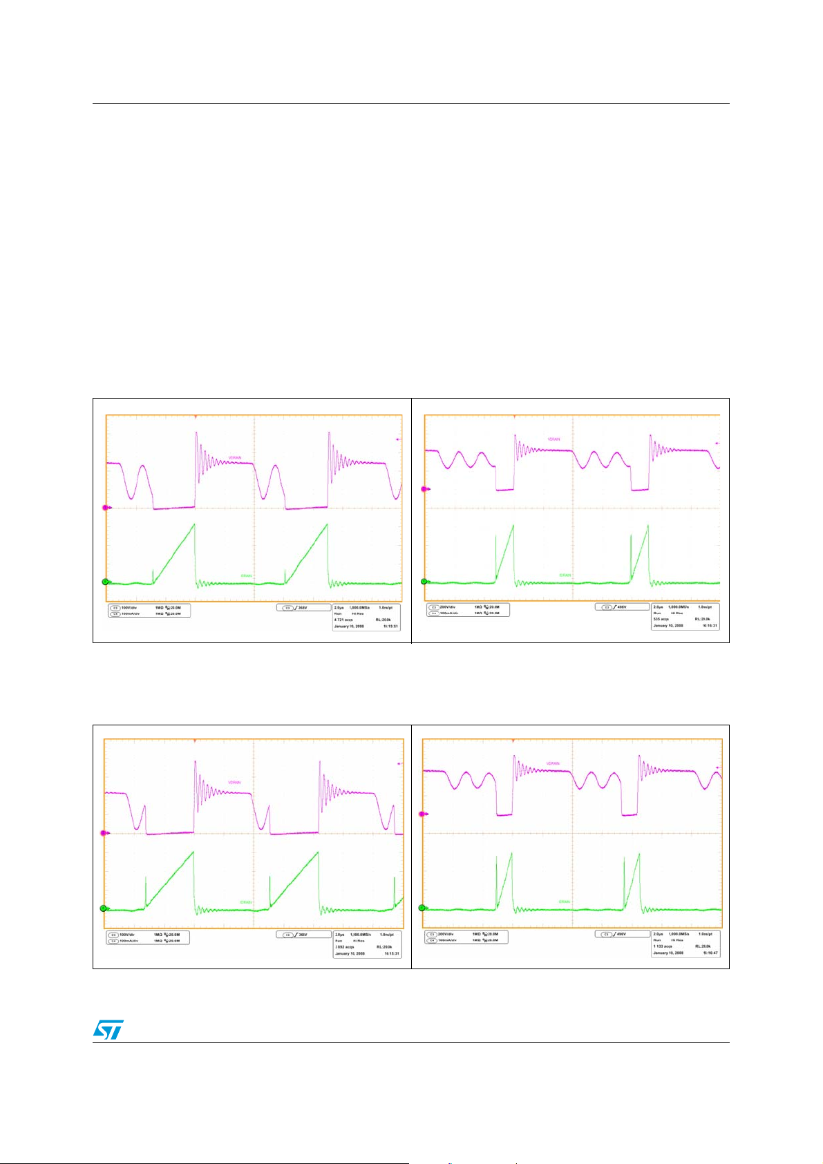
Figure 7 and Figure 8 show the drain current and the drain voltage waveforms at the
nominal input voltages, that are 115 V
(500 mA). Figure 9 and Figure 10 show the same waveforms for the same load condition,
but the input voltages are the minimum (90 V
and 230 VAC when the load is the maximum
AC
) and the maximum (265 VAC).
AC
Figure 7. Drain current and voltage at full
load and nominal input voltages
(115 V
AC
)
Figure 9. Drain current and voltage at full
load and minimum input voltage
(90 V
AC
)
Figure 8. Drain current and voltage at full
load and nominal input voltages
(230 VAC)
Figure 10. Drain current and voltage at full
load and maximum input voltages
(265 VAC)
Doc ID 14654 Rev 2 9/31
Page 10
Testing the board AN2753
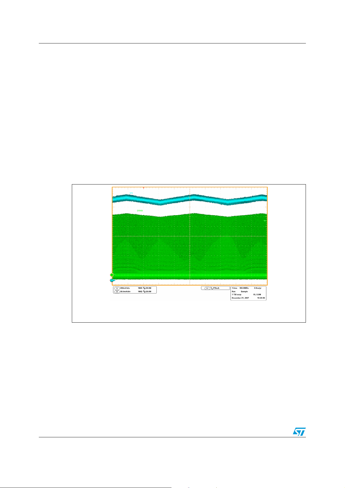
Figure 11 shows the drain current and the voltage on the feedback pin in a time interval of
about 10 ms. The system is working with a constant load but the voltage on the feedback
pin is a triangular wave shape as well as the peak drain current. These changes are the
result of the frequency jittering.
In a fixed frequency flyback converter, operating in discontinuous conduction mode, the
output power is proportional to the switching frequency according to the following formula:
Equation 1
P
OUT
1
-- -
2
2
L
I
fSWη⋅⋅ ⋅ ⋅=
PK
P
where L
is the transformer primary inductance, IPK is the drain peak current and η is the
P
converter's efficiency. The VIPer17 internal oscillator gives a switching frequency modulated
by a triangular waveform of 250 Hz (typ.). The power demand of the load is constant, but,
due to the variable switching frequency, the power delivered is not constant if I
is constant.
PK
The control loop reacts to the unsteady switching frequency, modulating the feedback pin
voltage and then, the drain peak current.
Figure 11. Frequency jittering (115 V
IN_AC
, full load)
CH2: VFB 200 mV/Div (Light blue)
CH4: I
50 mA/Div (Green)
DRAIN
Time: 1 ms/Div
10/31 Doc ID 14654 Rev 2
Page 11

AN2753 Precision of the regulation and output voltage ripple
3 Precision of the regulation and output voltage ripple
The output voltage of the board was measured in different line and load conditions. The
results are given in Ta bl e 3 . The output voltage variation range is a few mV for all tested
conditions. The V
of the device.
voltage was also measured to verify that it is inside the operating range
DD
Table 4. Output voltage and V
line-load regulation
DD
No load Half load Full load
V
(V)
INAC
V
(V) VDD (v) V
OUT
(V) VDD (V) V
OUT
(V) VDD (V)
OUT
90 12.068 10.67 12.066 19.35 12.064 21.16
115 12.068 10.60 12.066 19.33 12.064 21.23
230 12.068 10.29 12.066 19.36 12.064 21.24
265 12.068 10.21 12.066 19.28 12.064 21.22
The ripple at the switching frequency superimposed at the output voltage was also
measured. The board is provided with an LC filter to better filter the voltage ripple. The high
frequency voltage ripple across capacitor C9 (V
OUT_FLY
), that is the output capacitor of the
flyback converter before the LC filter, was also measured to verify the effectiveness of the
LC filter and for completeness of results.
Table 5. High frequency output voltage ripple
No load Half load Full load
V
(V)
INAC
90 20 150 24 508 30 520
115 22 164 24 504 40 520
230 22 200 24 512 30 524
265 26 212 24 508 32 536
V
OUT
(V) V
OUT_FLY
(V) V
OUT
(V) V
OUT_FLY
(V) V
OUT
(V) V
OUT_FLY
(V)
Waveforms of the two voltages (V
Doc ID 14654 Rev 2 11/31
OUT
and V
OUT_FLY
) are reported in Figure 12 and 13.
Page 12

Precision of the regulation and output voltage ripple AN2753
Figure 12. Output voltage ripple 115 V
CH1: V
CH2: V
(Yellow)
OUT
OUT_FLY
(Light blue)
Figure 13. Output voltage ripple 115 V
IN_AC
IN_AC
full load
full load
In the V
OUT_FLY
CH1: V
CH2: V
(CH1) waveform shown in the previous figures we see a high frequency
(Yellow)
OUT
OUT_FLY
(Light blue)
oscillation. This oscillation is due to a parasitic inductance (ESL) present in series with the
flyback output capacitor. This parasitic inductance is partially the parasitic inductance of the
capacitor itself and partially is due to the printed circuit wires.
A lower frequency ripple is present when the device is working in burst mode. In this mode
of operation the converter does not supply continuous power to its output. It alternates a
period when the power MOSFET is kept off and no power is processed by the converter and
a period when the power MOSFET is switching and power flows towards the converter
output. Even if no load is present at the output of the converter, during non-switching periods
the output capacitors are discharged by their leakage currents and by the currents needed
to supply the part of the feedback loop present at the secondary side. During the switching
period the output capacitance is recharged. Figure 14 and 15 indicate the output voltage
12/31 Doc ID 14654 Rev 2
Page 13
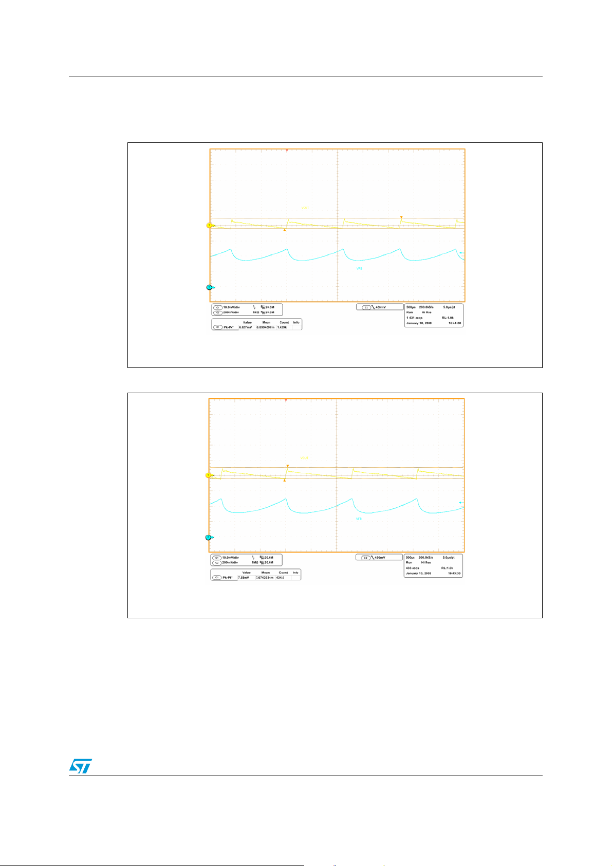
AN2753 Precision of the regulation and output voltage ripple
and the feedback voltage when the converter is not loaded. In Figure 14 the converter is
supplied with 115 V
and with 230 VAC in Figure 15.
AC
Figure 14. Output voltage ripple 115 V
CH1: V
CH2: V
(Yellow)
OUT
(Light blue)
FB
Figure 15. Output voltage ripple 230 V
no load (burst mode)
IN_AC
no load (burst mode)
IN_AC
CH1: V
CH2: V
(Yellow)
OUT
OUT_FLY
(Light blue)
Ta bl e 6 shows the measured value of the burst mode frequency ripple measured at different
operating conditions. The measured ripple in burst mode operation is very low and always
below 25 mV.
Doc ID 14654 Rev 2 13/31
Page 14

Precision of the regulation and output voltage ripple AN2753
Table 6. Burst mode related output voltage ripple
V
IN
90 6.02 8.96 10.6
115 6.63 9.68 10.4
230 7.58 11.0 13.3
265 7.35 11.8 13.6
3.1 Efficiency
The converter's efficiency is measured under different loads and input voltage operating
conditions. This efficiency was measured at full load and with 75%, 50%, and 25% with
respect to the full load condition for different input voltages applied. The results are given in
Ta bl e 7 .
Table 7. Efficiency
V
(VRMS)
INAC
90 76.92 79.62 80.76 80.32
110 79.33 80.89 81.19 79.48
115 79.75 81.03 81.19 79.48
120 80.17 81.03 81.19 79.48
No load (mV) 10 mA load (mV) 25 mA load (mV)
Efficiency (%)
Full load (0.5 A) 75% load (0.375 A) 50% load (250 mA) 25% load (125 mA)
132 80.70 81.18 80.98 78.66
175 80.91 80.60 79.71 75.17
220 79.64 79.48 77.28 71.98
230 79.33 78.93 76.50 71.31
240 79.02 78.39 74.99 70.65
265 78.11 77.33 72.93 69.05
These results were plotted in the following diagrams. In Figure 16 the efficiency versus V
IN
for four different load values was plotted. In Figure 17 the value of the efficiency versus load
for four different input voltages was plotted.
14/31 Doc ID 14654 Rev 2
Page 15

AN2753 Precision of the regulation and output voltage ripple
Figure 16. Efficiency vs. V
IN
Figure 17. Efficiency vs. load
The converter's active mode efficiency is defined as the average of the efficiencies
measured in different load conditions. These different load conditions are the 25%, 50% and
75% of maximum load and the maximum load itself. Ta b le 8 gives the active mode efficiency
calculated from the measured value in Tab le 7 . For clarity the values in Tab le 8 are plotted in
Figure 18. In Figure 19 the averaged (average was done considering the efficiency at
different input voltages) values of the efficiency versus load are shown.
Table 8. Active mode efficiencies
Active mode efficiency
V
INAC
90 79.41
110 80.22
115 80.36
120 80.47
132 80.38
Doc ID 14654 Rev 2 15/31
Efficiency
Page 16

Precision of the regulation and output voltage ripple AN2753
Table 8. Active mode efficiencies (continued)
Active mode efficiency
V
INAC
175 79.10
220 77.10
230 76.52
240 75.76
265 74.35
Figure 18. Active mode efficiency vs. V
Efficiency
IN
Table 9. Line voltage averaged efficiency vs. load
Load (% of full load) Efficiency
100 79.39
75 79.85
50 78.67
25 75.56
16/31 Doc ID 14654 Rev 2
Page 17

AN2753 Precision of the regulation and output voltage ripple
Figure 19. VIN Average efficiency vs. load
®
In order to be compliant with ENERGY STAR
recommendations regarding the efficiency in
active mode (recommendation is given in table below) the active mode efficiency has to be
higher than 65.13% (use Equation 1 considering 6 W as nameplate output power) at the
nominal input voltages (115 V
and 230 VAC in our case).
AC
Table 10. ENERGY STAR
Nameplate output power (Pno)
0 to ≤ 1 W ≥
> 1 to ≤ 49 W ≥ [0.09 * In (Pno)] + 0.49
> 49 W ≥ 0.84
®
recommended active mode efficiency vs. Pno [1]
For all the considered input voltages the efficiencyresults (see Tab l e 8 ) are higher than the
recommended value.
3.2 Light-load performance
The majority of consumer electronic manufacturers want to be compliant with the standby
mode recommendations and the device helps to achieve compliance. If the feedback pin
voltage falls below 450 mV (typ.), the MOSFET is kept off and it restarts switching when the
feedback pin voltage value exceeds 500 mV (typ.). The resulting behavior is an intermittent
working (burst mode) of the device. When the MOSFET is switching, the power delivered is
higher than necessary but it compensates the missing power during the periods where the
MOSFET is not switching. Thanks to this burst mode operation, the average switching
frequency is strongly reduced and consequently the switching losses, which are the majority
of the losses when the system is not loaded or very lightly loaded, are minimized and the
very low power consumption of the VIPer17 itself further reduces the average power that the
system has to process. The input power of the converter was measured in no-load condition
for different inputs.
Minimum average efficiency in active mode
(expressed as a decimal)
0.49 * Pno
Doc ID 14654 Rev 2 17/31
Page 18

Precision of the regulation and output voltage ripple AN2753
Table 11. No-load input power
Vin AC (VRMS) Pin (mW)
90 53
115 57
230 88
265 100
3.3 Soft-start
When the converter starts to operate, the output capacitor is totally discharged and it needs
some time to reach the nominal output power as well as the steady state condition. During
this time the power demand from the control loop is the maximum while the reflected voltage
is low. These two conditions could lead to a deep continuous operating mode of the
converter. When the MOSFET is switched on, it cannot be switched off immediately as the
minimum on time (t
because of the deep continuous working mode of the converter, during this minimum t
excess of drain current is possible which can overstress the component of the converter as
well as the device itself, the output diode, and the transformer. Transformer saturation is
also possible under these conditions.
) has to be elapsed. Even if VIPer17 has a very low minimum ton,
on
on
, an
To avoid all the described negative effects possible during the startup phase VIPer17 has on
board a soft-start feature. As the device starts to work, even if the control loop asks for the
maximum power (maximum drain current), the drain current is allowed to increase from zero
to the maximum value gradually.
The drain current limit is incremented in steps, and the values range from 0 to the fixed drain
current limitation value (value that can be adjusted through an external resistor) which is
divided in 16 steps. Each step length is 64 switching cycles. The total length of the soft-start
phase is about 8.5 ms. Figure 20 shows the soft-start phase of the presented converter
when it is operating at minimum line voltage and maximum load.
Figure 20. Soft-start feature waveforms
CH1: V
CH2: V
CH4: I
OUT
FB
DRAIN
Working conditions:
= 90V
V
IN
I
LOAD
AC
: 500 mA
18/31 Doc ID 14654 Rev 2
Page 19

AN2753 Precision of the regulation and output voltage ripple
3.4 Overload protection
If the load power demand increases, the output voltage decreases and consequently the
feedback loop reacts, increasing the voltage on the feedback pin.
The feedback pin voltage increase leads to the PWM current set point increase, with the rise
of the power delivered to the output. This process ends when the delivered power equals the
load power request.
If the load power demand exceeds the converter power capability (that can be adjusted
using R
limited to the fixed current limitation value.
), the voltage on the feedback pin continuously rises, but the drain current is
LIM
When the feedback pin voltage exceeds V
(3.3 V typ), VIPer17 assumes it to be a
FB_lin
warning status of an output overload condition. Before stopping the system, the device waits
for a time fixed by the capacitor present on the feedback pin. When the voltage on the
feedback pin exceeds V
, an internal pull-up circuit is disconnected and the pin starts
FB_lin
sourcing a 3 µA current that charges the capacitor connected to the feedback pin itself. As
the feedback pin's voltage reaches the V
stops switching and is not allowed to switch again until the V
V
DD_RESTART
(4.5 V typ.).
threshold (4.8 V typ.), the power MOSFET
FB_olp
voltage falls below
DD
The following waveform shows the behavior of the converter when the output is shorted.
Figure 21. Output short-circuit
Output shorted here
Normal operation
Over Load Delay
Stop switching
If the short-circuit is not removed, the system starts to work in auto-restart mode. The
behavior when a short-circuit is permanently applied on the output is a short period of time
where the MOSFET is switching and the converter tries to deliver to the output as much
power as it can, and a longer period where the device is not switching and no power is
processed.
If the duty cycle of power delivery is very low (around 2%), then the average power
throughput is also very low.
Doc ID 14654 Rev 2 19/31
Page 20

Precision of the regulation and output voltage ripple AN2753
Figure 22. Operation with output shorted
~ 30ms
~ 1.5s
3.5 Secondary winding short-circuit protection
The VIPer17 is provided with a first adjustable level of primary overcurrent limitation that
switches off the power MOSFET if this level is exceeded. This limitation acts cycle by cycle
and its main purpose is to limit the maximum deliverable output power. A second level of
primary overcurrent protection is also present and in this case it is fixed to 600 mA (typical
value). If the drain current exceeds this 2
nd
OCP (second overcurrent protection) threshold,
the device enters a warning state. If in the following cycle the drain current goes higher than
the second level of overcurrent protection, a secondary winding short-circuit or a hard
saturation of the transformer is assumed and the power MOSFET is no longer allowed to be
switched on. In order to enable the power MOSFET to be switched on again, the V
voltage has to be recycled which means that V
rise up to V
. When the VIPer17 is switched on again (VDD equals V
DD_ON
has to go down up to V
DD
DD_RESTART
DD_ON
DD
), the
, then
MOSFET can restart to switch. If the cause of the primary overcurrent is permanently
present, the device goes in auto-restart mode.
This protection was tested on the VIPer17 board. The secondary winding of the transformer
was shorted in different operating conditions. The following Figure 23 and 24 show the
behavior of the system during these tests.
20/31 Doc ID 14654 Rev 2
Page 21

AN2753 Precision of the regulation and output voltage ripple
Figure 23. 2nd OCP protection tripping
CH2: V
CH3: V
CH4: I
(Light blue)
FB
DRAIN
DRAIN
(Purple)
(Green)
Test condition:
V
= 11 V
IN
AC
Full load before short
In Figure 23 when the board is working in full load condition with an input voltage of 115 V
the secondary winding has been shorted. The short condition on the secondary winding
leads to high drain current. After two switching cycles, the system stops and continuous
running with high currents in the primary as well as in the secondary windings are avoided
Figure 24. Operating with secondary winding shorted
CH1: V
CH2: V
CH4: I
(Yellow)
DD
(Light blue)
FB
DRAIN
(Green)
AC
3.6 Output overvoltage protection
Monitoring the voltage across the auxiliary winding during the MOSFET off time, through the
D2 diode and the resistor divider R3 and R14 (see Figure 2) connected to the CONT pin of
the VIPer17, allows the implementation of the output overvoltage protection. If the voltage
on CONT pin exceeds the V
thresholds (3 V typ.) an overvoltage event is assumed and
OVP
Doc ID 14654 Rev 2 21/31
Test condition
=115
V
IN
Secondary winding
shorted
Page 22

Precision of the regulation and output voltage ripple AN2753
the device is no longer allowed to switch. To re-enable operation the VDD voltage has to be
recycled. In order to provide high noise immunity and to avoid that the spikes erroneously
trip the protection, a digital filter was implemented. The CONT pin has to sense a voltage
higher of V
for four consecutive cycles in a row before it stops operation.
OVP
Figure 25. OVP circuit
OCP
Daux
Auxiliary
winding
Rovp
CONT
Rlim
SOFT
START
OVP DETECTION
LOGIC
To OVP Protec t i on
Curr. Lim.
BLOCK
From Sens eF ET
Curr ent Lim i t C om p arator
+
To P WM Log ic
The value of the output voltage when the protection has to be tripped can be fixed by
properly selecting the resistor divider R2 and R14. With R2 selected and considering the
maximum power that the converter has to manage, output R14 has to be selected according
to the following formula.
Equation 2
R
OVP R14()
-
R
LIM R2()
-
-----------------------
3V
N
AUX
⎛⎞
--------------
⋅=
⎝⎠
V
N
OUTOVPVdropDovp D2()
S
– 3V–⋅
-
-
-
The protection has to be tested by disconnecting the opto-coupler from the feedback pin and
supplying the converter with a minimum load at its output. In this way the converter operates
in open loop condition and delivers the maximum power it can to output . The excess of
power with respect to the load charges the output capacitance, increasing the output voltage
until the OVP is tripped and the converter stops working.
In Figure 26 the output voltage increases as a consequence of the excess of power and the
output voltage reaches the value of 16 V when the power MOSFET stops switching. In
Figure 27 the CONT pin voltage, the drain current, and the output voltage are shown in
detail from when the converter is supplied up to when the overvoltage protection is tripped.
The crest value of the CONT pin voltage tracks the output voltage. Figure 27 shows the
detail of the last switching cycles before the protection is tripped.
If this protection is not desired, it is possible to not implement it. Not mounting diode D2 and
resistor R14 (see Figure 2) reduces the number of components.
22/31 Doc ID 14654 Rev 2
Page 23

AN2753 Precision of the regulation and output voltage ripple
Figure 26. OVP protection Figure 27. OVP protection (detail)
3.7 Brownout protection
The brownout protection is basically an unlatched device shutdown functionality whose
typical use is to sense a mains undervoltage. The VIPer17 has a pin (BR, pin 5) dedicated to
this function that must be connected to the DC HV bus. If the protection is not required, it
can be disabled by connecting the pin to ground. In the presented converter the brownout
protection is implemented but can be disabled by changing the jumper J3 (see Figure 2)
settings. The settings of the jumper J3 are shown in Figure 28 and 29. The converter's
shutdown is accomplished by means of an internal comparator internally referenced to 450
mV (typ, VBRth) that disables the PWM if the voltage applied at BR pin is below the internal
reference, as shown in Figure 30. PWM operation is re-enabled as the BR pin voltage is
more than 450 mV plus 50 mV of voltage hysteresis that ensures noise immunity. The
brownout comparator is also provided with current hysteresis. An internal 10 µA current
generator is ON as long as the voltage applied at the brownout pin is below 450 mV and is
OFF if the voltage exceeds 450 mv plus the voltage hysteresis.
Doc ID 14654 Rev 2 23/31
Page 24

Precision of the regulation and output voltage ripple AN2753
Figure 28. Jumper J3 setting for brownout
protection - brownout disabled
When the brownout protection is enabled, through a partition divider R4, R2 (RH in the block
diagram of Figure 30) and R5 (R
in Figure 30) in the schematic of Figure 2, the flyback
L
input voltage is sensed and feeds to the brownout pin.
The converter shutdown can be accomplished by means of an internal comparator internally
referenced to 450 mV (typ, V
) that disables the PWM if the voltage applied at its
BRth
externally available (non-inverting) input is below the internal reference, as shown in
Figure 30. PWM operation is re-enabled as the voltage at the non-inverting input is more
than 450 mV plus 50 mv of voltage hysteresis that ensure noise immunity. The brownout
comparator is also provided with current hysteresis. An internal 10 µA current generator is
ON as long as the voltage applied at the non-inverting input is below 450 mV and is OFF if
the voltage exceeds 450 mv plus the voltage hysteresis.
Figure 29. Jumper J3 setting for brownout
protection - brownout enabled
Figure 30. Brownout protection block diagram
HV Input bus
Rh
BR
Rl
0.1V
0.45V
15u
The current hysteresis provides an additional degree of freedom. It is possible to set the ON
threshold and the OFF threshold for the flyback input voltage separately by properly
24/31 Doc ID 14654 Rev 2
V
Vcc
+
-
+
DD
AC_OK D isable
VinOK
Page 25

AN2753 Precision of the regulation and output voltage ripple
choosing the resistors of the external divider. The following relationships can be established
for the ON (V
IN_ON
) and OFF (V
) thresholds of the input voltage:
IN_OFF
Equation 3
RHRL+
⎛⎞
-------------------- -
V
INOFFVBR
-
⋅=
⎝⎠
R
L
Equation 4
+
R
HRL
⎛⎞
where: I
and V
BR
V
INON
-
=10 µA (typ.) is the current hysteresis, Vh=50 mV (typ.) is the voltage hysteresis
h
V
+()
BRVh
-------------------- -
⎝⎠
R
=450 mV (typ.) is the brownout comparator internal reference.
R
⋅+⋅=
L
HIH
The following figures show how the brownout protection works in the VIPer17 board when
used. Figure 31 shows the behavior of the board when the input voltage is changed from 90
V
to 75 VAC with full load applied. The system stops switching and the output load, no
AC
longer supplied, decays monotonically to zero.
Figure 31. Brownout protection tripping
Figure 32 shows in the same situation the behavior of the voltage on the V
VIPer17. After the device stops switching, the V
decays to the V
DD
DD_RESTART
pin of the
DD
value
(4.5 V typ.), then the internal high voltage startup current source starts to charge the
capacitor connected at that pin (C4 in the schematic) with a constant current. When the V
voltage reaches the V
threshold, the VIPer17 is on, but it is not allowed to switch as
DD_ON
the input voltage is below the correct value.
Doc ID 14654 Rev 2 25/31
DD
Page 26

Precision of the regulation and output voltage ripple AN2753
Figure 32. Operating with brownout protection activated
Figure 33. Restart after brownout protection activated (detail)
Figure 34. Restart after brownout
26/31 Doc ID 14654 Rev 2
Page 27

AN2753 Precision of the regulation and output voltage ripple
3.8 EMI measurements
A pre-compliant test to EN55022 (Class B) European normative was also performed and the
results are shown in the two figures below.
Figure 35. 115 V
Figure 36. 230 V
AC
AC
Doc ID 14654 Rev 2 27/31
Page 28

Conclusion AN2753
4 Conclusion
A general-purpose single-output flyback converter demonstration board using the new
VIPer17 device was presented and the results show that very good efficiency can be
obtained using this new device. The various protections that this new device has on board
and the 800 V power section allow improving safety of the converter. Power consumption of
the converter in no-load condition is very low and good efficiency is obtained even in lightload condition.
28/31 Doc ID 14654 Rev 2
Page 29

AN2753 References
5 References
1. ENERGY STAR® program requirements for single voltage external AC-DC adapter
(Version 1.1)
2. VIPer17 datasheets.
Doc ID 14654 Rev 2 29/31
Page 30

Revision history AN2753
6 Revision history
Table 12. Document revision history
Date Revision Changes
12-Jun-2008 1 Initial release
19-Oct-2009 2 Modified Table 2: Bill of materials (items 2 and 21)
30/31 Doc ID 14654 Rev 2
Page 31

AN2753
Please Read Carefully:
Information in this document is provided solely in connection with ST products. STMicroelectronics NV and its subsidiaries (“ST”) reserve the
right to make changes, corrections, modifications or improvements, to this document, and the products and services described herein at any
time, without notice.
All ST products are sold pursuant to ST’s terms and conditions of sale.
Purchasers are solely responsible for the choice, selection and use of the ST products and services described herein, and ST assumes no
liability whatsoever relating to the choice, selection or use of the ST products and services described herein.
No license, express or implied, by estoppel or otherwise, to any intellectual property rights is granted under this document. If any part of this
document refers to any third party products or services it shall not be deemed a license grant by ST for the use of such third party products
or services, or any intellectual property contained therein or considered as a warranty covering the use in any manner whatsoever of such
third party products or services or any intellectual property contained therein.
UNLESS OTHERWISE SET FORTH IN ST’S TERMS AND CONDITIONS OF SALE ST DISCLAIMS ANY EXPRESS OR IMPLIED
WARRANTY WITH RESPECT TO THE USE AND/OR SALE OF ST PRODUCTS INCLUDING WITHOUT LIMITATION IMPLIED
WARRANTIES OF MERCHANTABILITY, FITNESS FOR A PARTICULAR PURPOSE (AND THEIR EQUIVALENTS UNDER THE LAWS
OF ANY JURISDICTION), OR INFRINGEMENT OF ANY PATENT, COPYRIGHT OR OTHER INTELLECTUAL PROPERTY RIGHT.
UNLESS EXPRESSLY APPROVED IN WRITING BY AN AUTHORIZED ST REPRESENTATIVE, ST PRODUCTS ARE NOT
RECOMMENDED, AUTHORIZED OR WARRANTED FOR USE IN MILITARY, AIR CRAFT, SPACE, LIFE SAVING, OR LIFE SUSTAINING
APPLICATIONS, NOR IN PRODUCTS OR SYSTEMS WHERE FAILURE OR MALFUNCTION MAY RESULT IN PERSONAL INJURY,
DEATH, OR SEVERE PROPERTY OR ENVIRONMENTAL DAMAGE. ST PRODUCTS WHICH ARE NOT SPECIFIED AS "AUTOMOTIVE
GRADE" MAY ONLY BE USED IN AUTOMOTIVE APPLICATIONS AT USER’S OWN RISK.
Resale of ST products with provisions different from the statements and/or technical features set forth in this document shall immediately void
any warranty granted by ST for the ST product or service described herein and shall not create or extend in any manner whatsoever, any
liability of ST.
ST and the ST logo are trademarks or registered trademarks of ST in various countries.
Information in this document supersedes and replaces all information previously supplied.
The ST logo is a registered trademark of STMicroelectronics. All other names are the property of their respective owners.
© 2009 STMicroelectronics - All rights reserved
STMicroelectronics group of companies
Australia - Belgium - Brazil - Canada - China - Czech Republic - Finland - France - Germany - Hong Kong - India - Israel - Italy - Japan -
Malaysia - Malta - Morocco - Philippines - Singapore - Spain - Sweden - Switzerland - United Kingdom - United States of America
www.st.com
Doc ID 14654 Rev 2 31/31
 Loading...