

Page 1

AN2751
Application note
L9952GXP power management system IC
Introduction
Today’s industrial community and car makers in particular, recognize reduced fuel
consumption and CO
As
a consequence, innovative power management solutions are mandatory in automotive
embedded systems for solving the dilemma that consists in drastically reducing the overall
quiescent current while the number of current sources is continuously increasing. In the
meantime, the increasing systems complexity made necessary to integrate advanced fail
safe functionalities in order to improve the sustainability and reliability of automotive
electronic control units.
The L9952GXP power management system IC has been developed to fulfil both demands.
It integrates all functions to build up a complete and configurable supply solution while
providing comprehensive fail safe functionality.
The following product and application guide can be considered as a “cookbook” for
designing L9952GXP power management based solutions. It is intended to help system,
hardware and software developers to enhance, optimize and secure their applications.
emission as a competitive and differentiating advantage.
2
This document will first introduce the key features and the main modes for operating a
standard system. Advanced options and configurations will then be introduced for
addressing more complex requirements. Finally the appendix will cover specific
configuration scenarios and diagnostic procedures that need to be carefully handled in order
to avoid any undesirable side effects. The L9952GXP software drivers have also been
inserted in appendix for a faster and more effective handling of your system.
July 2008 Rev 1 1/91
www.st.com
Page 2

Contents AN2751
Contents
1 System description . . . . . . . . . . . . . . . . . . . . . . . . . . . . . . . . . . . . . . . . . . 9
1.1 Internal block diagram . . . . . . . . . . . . . . . . . . . . . . . . . . . . . . . . . . . . . . . 10
1.2 Key features . . . . . . . . . . . . . . . . . . . . . . . . . . . . . . . . . . . . . . . . . . . . . . . 11
1.3 Standard system configuration . . . . . . . . . . . . . . . . . . . . . . . . . . . . . . . . . 11
2 Operating modes . . . . . . . . . . . . . . . . . . . . . . . . . . . . . . . . . . . . . . . . . . . 13
3 Initialization . . . . . . . . . . . . . . . . . . . . . . . . . . . . . . . . . . . . . . . . . . . . . . . 15
3.1 Power-on . . . . . . . . . . . . . . . . . . . . . . . . . . . . . . . . . . . . . . . . . . . . . . . . . 15
3.2 NReset generation . . . . . . . . . . . . . . . . . . . . . . . . . . . . . . . . . . . . . . . . . . 16
3.2.1 Power-on: cold start detection . . . . . . . . . . . . . . . . . . . . . . . . . . . . . . . . 17
3.2.2 Failure detection . . . . . . . . . . . . . . . . . . . . . . . . . . . . . . . . . . . . . . . . . . 17
3.2.3 Wake-up source identification . . . . . . . . . . . . . . . . . . . . . . . . . . . . . . . . 18
3.2.4 Microcontroller RAM integrity . . . . . . . . . . . . . . . . . . . . . . . . . . . . . . . . . 18
3.3 User defined initialization . . . . . . . . . . . . . . . . . . . . . . . . . . . . . . . . . . . . . 19
4 Watchdog operation . . . . . . . . . . . . . . . . . . . . . . . . . . . . . . . . . . . . . . . . 20
4.1 Initialization - Long Open Window (LOWi) . . . . . . . . . . . . . . . . . . . . . . . . 20
4.2 Normal operation - window watchdog . . . . . . . . . . . . . . . . . . . . . . . . . . . 21
4.3 Watchdog fail . . . . . . . . . . . . . . . . . . . . . . . . . . . . . . . . . . . . . . . . . . . . . . 22
5 Outputs control . . . . . . . . . . . . . . . . . . . . . . . . . . . . . . . . . . . . . . . . . . . . 23
5.1 Outputs descriptions . . . . . . . . . . . . . . . . . . . . . . . . . . . . . . . . . . . . . . . . 23
5.1.1 Voltage regulator V1 . . . . . . . . . . . . . . . . . . . . . . . . . . . . . . . . . . . . . . . 23
5.1.2 Voltage regulator V2 . . . . . . . . . . . . . . . . . . . . . . . . . . . . . . . . . . . . . . . 23
5.1.3 High-side drivers . . . . . . . . . . . . . . . . . . . . . . . . . . . . . . . . . . . . . . . . . . 24
5.1.4 Low-side drivers . . . . . . . . . . . . . . . . . . . . . . . . . . . . . . . . . . . . . . . . . . . 25
5.1.5 Digital outputs . . . . . . . . . . . . . . . . . . . . . . . . . . . . . . . . . . . . . . . . . . . . 25
5.2 Outputs control after power-on . . . . . . . . . . . . . . . . . . . . . . . . . . . . . . . . . 25
5.3 Fail Safe Output (FSO) . . . . . . . . . . . . . . . . . . . . . . . . . . . . . . . . . . . . . . . 26
6 Wake-up inputs . . . . . . . . . . . . . . . . . . . . . . . . . . . . . . . . . . . . . . . . . . . . 28
6.1 Cyclic contact sense . . . . . . . . . . . . . . . . . . . . . . . . . . . . . . . . . . . . . . . . . 28
2/91
Page 3

AN2751 Contents
6.2 Static contact sense . . . . . . . . . . . . . . . . . . . . . . . . . . . . . . . . . . . . . . . . . 30
7 Diagnosis . . . . . . . . . . . . . . . . . . . . . . . . . . . . . . . . . . . . . . . . . . . . . . . . . 32
7.1 Initialization diagnosis . . . . . . . . . . . . . . . . . . . . . . . . . . . . . . . . . . . . . . . 32
7.1.1 Cold start diagnosis . . . . . . . . . . . . . . . . . . . . . . . . . . . . . . . . . . . . . . . . 34
7.1.2 Vs power supply: under/over-voltage detection . . . . . . . . . . . . . . . . . . . 34
7.1.3 V1,2 voltage regulators–failing supply detection . . . . . . . . . . . . . . . . . . 35
7.1.4 NReset generation . . . . . . . . . . . . . . . . . . . . . . . . . . . . . . . . . . . . . . . . . 35
7.2 Output drivers diagnosis . . . . . . . . . . . . . . . . . . . . . . . . . . . . . . . . . . . . . . 36
7.3 Junction temperature diagnosis . . . . . . . . . . . . . . . . . . . . . . . . . . . . . . . . 37
7.4 Global error flag . . . . . . . . . . . . . . . . . . . . . . . . . . . . . . . . . . . . . . . . . . . . 37
7.5 Periodical monitoring . . . . . . . . . . . . . . . . . . . . . . . . . . . . . . . . . . . . . . . . 38
8 Standby modes . . . . . . . . . . . . . . . . . . . . . . . . . . . . . . . . . . . . . . . . . . . . 39
8.1 Preparation before entering standby modes . . . . . . . . . . . . . . . . . . . . . . 39
8.1.1 Wake-up sources . . . . . . . . . . . . . . . . . . . . . . . . . . . . . . . . . . . . . . . . . . 39
8.1.2 Contact sense flowchart . . . . . . . . . . . . . . . . . . . . . . . . . . . . . . . . . . . . 40
8.1.3 Read and store input status . . . . . . . . . . . . . . . . . . . . . . . . . . . . . . . . . . 42
8.1.4 Configure inputs . . . . . . . . . . . . . . . . . . . . . . . . . . . . . . . . . . . . . . . . . . . 42
8.1.5 Set ICMP = 0 . . . . . . . . . . . . . . . . . . . . . . . . . . . . . . . . . . . . . . . . . . . . . 44
8.1.6 Turn-Off outputs . . . . . . . . . . . . . . . . . . . . . . . . . . . . . . . . . . . . . . . . . . . 44
8.1.7 Trigger watchdog . . . . . . . . . . . . . . . . . . . . . . . . . . . . . . . . . . . . . . . . . . 44
8.2 Go to standby mode . . . . . . . . . . . . . . . . . . . . . . . . . . . . . . . . . . . . . . . . . 44
8.3 Current monitoring in V1_standby . . . . . . . . . . . . . . . . . . . . . . . . . . . . . . 46
8.3.1 Wake-up from Vbat_standby . . . . . . . . . . . . . . . . . . . . . . . . . . . . . . . . . 50
8.4 Wake-up from V1_standby . . . . . . . . . . . . . . . . . . . . . . . . . . . . . . . . . . . . 54
8.4.1 Wake-up with NReset generation . . . . . . . . . . . . . . . . . . . . . . . . . . . . . 54
8.4.2 Wake-up without NReset generation . . . . . . . . . . . . . . . . . . . . . . . . . . . 56
9 Digital outputs . . . . . . . . . . . . . . . . . . . . . . . . . . . . . . . . . . . . . . . . . . . . . 62
9.1 Looping WU inputs in V1_standby mode . . . . . . . . . . . . . . . . . . . . . . . . . 62
9.1.1 Static filter on WU3 rising-edge . . . . . . . . . . . . . . . . . . . . . . . . . . . . . . . 63
9.1.2 Static filter on WU3 falling-edge . . . . . . . . . . . . . . . . . . . . . . . . . . . . . . . 64
9.1.3 Static filter on WU4 falling-edge . . . . . . . . . . . . . . . . . . . . . . . . . . . . . . . 65
9.1.4 Timer 1 filter on WU3 and WU4 . . . . . . . . . . . . . . . . . . . . . . . . . . . . . . . 65
9.1.5 Timer 2 filter on WU3 and WU4 . . . . . . . . . . . . . . . . . . . . . . . . . . . . . . . 67
3/91
Page 4

Contents AN2751
9.1.6 Timer 1 filter on WU3 and timer 2 filter on WU4 . . . . . . . . . . . . . . . . . . 68
9.2 Looping HS open-load status . . . . . . . . . . . . . . . . . . . . . . . . . . . . . . . . . . 69
9.2.1 Timer 1 filter on HS_Out open-load . . . . . . . . . . . . . . . . . . . . . . . . . . . . 69
9.2.2 Timer 2 filter on HS_Out open-load . . . . . . . . . . . . . . . . . . . . . . . . . . . . 69
9.3 Interrupt mode . . . . . . . . . . . . . . . . . . . . . . . . . . . . . . . . . . . . . . . . . . . . . 70
10 Tips and tricks . . . . . . . . . . . . . . . . . . . . . . . . . . . . . . . . . . . . . . . . . . . . . 76
10.1 How to clear LIN and INH status bits (SR0, D17, D18) . . . . . . . . . . . . . . 76
10.2 Switch watchdog from window mode to continuous time-out mode (for
Flashing of microcontroller) 76
10.3 Border conditions to be considered when going to standby . . . . . . . . . . . 76
10.3.1 Go_V1_standby after 8x watchdog failure . . . . . . . . . . . . . . . . . . . . . . . 76
10.3.2 Go_V1_standby with watchdog failure and INT mode enabled . . . . . . . 76
10.4 Consequences of using ICMP bit . . . . . . . . . . . . . . . . . . . . . . . . . . . . . . . 76
10.5 Recommended setup on unused pins . . . . . . . . . . . . . . . . . . . . . . . . . . . 77
Appendix A L9952GXP software drivers . . . . . . . . . . . . . . . . . . . . . . . . . . . . . . . 78
Appendix B L9952GXP information summary . . . . . . . . . . . . . . . . . . . . . . . . . . . 85
Reference documents . . . . . . . . . . . . . . . . . . . . . . . . . . . . . . . . . . . . . . . . . . . . .89
Revision history . . . . . . . . . . . . . . . . . . . . . . . . . . . . . . . . . . . . . . . . . . . . . . . . . . 90
4/91
Page 5

AN2751 List of tables
List of tables
Table 1. Vbat_standby: wake-up sources list . . . . . . . . . . . . . . . . . . . . . . . . . . . . . . . . . . . . . . . . . . 50
Table 2. V1_standby: wake-up sources list . . . . . . . . . . . . . . . . . . . . . . . . . . . . . . . . . . . . . . . . . . . 54
Table 3. Unused pins recommendation . . . . . . . . . . . . . . . . . . . . . . . . . . . . . . . . . . . . . . . . . . . . . . 77
Table 4. L9952GXP information summary . . . . . . . . . . . . . . . . . . . . . . . . . . . . . . . . . . . . . . . . . . . . 85
Table 5. Reference documents. . . . . . . . . . . . . . . . . . . . . . . . . . . . . . . . . . . . . . . . . . . . . . . . . . . . . 89
Table 6. Document revision history . . . . . . . . . . . . . . . . . . . . . . . . . . . . . . . . . . . . . . . . . . . . . . . . . 90
5/91
Page 6

List of figures AN2751
List of figures
Figure 1. Door module system partitioning . . . . . . . . . . . . . . . . . . . . . . . . . . . . . . . . . . . . . . . . . . . . . 9
Figure 2. Internal block diagram . . . . . . . . . . . . . . . . . . . . . . . . . . . . . . . . . . . . . . . . . . . . . . . . . . . . 10
Figure 3. Standard system configuration . . . . . . . . . . . . . . . . . . . . . . . . . . . . . . . . . . . . . . . . . . . . . . 12
Figure 4. Correct signal behaviour at power-on . . . . . . . . . . . . . . . . . . . . . . . . . . . . . . . . . . . . . . . . . 15
Figure 5. NReset generation and handling overview . . . . . . . . . . . . . . . . . . . . . . . . . . . . . . . . . . . . . 16
Figure 6. V1 voltage regulator drop . . . . . . . . . . . . . . . . . . . . . . . . . . . . . . . . . . . . . . . . . . . . . . . . . . 19
Figure 7. Power-on behaviour: LOWi failed . . . . . . . . . . . . . . . . . . . . . . . . . . . . . . . . . . . . . . . . . . . . 20
Figure 8. Power-on procedure without watchdog trigger . . . . . . . . . . . . . . . . . . . . . . . . . . . . . . . . . . 21
Figure 9. Windows watchdog and trigger timing areas . . . . . . . . . . . . . . . . . . . . . . . . . . . . . . . . . . . 22
Figure 10. Out_HS current limitation in auto recovery mode . . . . . . . . . . . . . . . . . . . . . . . . . . . . . . . . 24
Figure 11. LS output behaviour at failing watchdog. . . . . . . . . . . . . . . . . . . . . . . . . . . . . . . . . . . . . . . 26
Figure 12. FSO behaviour after LOWi failure, forced Vbat_standby and wake-up event . . . . . . . . . . 27
Figure 13. Cyclic contact sense: contact connection . . . . . . . . . . . . . . . . . . . . . . . . . . . . . . . . . . . . . . 29
Figure 14. Cyclic contacts sense: wake-up events . . . . . . . . . . . . . . . . . . . . . . . . . . . . . . . . . . . . . . . 29
Figure 15. Static contact sense . . . . . . . . . . . . . . . . . . . . . . . . . . . . . . . . . . . . . . . . . . . . . . . . . . . . . . 30
Figure 16. Static wake-up by active-high contacts. . . . . . . . . . . . . . . . . . . . . . . . . . . . . . . . . . . . . . . . 31
Figure 17. Static wake-up by active-low contacts . . . . . . . . . . . . . . . . . . . . . . . . . . . . . . . . . . . . . . . . 31
Figure 18. Power-on diagnosis - detailed flowchart . . . . . . . . . . . . . . . . . . . . . . . . . . . . . . . . . . . . . . . 33
Figure 19. Voltage thresholds and NReset generation . . . . . . . . . . . . . . . . . . . . . . . . . . . . . . . . . . . . 36
Figure 20. Fast capture of L9952GXP global error flag . . . . . . . . . . . . . . . . . . . . . . . . . . . . . . . . . . . . 37
Figure 21. Preparation for standby flowchart . . . . . . . . . . . . . . . . . . . . . . . . . . . . . . . . . . . . . . . . . . . . 41
Figure 22. WU inputs pins configuration for active and standby modes . . . . . . . . . . . . . . . . . . . . . . . 43
Figure 23. Entering V1_standby mode procedure . . . . . . . . . . . . . . . . . . . . . . . . . . . . . . . . . . . . . . . . 45
Figure 24. Remaining in V1_standby in case of µC activity period <TCW. . . . . . . . . . . . . . . . . . . . . . 46
Figure 25. Wake-up from V1_standby by SPI access after Iv1 >Icmp_rise . . . . . . . . . . . . . . . . . . . . . 47
Figure 26. Wake-up from V1_standby by WU event after Iv1 > Icmp_rise – No NReset issued . . . . . 48
Figure 27. Wake-up from V1_standby after Iv1 > Icmp_rise followed by a watchdog failure . . . . . . . 50
Figure 28. Flowchart: wake-up from Vbat_standby or V1_standby after NReset . . . . . . . . . . . . . . . . 51
Figure 29. Wake-up from Vbat_standby mode . . . . . . . . . . . . . . . . . . . . . . . . . . . . . . . . . . . . . . . . . . 52
Figure 30. Vbat wake-up outputs behaviour . . . . . . . . . . . . . . . . . . . . . . . . . . . . . . . . . . . . . . . . . . . . 53
Figure 31. Wake-up from V1_standby mode / NReset generated . . . . . . . . . . . . . . . . . . . . . . . . . . . . 55
Figure 32. V1 wake-up: outputs and FSO behaviour. . . . . . . . . . . . . . . . . . . . . . . . . . . . . . . . . . . . . . 56
Figure 33. Wake-up from V1_standby mode without NReset generation . . . . . . . . . . . . . . . . . . . . . . 56
Figure 34. Wake-up from V1_standby by LIN (dominant to recessive) with/without pull-up . . . . . . . . 58
Figure 35. Wake-up from V1_standby by LIN (recessive to dominant) with/without pull up . . . . . . . . 59
Figure 36. Wake-up from V1_standby by CAN or LIN – NReset blockage . . . . . . . . . . . . . . . . . . . . . 60
Figure 37. LIN RxD peak after wake-up by CAN . . . . . . . . . . . . . . . . . . . . . . . . . . . . . . . . . . . . . . . . . 61
Figure 38. V1_standby DO looping - WU3 rising-edge event in static filtering . . . . . . . . . . . . . . . . . . 63
Figure 39. V1_standby DO looping – WU3 falling-edge event in static filtering. . . . . . . . . . . . . . . . . . 64
Figure 40. V1_standby DO looping – WU4 falling-edge event in static filtering. . . . . . . . . . . . . . . . . . 65
Figure 41. V1_standby DO looping – WU3 and WU4 filters in timer 1 mode. . . . . . . . . . . . . . . . . . . . 66
Figure 42. V1_standby DO looping – WU3 and WU4 filters in timer 2 mode. . . . . . . . . . . . . . . . . . . . 67
Figure 43. V1_standby DO looping - WU3 filter in timer 1 and WU4 filter in timer 2 mode . . . . . . . . . 68
Figure 44. V1_standby open-load looping (outs in timer 1 mode, open-load at out 2) . . . . . . . . . . . . 69
Figure 45. V1_standby open-load looping (outs in timer 2 mode, no open-load) . . . . . . . . . . . . . . . . 70
Figure 46. Wake-up from V1_standby mode in interrupt mode . . . . . . . . . . . . . . . . . . . . . . . . . . . . . . 71
Figure 47. V1_standby in INT mode: wake-up by V1 current monitoring. . . . . . . . . . . . . . . . . . . . . . . 72
Figure 48. V1_standby in INT mode: wake-up by V1 current monitoring. . . . . . . . . . . . . . . . . . . . . . . 73
Figure 49. Wake-up form V1_standby in interrupt mode . . . . . . . . . . . . . . . . . . . . . . . . . . . . . . . . . . . 74
Figure 50. Wake-up form V1_standby in interrupt mode by V1 current monitoring . . . . . . . . . . . . . . . 75
6/91
Page 7

AN2751 List of abbreviations
List of abbreviations
CAN Controller Area Network
CR Control Register
CSN Chip Select inverted signal of SPI
DI SPI Data-In
Dig_Out3 Digital output 3 of the L9952GXP
Dig_Out4 Digital output 4 of the L9952GXP
DO SPI Data-Out
ECU Electronic Control Unit
FSO Fail Safe Output
HS High-Side driver output
I
CMP
INH Inhibit input of L9952GXP designed for connection with CAN controller
LIN 2.1 Local Interconnect Network version 2.1 (SAEJ2602 compatible)
LINPU Local Interconnect Network Pull-Up
LOWi Long Open Window
LS Low-Side Driver Output
MISO SPI-Master In Slave Out
MOSI SPI-Master Out Slave In
NReset Active low Reset output signal - connected to microcontroller.
OC Over-Current detection
OL Open-load detection
OP Operational sense amplifier
OV Over-voltage failure of V
POR Power-On Reset
PWM Pulse Width Modulation signal
REL Relay Output-e.g. low side driver
SPI Serial Peripheral Interface
Current supervision of V1 regulator in V1_standby mode
S
SR Status Register
TRIG Trigger bit to be inverted within a Window Watchdog
TSD Thermal Shutdown
TW Temperature Warning
UV Under-Voltage failure of V
S
7/91
Page 8

List of abbreviations AN2751
Vbat_standby Vbat_standby mode
V1_standby V1_standby mode
WDC Watchdog Counter
WD Watchdog
WU Wakeup input of the L9952GXP
WU1..4 All 4 wakeup inputs of the L9952GXP
8/91
Page 9
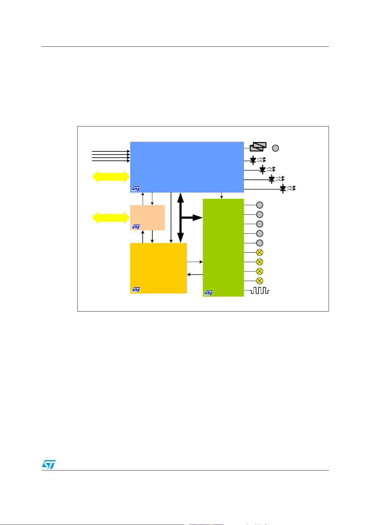
AN2751 System description
1 System description
The L9952GXP is specified for targeting microcontroller based automotive applications such
as door modules, body control units and mechatronic subsystems. Thanks to its advanced
functionality and wide ranging configuration possibilities, this power management system IC
could either address automotive embedded applications than industrial ones.
Figure 1. Door module system partitioning
Contact
Monitoring
M
Power Window
L9952GXP
LIN
CAN
Power Management System Device
CAN
Transceiver
SPI
L9950
Door Actuator
Driver
STM8A
µC
LED
LED
M
Mirror Adjus tme nt
M
Mirror Adjustment
M
Mirror Fold
M
Lock
M
Dead Lock
Turn Indicator
Safety Light
Footwell Light
Exterior Light
Defroster
LED
LED
Due to the tight interdependence between the L9952GXP and its supplied microcontroller,
the L9952GXP will also be called “Companion Chip” in this document.
9/91
Page 10
System description AN2751
1.1 Internal block diagram
Figure 2. highlights the L9952GXP main internal functional blocks.
Figure 2. Internal block diagram
Vbatt
Micro
Peripheral
Reset
Fail-Safe
Out
PWM
In p ut s
Digital
Outputs
In p ut s
From CAN
SPI Bus
LIN Rx
LIN Tx
IN H
Vreg 1
Vreg 2
Watc h-
dog
Contact
Monitor
Wake-
up
State Control
SPI
LIN
Transc eiver
HSD
LSD
Op
Amps
+
+
HS Drivers for
Bulbs or LEDs
Contact Supply
Power Window
Relays
Curre nt
Sense 1
Curre nt
Sense 2
LIN Bus
v Power Management
– 2 Voltage R egulators
– C ontac t Mo nitori ng
–Wakeup
–HSD 1 Ohm (ContactSupply)
v High Side Drivers
–4 x 7 Ohm (LED, Hall)
v Low Side Drivers
–2 x 2 Ohm (Relays)
v Operational Amplifiers
– 2 x (e. g. C urrent S ense)
v LIN 2.1 compliant transceiver
v C o n tr o l L o g i c a n d S P I In te rf a c e
PowerSSO-36
The L9952GXP is a power management system IC containing two low drop regulators with
advanced contact sense and additional peripheral functions. The integrated standard serial
peripheral interface SPI controls all internal operations and provides driver diagnostic
functions.
For a complete and detailed description of all internal features please refer to the L9952GXP
product specification.
10/91
Page 11

AN2751 System description
1.2 Key features
The L9952GXP integrates the following key features:
● Two very fast transient response voltage regulators - without electrolytic
capacitance
● Ultra low quiescent current in standby mode (7 µA)
● LIN 2.1 compliant transceiver
● Configurable contact monitoring - Static, Cyclic, Filtering
● Configurable wakeup procedures through wakeup Contacts, LIN, CAN, SPI
● Window watchdog and fail safe functionality
● Exhaustive system diagnosis through SPI Interface
● Advanced configurable peripherals
– Five High side drivers (1 x 1 Ohms R
– Two low side drivers
– Two operational amplifiers with high output voltage
– Two configurable timers with on-chip oscillator
–Two PWM inputs
The key benefits that can be obtained by integrating a L9952GXP in your subsystem are
numerous: From the very low system quiescent current, through the cost efficient integration
of peripheral functions and the diagnostic features, most of your concerns can be easily and
efficiently covered. The following chapters will show you how.
and 4 x 7 Ohms R
DSON
DSON
)
1.3 Standard system configuration
This application guide helps to operate the L9952GXP device. Prerequisite for this guide is
to use the L9952GXP in the standard configuration of the system hardware. For this
standard configuration the detailed behaviour is described under various conditions. If the
device is used in other conditions, the behaviour may differ from this description.
Figure 3. gives an example of a system configuration for designing a power window
application. This picture is intended to present most of the interconnection possibilities
between L9952GXP, microcontroller, external CAN transceiver, LIN Bus, loads, actuators
and sensors.
We will first focus on the interconnections between the L9952GXP and the microcontroller.
These connections are the most important ones in order to start to operate the device and
get used with its functionalities.
11/91
Page 12

System description AN2751
_
_
_
/
g
Figure 3. Standard system configuration
V
Bat
V
CAN
LIN
For detailed informa tion
see
EMC test report from
IBEE Zwickau
CAN
Microcontroller
ESDLIN 1524 BJ
Fail - safe Logic
220 nF
220 nF
NReset
Dig
Dig
Interrupt
PWM
PWM
Out
Out4
LINPU
WU
WU
INH
CLK
DO
TxD
RxD
LIN
FSO
LOGIC
s
Temp Prewarning
& Shutdown
Overvoltage
Shutdown
Low Side
Low Side
Rel
Rel
OP
+
-
OP
OP
+
OP
-
OP
OP
OUT
Out
Out
Out
Out
WU
WU
output clamp
output clamp
High Side
High Side
High Side
High Side
High Side
Wake Up IN
Wake Up IN
V
V
Regulator
Wake Up IN
SPI
Wake Up IN
Wake Up IN
s
oltage
Voltage
Regulator
Voltage
Monitor
Window
Watchdog
LIN 2.0
SAEJ 2602
1)
.
2
LIN
0 certified
2
V
s
1
1)
V
2
V
1
1
2
DI
3
3
4
1
2
+
1
-
1
1
out
2
+
2
-
2
out
HS
1
2
3
4
1
2
V
S
2 )
2 )
2 )
recommended for lo ads
placed outside of pcb
(
µC
ADC
V
Bat
M
)
e
.
LED, Hall
Sensor
e. g
Hall Sensor
Cyclic Contact
Monitoring
. Bulb,
. LED
,
GND
The required signals (red coloured) for the standard interconnection between the
L9952GXP and microcontroller are:
● V1 (power supply to microcontroller)
● NReset (reset signal to microcontroller)
● SPI (DI, DO, CLK, CSN)
● Dig_Out4/INT (if interrupt mode is required)
● LIN_RxD and LIN_TxD
● INH (from CAN transceiver INH output)
The following signals can also be connected but are not required for the basics operations of
the L9952GXP:
● PWM1 and PWM2 (to enter FLASH mode)
● Dig_Out3
12/91
Page 13

AN2751 Operating modes
2 Operating modes
The L9952GXP power management system IC can be operated in three different major
modes:
● Active mode (including Start-up and Flash modes)
● V1_standby mode V1_standby (with or without contact sense)
● Vbat_standby mode Vbat_standby (with or without contact sense)
Depending on the targeted application, a combination of these modes has to be
implemented.
The following examples highlight some very different requirements:
● The application needs up to two independent low-drop voltage regulators, High-Side
and Low-Side drivers with advanced diagnostic functions and current-sense
operational amplifiers.
● The application must continuously supply the microcontroller in order to preserve its
memory content.
● The application targets a minimum current consumption and all current sources have to
be switched-off when the functional tasks have been completed.
● The application must periodically monitor external sensors and has to perform specific
tasks in case of status change or bus activity.
For all these different scenarios, the L9952GXP can provide a suitable and cost-effective
solution.
The following figures highlights the different operating modes and the main transitions
possibilities between these modes. Please refer to the L9952GXP datasheet document –
Figure 3 – operating modes – for further details.
● Active mode covers all the configurations where V1 voltage regulator (microcontroller
supply) and L9952GXP outputs (HS and LS drivers) need to be continuously supplied.
In active mode, all outputs can be enabled or disabled via SPI control registers access.
The V1 regulator can deliver up to 250 mA and V2 regulator up to 100 mA. During
Active mode the microcontroller has to trigger periodically a window watchdog.
– Start-up mode is a temporary state of the L9952GXP after power-on. During
Start-up all internal registers are initialized to their default values and the Cold
Start flag (SR0 bit 19) is set for monitoring the power-on event. This mode is
immediately followed by the Active mode.
– Flash mode operates identically to the active mode except the watchdog feature.
This mode is needed for microcontroller re-reprogramming purpose: while flashing
the microcontroller cannot manage its software routines anymore - This is why the
watchdog has to be disabled. For safety reason this mode can only be entered by
applying a high voltage signal on PWM2 pin (V
● V1_standby mode is a low current mode intended to preserve the RAM content of the
PWM2
> 9 V).
microcontroller during low activity phases. Apart from V1 regulator all other outputs and
internal loads are switched off. Typically the current consumption without cyclic sensing
falls-down to 45 µA. During V1_standby mode, it is also possible to activate the cyclic
sensing of external contacts. A standard operating procedure has to be followed
13/91
Page 14

Operating modes AN2751
before entering V1_standby mode. All details on this procedure are explained in the
“Preparation for Standby” paragraph.
● Vbat_standby mode is intended to minimize the current consumption. All the
L9952GXP internal functions are switched-off except the ones for waking-up the
device. In Vbat_standby mode the current consumption is reduced to 7 µA typical.
During Vbat_standby mode, it is also possible to activate the cyclic sensing of
external contacts. Depending on applied settings for external contact supply and
contact sense, the current consumption will be in a range of 75 µA typical. A standard
operating procedure has to be followed before entering Vbat_standby mode. All details
about this procedure are explained in the “Preparation for Standby” paragraph.
14/91
Page 15
AN2751 Initialization
3 Initialization
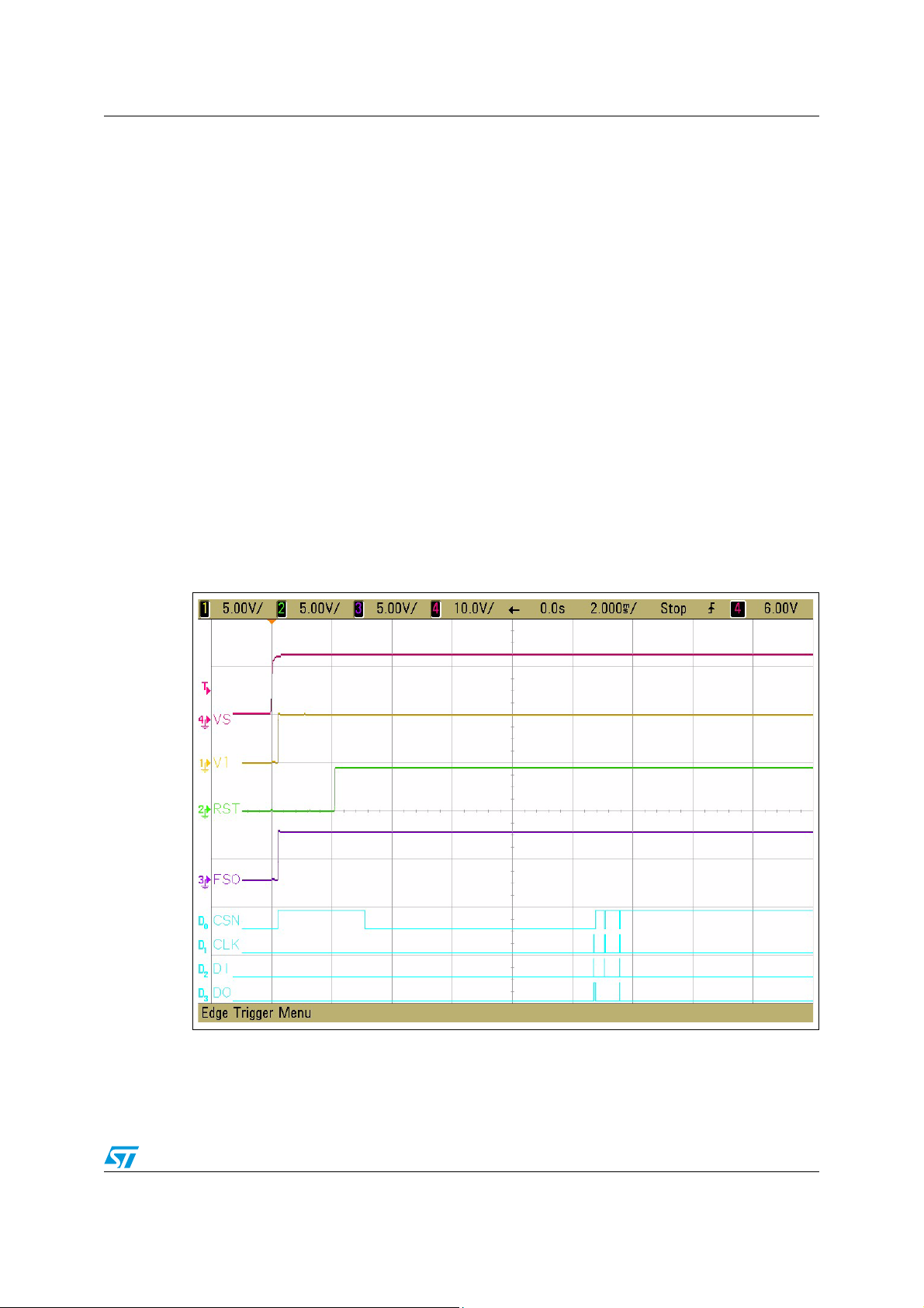
3.1 Power-on
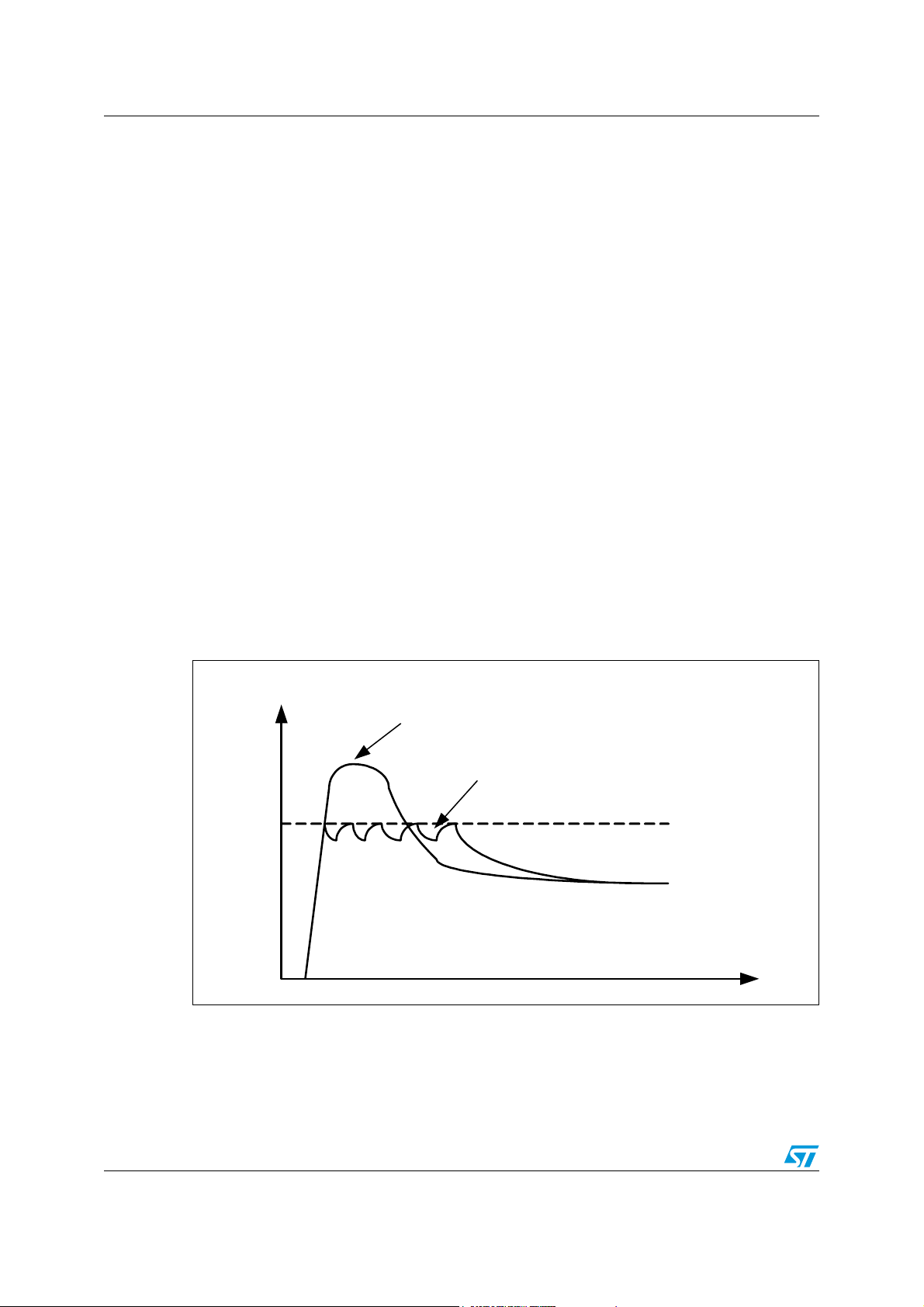
Figure 4. shows the main signal behaviour after power-on. When Vs voltage is applied, the
V1 voltage supplying the microcontroller is immediately turned On thanks to its very fast
transient response. Note that no external electrolytic capacitance is needed.
The Fail Safe Output (FSO) is switched to its inactive state - high. However the
microcontroller does not know at that time whether a power-on or a wakeup event from any
standby mode occurred. Finding the origin of the microcontroller restart is the topic of the
initialization diagnosis. Typically the microcontroller power supply - connected to the V1
voltage regulator - is switched off in power off state, Vbat_standby mode and in the case of
a hard restart after several successive fails (e.g. 7 successive watchdogs fails).
The microcontroller is restarted by NReset after a wakeup from V1 or after a watchdog fail.
During the power-on diagnosis, the root cause of the microcontroller restart should be
identified and action taken regarding the previous state. Since after NReset or V1 turn-on
the watchdog starts with Long Open Window, all this power on diagnosis has to be done
before the Long Open Window expiration (65 ms typical), otherwise the power-on diagnosis
will have to be re-started from scratch without any diagnosis on the restart reason or Cold
Start event.
Figure 4. Correct signal behaviour at power-on
15/91
Page 16
Initialization AN2751
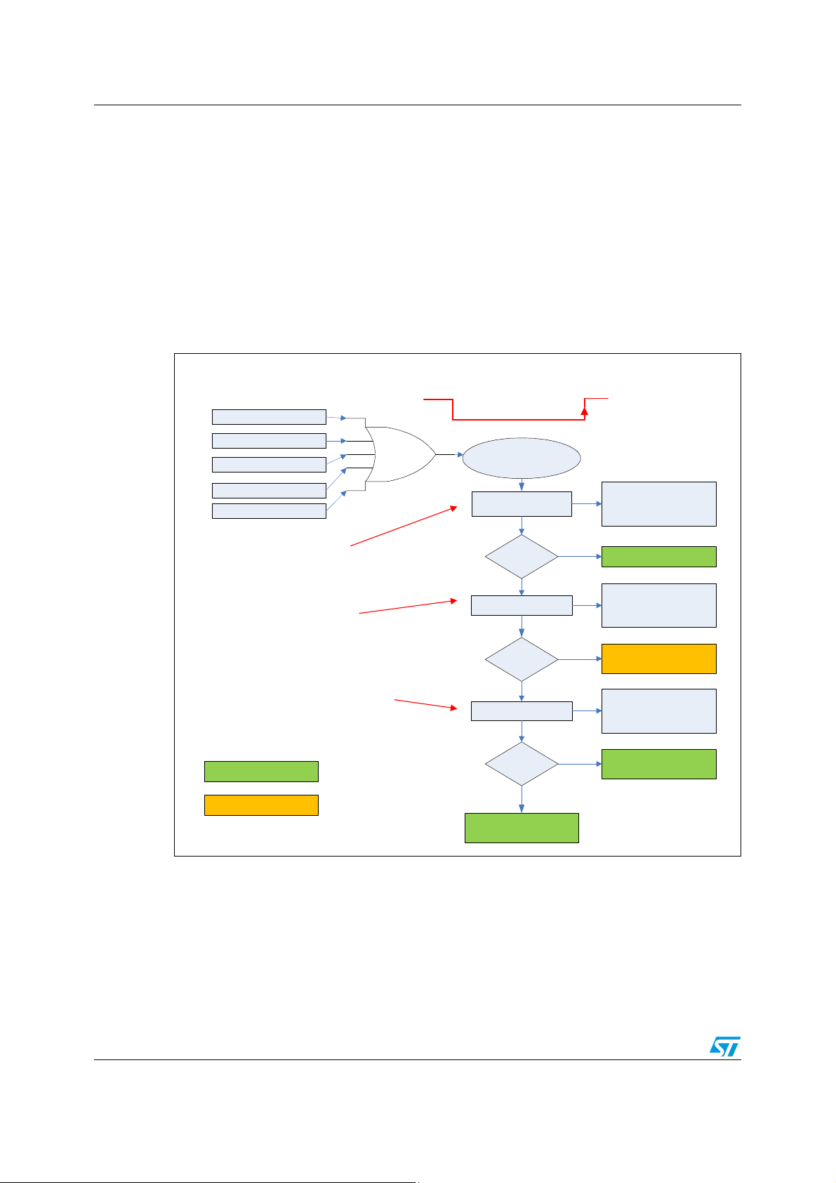
3.2 NReset generation
On an automotive system application, many external events - predictable as well as
unpredictable ones - may be at the origin of a L9952GXP NReset generation. Depending on
supply conditions, thermal conditions, voltage range stability or wakeup events, different
diagnosis and actions have to be handled by the application with the highest level of
confidence and security.
The following flowchart (Figure 5.) is a reduced overview of the NReset handling in order to
treat the possible events in the right priority order. The complete and exhaustive diagnosis
procedure is detailed in the Diagnosis chapter. In addition, the dedicated software routine
has been inserted in the appendix.
Figure 5. NReset generation and handling overview
Power ON (Cold Start)
Wachdo g Fa ilure
Vbatstby Wake-up event
V1stby Wake-up event
V1 < Vrth (for 8 us) event
OR
Nreset forc ed L ow
Nreset
Low-high transition
Power-On Detection
Nreset released
S P I In i ti a l iz a tio n
Drivers Inititialization
SR0 Access
1/ C h ec k batter y c onnec tion
2/ Check System Integrity:
- Thermal conditions
Cold Start E nte ring P ower-O n proced ure
N
Failure Detection
Y
Thermal s hutdown Detection
V1 voltage regulator Failure
Watchdog F ailure
- Su p p l y ran g e s
- Micro communication
3/ Check Outcoming Power Mode:
- Wake-up from V1 or Vbat standby
- Id en ti fy wake-up eve nt
Normal Operation
Fail-Safe Operation
Failure
N
Wake-up Detec tion
V1s tby mode
N
Mic ro Initialization be fore
Entering Active Mode
Y
Y
System Failure to be
handled at highest level
Outputs Control
Diagnosis
Wake-up source Detection
Micro Memory Content
was preserved
Entering Active Mode
After L9952GXP power-on - when Vs voltage is turned On - the first action to be performed
by the application is the Initialization Procedure.
First the status register SR0 has to be accessed in order to evaluate the cold start bit (SR0
bit 19). The SR0 should be obtained by a CR2 write. After cold start bit evaluation, the SR1
should be read for evaluation of a possible restart after any error. If thermal shutdown
neither V1 fail nor WDC Fail Counter is set, there is only wakeup from Vbat_standby mode
16/91
Page 17

AN2751 Initialization
or wakeup from V1_standby with NReset generation as possible reasons for microcontroller
restart.
At this point it is not possible to determine whether the microcontroller was restarted
because of power-on or wakeup event from any standby mode. Details regarding wakeup
from standby modes as well as explanations on the corresponding parts of flow chart will be
deeply described in the Diagnosis chapter. This chapter is aimed to give an initialization
overview only.
At the end of power-on diagnosis the watchdog has to be triggered by writing TRIG = 1. As
soon as the watchdog is triggered the Long Open Windows expires and the Window
Watchdog (WD) is started. It has then to be triggered periodically – typically every 10 ms
from the last trigger operation.
3.2.1 Power-on: cold start detection
This first step is used for checking system supply status. After power-on, when the supply
voltage Vs passes the Power-on-Reset (POR) threshold (3,8 V typical), the “cold start” bit
(SR0 bit 19) is latched. Consequently all SPI registers are initialized to their default value.
Only a power-on event latches the cold start bit - It is NOT set after waking-up from any
standby mode or after any failure occurrence (Thermal Shutdown, V1 Fail, WD Fail…).
Only the first SR0 read access immediately following a power-on returns the cold start flag.
This bit is cleared after the first complete SPI frame completion, precisely when the CSN
signal is relaxed (rising edge). A complete SPI frame means that 24 SPI_CLK pulses were
transmitted while the SPI_CSN signal was low. In the case of an SPI communication Fail, for
example, a short on the SPI_CLK signal – the cold start bit is held at 1 until the next SPI
frame completion.
3.2.2 Failure detection
Vs power supply: under/over-voltage detection
The Vs under/over voltage flags are used to point-out static problems on Vs supply – for
example, on the battery (Vbat). By default the sporadic under/over voltage events are not
saved, the L9952GXP turns the outputs in high impedance state for load protection and
automatically recovers its functionality when the under/over voltage condition has
disappeared. For safety reason, two control bits have been implemented to precisely control
the outputs behaviour in case of over/under-voltage event.
Please refer to the Diagnosis Chapter for an exhaustive description of this Diagnosis.
V
voltage regulators: failing supply detection
1,2
It may be mandatory in safety related applications, to monitor the subsystem microcontroller
RAM consistency and if needed to take corrective actions from the upper layer of the
application. The V
those coming from short to ground at start-up but also from very short under-voltage
conditions due to electromagnetic noise.
Please refer to the diagnosis chapter for an exhaustive description of this diagnosis.
V1 fail / V2 fail are flags indicating a drop of the voltage regulator output voltage below 2V
for at least 2 µs. The flags are also set after power on, if the voltage regulator output doesn’t
exceed the 2 V level within 4 ms after turn-on.
1,2
voltage regulators flags V
1fail
and V
will point-out disturbances even
2fail
17/91
Page 18

Initialization AN2751
SHT5V2 is an additional flag for V2 shortcut diagnosis. This flag is set when the output of
voltage regulator 2 doesn’t exceed the 2 V level within 4 ms after turn-on.
Watchdog failure
The watchdog has to be served during the open window, typically every 10ms after previous
refresh. As soon as the open window expires without a valid trigger, the WD fails. The WD
also fails when it is triggered too early means during the closed window. As soon as the WD
fails, the NReset signal is pulled down for 2 ms.
3.2.3 Wakeup source identification
After waking-up from V1_standby or Vbat_standby mode, an identification procedure has to
be performed to find out the wakeup source or event.
The detailed flowchart of a standard procedure can be found at Figure 28. within Standby
modes chapter. The generic microcontroller code has been included in the appendix .Those
frame has to be considered as example guidelines for a safe approach. The priority goes to
safety or error related information before considering potential wakeup sources. Depending
on your application needs and priorities this standard frame will have to be adapted.
After a transition from one operating mode to another, the current state of L9952GXP cannot
be evaluated. For this reason it is highly recommended after any wakeup event to proceed
with a full initialization of L9952GXP as shown in Figure 18.: Power-on diagnosis: detailed
flowchart.
The wakeup root cause can be identified by reading SR0 bits 13 to 18 The corresponding
bits have been set in case of a wakeup by LIN, INH or WU inputs 1-4 status change. For WU
inputs, the initial status was automatically stored before going to standby. A continuous
comparison between the initial and actual value is operated during contact sensing and the
corresponding WU input bit is set in case of a status change.
Note: The previous standby mode from which the L9952GXP was woken-up cannot be identified
after any wakeup event. In case this information is needed by your application, it has to be
saved into the microcontroller before going into the specified standby mode.
3.2.4 Microcontroller RAM integrity
This topic can be a very important issue depending on the application. In Normal conditions
the RAM content should still be valid, if the power supply voltage didn’t drop under threshold
level. Regardless the microcontroller was in halt mode and NReset was processed after
wakeup. Typical situations in which the RAM content should have been corrupted are poweron, hard restart after several successive fails and wakeup from Vbat_standby mode.
After wakeup from V1_standby mode, the RAM content should be valid. Due to the fact that
the previous standby mode cannot be detected by L9952GXP itself, it will have to be
decided – at the application level – whether the RAM content is valid or not. Some
microcontrollers integrate power on detection feature that facilitates such arbitration.
18/91
Page 19
AN2751 Initialization
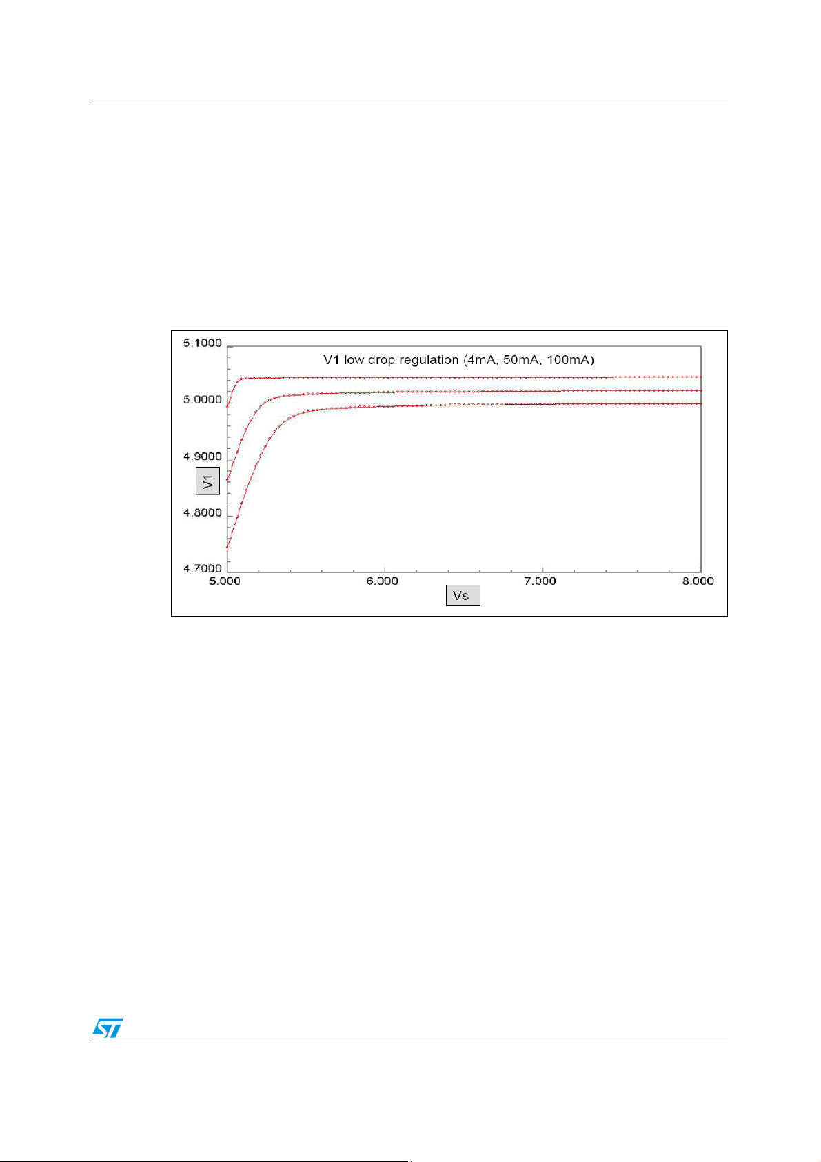
3.3 User defined initialization
Such initializations can be done anytime during run time, but in most applications it is
enough do it after start up only.
NReset level is the threshold level of V1 voltage when the NReset pin is pulled-down. This
situation can occur only during V
V1 near the limit of over current protection. The V1 regulator has low drop and the output
voltage shouldn’t fall under the NReset threshold in standard current range for Vs in
operational level. Drop of V1 voltage regulator and voltage level at output in dependence on
Vs value and V1 current is shown in Figure 6..
Figure 6. V1 voltage regulator drop
voltage around the under-voltage level and the current of
S
Vs lockout is a control bit which controls the behaviour of the high side output Out 1..4,
Out_HS of the low side relay outputs Rel1 and Rel2 and of the LIN Bus in case of Vs over/under Voltage conditions. When V
lockout bit is set the outputs are automatically disabled-
S
means turned-off to their default value when an over/under voltage condition is detected.
The outputs remain off also when the over/under voltage condition disappears. The over/under-voltage Status Bits (SR1, D0/D1) have to be cleared in order to turn-on the outputs.
If the Vs lockout bit is not set (default configuration), the outputs are automatically turned On
when the over-/under-voltage condition disappears.
19/91
Page 20
Watchdog operation AN2751
4 Watchdog operation
4.1 Initialization - Long Open Window (LOWi)
After some specific events, the L9952GXP’s window watchdog counter will start to operate
with a Long Open Window (LOWi) - typically 65 ms.
The events at the origin of a LOWi are the following:
● “ Cold ” NReset after power-on.
● “ Warm ” NReset under Vs supply.
● “ Wakeup ” from Vbat_standby or from V1_standby modes.
● “ Watchdog Failure ”.
● “ V1 Voltage regulator current increased above the threshold current in V1_standby
mode-e.g. Iv1 > Icmp_rise.
The Long Open Window (LOWi) allows the microcontroller to run its own setup through its
boot sequence or to recover its normal activity after a “low-power” or “Halt” period before
triggering the watchdog via the SPI interface.
During this time slot the watchdog has to be triggered indifferently between the beginning
and the end of the Long Open Window.
Figure 7. describes the WD behaviour in case the LOWi expires without a valid trigger. In
this case, an active low reset pulse is generated on the NReset output and another LOWi is
started. After eight consecutive watchdog failures the V1 is turn-off for 200 ms. After this
delay another LOWi is started. If watchdog is still not triggered after seven further
consecutive reset procedures, the V1 regulator is completely turned-off and the L9952GXP
device goes into Vbat_standby mode until next the wakeup event occurrence (e.g. via LIN,
CAN/INH).
When the watchdog is triggered before the LOWi expiration the initialization procedure is
over. The microcontroller will then have to trigger the watchdog within the standard periodic
open windows (typically every 10 ms).
Figure 7. Power-on behaviour: LOWi failed
Long Open
Window
Reset
V1 turn off
for 200ms
Forced V
Standby
bat
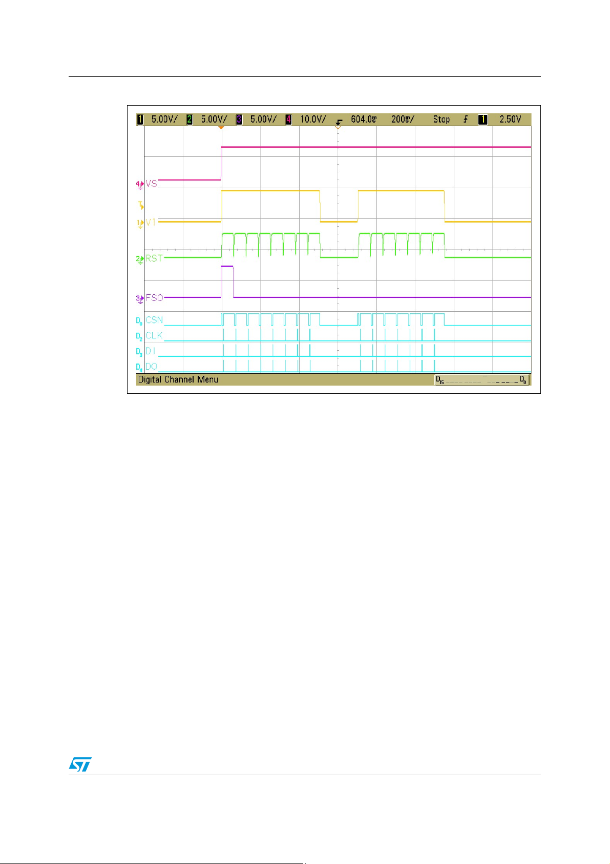
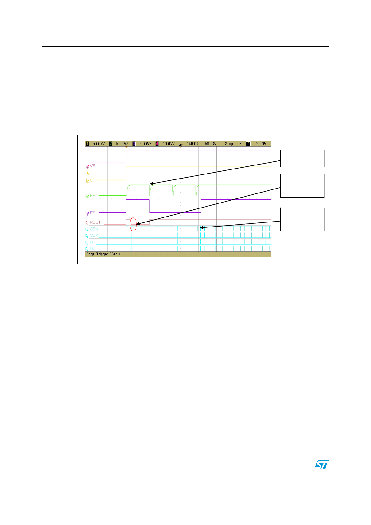
Screenshots of the signals behaviour after a power-on with continuous watchdog failures
are shown in Figure 8.. As the watchdog was not triggered 15 consecutives times, V1 was
switched-off and the device forced to Vbat_standby mode. After the first Long Open Window
failure, the Fail Safe Output (FSO) is turned to active (low) state. This output remains active
till the next successful watchdog trigger. If the device is switched to force Vbat_standby
mode, after wakeup the FSO output is for the first Long Open Window in not active state
again until the new watchdog failure occurs (see Figure 8.).
20/91
Page 21
AN2751 Watchdog operation
Figure 8. Power-on procedure without watchdog trigger
4.2 Normal operation - window watchdog
The window watchdog procedure enables periodic control of the microcontroller during
normal Operation (Active mode). Any unexpected deviation of the quartz period (even too
slow or too fast) may lead to dysfunctions and have dramatic consequences in some
security related applications. Thanks to the Watchdog Trigger procedure, both sustainability
and correctness of the microcontroller’s frequency are permanently checked.
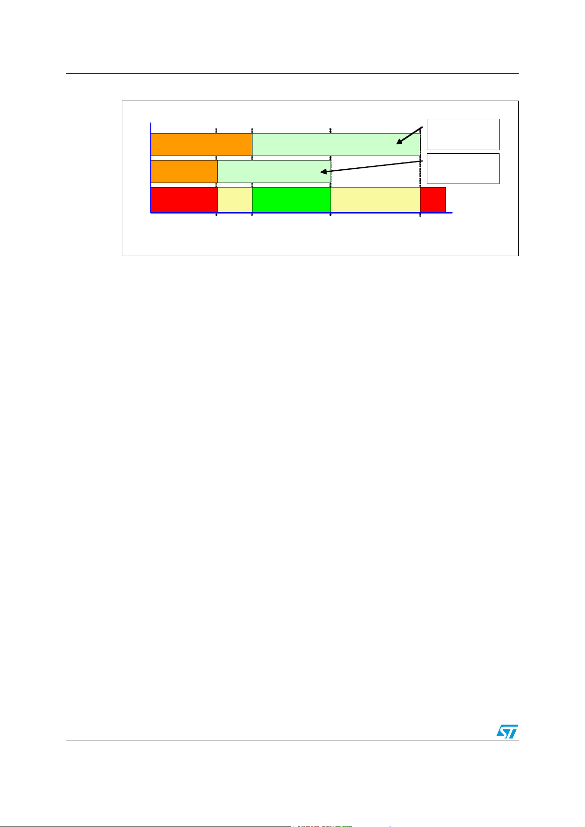
Figure 9. shows the different watchdog trigger behaviours we can obtain depending on the
different corner conditions. A correct watchdog trigger starts the window watchdog with a
closed window (from 4.8 ms min. to 7.2 ms max.) followed by an open window (from 8 ms
min. to 12 ms max.). The micro has to serve periodically the watchdog by alternating the
trigger bit TRIG (CR0-D19) during the open window. A correct watchdog trigger signal will
immediately starts the next closed window.
21/91
Page 22
Watchdog operation AN2751
Figure 9. Windows watchdog and trigger timing areas
Closed Window
Tmax
Closed Window
Tmin
Watchdog
Fail
4.8 7.2 12.8 19.20
Unde-
fined
Open Window
Tmin
Safe Trigger
Area
Open Window
Tmax
Undefi ned Fail
Max. Spe cified
Timings
Min. S pecifie d
Timings
Time
[ms]
Note: The silicon parameters and the corner conditions have a strong impact on the Windows
Timings. To avoid any potential Watchdog Failures at extreme conditions, it is highly
recommended to trigger the Watchdog in the middle of the Safe Trigger Area - means
at 10ms. A WD trigger during the undefined area could either be detected as correct or a
failing Trigger. WD triggering during a closed windows will causes an “Early write” trigger
failure. In this case the L9952GXP resets the microcontroller - means NReset Pin is pulled
low for 2 ms.
Naturally, it is possible to perform at any time a CR0 write access, but the microcontroller
has to make sure that the TRIG bit Polarity (CR0-D19) remains unchanged outside the safe
trigger area otherwise an “Early write” trigger failure may occur.
4.3 Watchdog fail
The watchdog (WD) has to be served during the open window, typically every 10 ms after
previous refresh. As soon as the open window expires without a valid trigger, the WD fails.
The WD also fails when it is triggered too early means during the closed window. As soon as
the WD fails, the NReset signal is pulled down for 2 ms. All outputs are switched off, the
FSO output is forced active (low) and the watchdog counter (WDC) (SR1 bits 12 to 15) is
incremented e.g. set to 1. After 2 ms, NReset is released to inactive (high) state and the
Long Open Window (LOWi) starts.
Note that after waking-up from any standby modes, and during the complete LOWi, the
outputs recover the same value as before entering the standby mode. Important is that all
outputs are switched off in case of WD failure.
Before the first LOWi expiration, the WD has to be triggered. If the WD is triggered
successfully, FSO is switched to inactive (high) and all outputs are configured to their
defined values (written in CR0 together with the WD trigger command).
If the WD trigger fails again during LOWi, e.g. LOWi expires without triggering, the NReset is
processed again and the WDC is incremented. After 8 successive LOWi without watchdog
triggering, the V1 is switched off. After 200 ms V1 is switched on again and 7 additional
LOWi are issued. If the WDC reaches 15, L9952GXP is forced to Vbat_standby mode and
the WDC is cleared. WDC is also cleared after any valid watchdog trigger. Therefore, if your
application wants to monitor the number of successive watchdog failures, the WDC status
(SR1 bits 12 to 15) has to be read after any reset event and before watchdog triggering
22/91
Page 23

AN2751 Outputs control
5 Outputs control
5.1 Outputs descriptions
The L9952GXP provides a complete set of outputs for driving different kinds of loads:
● Two 5V low-drop voltage regulators (250 mA and 100 mA continuous mode)
● Five high-side driver outputs for driving LEDs, Bulbs or Hall Sensors
● Two low-side driver outputs for driving relays
● Two digital outputs for driving microcontroller digital inputs
After Vs power-on, CR0, CR1 and CR2 registers are at default value 0x000000. This means
that all outputs are switched Off.
Note: Important : Outputs behaviour after a failing watchdog
After a first WD failure, all L9952GXP outputs are turned Off. They cannot be turned on
(even during LOWi) until the watchdog is served correctly. As the HS output control bits
remain unchanged, the HS outputs will enter the configured state automatically if the
watchdog is triggered correctly or after waking-up from forced Vbat_standby mode.
5.1.1 Voltage regulator V1
The V1 voltage regulator is the core functionality of the L9952GXP and particular efforts
have been spent both for improving the performance and for optimizing the complete system
area.
As a result the L9952GXP offers strong differentiating features for serving your application
needs:
● Very low quiescent current
● Optimized transient response
● No electrolytic output capacitor need
● Continuous I
● Advanced protections against overload, over-temperature, short circuit, reverse biasing
current monitoring functionality
CMP
Exhaustive information on V1 voltage regulator is available in Diagnosis and Standby modes
chapters. Additionally an information summary in Appendix B covers some specific
scenarios regarding V1fail and I
monitoring topics.
CMP
Note: The V1 voltage regulator is also used for supplying internal logic circuitry and digital outputs
of the L9952GXP (Dig_out3, Dig_out4 and FSO). As a consequence I
is the sum of the
CMP
V1 external current plus the internal logic circuitry and Digital outputs currents.
5.1.2 Voltage regulator V2
Voltage regulator 2 has 4 different operating modes:
● Always Off in all power modes
● Always On in all power modes
● On in run mode only and Off in standby modes
● On in active mode and V1_standby mode; Off in Vbat_standby mode
23/91
Page 24
Outputs control AN2751
After voltage regulator V2 has been turned On, the SHT5V2 flag (SR0 bit 12) should be
checked to get a status of the regulator output and connected load condition. Details about
this flag can be found in diagnosis chapter.
5.1.3 High-side drivers
Any of the five High-side outputs can be configured to one of the following modes by setting
the corresponding combination of bits in the CR0:
● Off – in this mode the output is switched Off in all operating modes.
● On – in this mode the output is switched On in Active mode and it is switched Off in
V1_standby and Vbat_standby modes.
● PWM 1 or PWM 2 – in these modes the output signal is controlled by the signal on the
PWM1 or PWM2 input in Active mode. In V1_standby or Vbat_standby mode the
output is switched off.
● Timer 1 or Timer 2 – in these modes the output is periodically switched on and off
according to the setting of the selected timer. Typically this mode is used to periodically
supply the external contacts, synchronized with the cyclic monitoring of the wakeup
inputs. This configuration is possible in all operating modes.
Additionally, on HS Out1 to HS Out4 the open load threshold levels can be configured to
2 mA or 8 mA (CR0-D0…D4).
For Out_HS an auto recovery feature is available in active mode (see Figure 10.). This
enables driving loads with an initial current higher than the over current limit (e. g. inrush
current of cold light bulbs). If the Auto-recovery O_HS_REC bit is set (CR2-D5), Out_HS will
automatically be restarted after any over-current shutdown event.
Figure 10. Out_HS current limitation in auto recovery mode
Curren t
Limitation
Load
Current
Unlimit ed
Inru s h Cu rrent
Limited Inrush Current in
programmable Recovery
Mode
t
24/91
Page 25

AN2751 Outputs control
5.1.4 Low-side drivers
Two low-side driver outputs Rel1 and Rel2 are available for driving external relays – e.g. for
power window control. These outputs can be switched on and off by setting the
corresponding bits in the CR0.
The Rel1 and Rel2 output control bits are cleared by default after a first watchdog failure
occurrence. Refer to the chapter “Driver Control after power-on” for detailed information.
5.1.5 Digital outputs
In both Active and V1_standby modes, the Outputs Dig_out3 and Dig_out4/INT offer the
possibility to transmit real time signals from the operating side to the processing side of the
application without waiting for a periodical SPI access. Three different configurations are
possible:
● Direct looping of WU inputs when status changes.
● Direct looping of High-side open-loads when status changes.
● Interrupt generation when waking-up from V1_standby mode.
A significant advantage of direct looping is the possibility to transmit signals coming from the
WU inputs pins - at Vs voltage level to the digital output pins - at TTL voltage level e.g. 5V.
The direct looping of open-load status from High-Side outputs was specifically implemented
to connect Hall sensors outputs requiring high real time processing speed. For this purpose
the open-load threshold current is configurable on HS Drivers 1 to 4 between 2mA and 8mA
(CR2 -bits 0 to 3).
Additionally, the Dig_out4/INT output can be configured (CR1 bit 20) to generate an interrupt
signal to the microcontroller (2ms active high pulse) in case of a wakeup from V1_standby
mode through WU inputs, LIN, INH, SPI, HS open-load and I
is set to 1 (CR1 bit 20) the looping Option on Dig_out4 is disabled and the NRESET
generation is disabled. This specifically addresses applications where the microcontroller
must preserve its memory content and have a fast wakeup and fast recovery after an
interrupt generation.
All factors influencing the information at the digital outputs are detailed in the digital output
chapter.
5.2 Outputs control after power-on
All L9952GXP outputs can be switched-on after power-on as soon as the NReset signal has
been released untill expiration of the LOWi.
For CR0 write access, the TRIG bit has to be considered with special care. After power-on
(means Cold-Start bit is set) the trigger bit polarity has to be set to “1”.
If the outputs are turned On, and watchdog is not triggered, they stay On until the long open
window expires. Then the outputs are automatically disabled (turned Off and blocked until a
correct watchdog trigger or a wakeup from forced Vbat_standby mode occurs); HS Control
Bits in CR0 remain unchanged; LS control bits in CR0 are set to 0) and FSO is turned to
active (low) state. After NReset generation, outputs stay off until first successful watchdog
trigger. However, every correct watchdog trigger defines the value of all output
configurations. So when the watchdog is triggered the outputs are set to configuration that
was sent to the L9952GXP during this watchdog trigger procedure (Trigger bit and output
v1
> I
CMP_ris
. When INT_enable
25/91
Page 26
Outputs control AN2751
control bits are both located in CR0). On the next screenshot is caught behaviour when
REL1 output was turned On after power on. But the watchdog was not triggered and long
open window fails 3 times. Than the watchdog was triggered correctly by CR0 with a default
value where all outputs are turned off.
Note: In case of V1_standby mode wakeup event (LIN, INH), the trigger bit was not reset to ‘0’ by
NReset event. The previous trigger bit polarity should have been stored by the
microcontroller in order to correctly invert it after waking-up. otherwise the WD is triggered
with a wrong Trigger bit and the LOWi is closed with a Watchdog failure.
Figure 11. LS output behaviour at failing watchdog
LOW Fail
Rel1 output
turn ON
Watchdog
triggered
Refer also to Figure 12. and observe the REL1 behaviour in a different scenario.
5.3 Fail Safe Output (FSO)
The fail safe output is a standard automotive safety functionality implemented for reporting
abnormal behaviour of any power management system IC.
In the case of an active FSO signal, external Safety Logic or an additional microcontroller
will take-over the control of the security related Drivers so that system sustainability is
assured.
The following four events force the FSO output signal to active low state:
● Entering Vbat_standby mode
● Watchdog failure
● V1 under-voltage
● Second thermal shutdown level - TSD2
The next screenshot illustrates a situation where the LOWi fails 15 times after power-on and
the device is switched to force Vbat_standby mode. First after power-on, the FSO output
remains in its inactive state - high until expiration of the first LOWi. As the watchdog has not
been triggered during the LOWi, the device detects a watchdog failure and the FSO signal is
26/91
Page 27
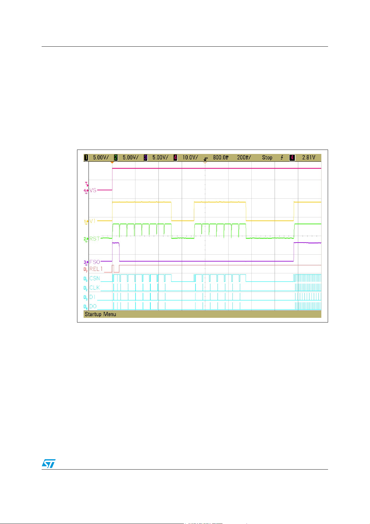
AN2751 Outputs control
forced to its low active state. The FSO signal remains active until the Watchdog is correctly
triggered.
In case the watchdog is correctly triggered before the first LOWi expiration, the FSO stay in
inactive state and the L9952GXP outputs are set to the user-defined state, transmitted
through the watchdog trigger SPI frame (same write access on CR0 control register).
Note that after wakeup, the LS Output remains Off due to the previous watchdog failure.
The Rel1 output is turned Off at the first watchdog failure and stays off even after a wakeup
from forced Vbat_standby mode because the REL1 and REL2 control bits have been
cleared after the watchdog failure.
Figure 12. FSO behaviour after LOWi failure, forced Vbat_standby and wakeup event
Refer also to Figure 11. and observe the FSO behaviour in a different scenario.
Note: Outputs behaviour during active FSO.
As soon as FSO enters its active low state, all L9952GXP outputs are turned Off. They
cannot be turned On (even during LOWi) until the FSO is released – e.g. the watchdog is
served correctly. As the HS output control bits remain unchanged, the HS outputs will enter
the configured state automatically if the watchdog is triggered correctly or after waking-up
from forced Vbat_standby mode. Due to the fact that the trigger bit is within the same
register than the Outputs configurations bits, you should take care to overwrite the output
configuration with the correct values each time you will invert the trigger bit (for example by
applying a software mask).
27/91
Page 28

Wakeup inputs AN2751
6 Wakeup inputs
Several settings can be applied on the WU input Pins in order to configure the contact sense
to perfectly match with your application requirements. The following two major settings have
to be considered:
● The cyclic contact sense supported by both stand-by modes.
● The static contact sense mostly adapted for waking-up from Vbat_standby mode – e.g.
for applications where the microcontroller can be completely stopped and where the
current consumption has to be drastically minimized.
6.1 Cyclic contact sense
Both standby modes support the cyclic sense of the contacts. The main advantage of the
cyclic contact supply and sense is a significant reduction in power consumption. For the
open active contact (closed in not active state) the power consumption in static mode is
approx 10mA for one contact. With the cyclic contact sense, this contact supply current is
reduced only to a short time when the contact is checked while the current consumption of
the L9952GXP increases by approximately 65uA. Contact sense is done during “On Time”
of the timer selected for cyclic sense functionality. During the remaining timer period the
contact is not powered and not consuming any power. Of course this feature has an effect
for some contact configurations like opening contact, contact which have two stable
positions (On/Off) and contacts with a parallel or a parasitic resistive load (e.g. humidity).
However, regardless of the configuration, the cyclic monitoring limits the current
consumption in case of a stuck contact switch.
To reduce power consumption in the timer Off-time, the proper configuration of each input
for current sink or current source has to be done (CR1). The current sink or current source
configuration is active only in timer Off Time for cyclic sense to reduce WU input leakage
current when the contact is not powered and floating. In time when the contact is checked
(timer On Time), the WU input is automatically reconfigured to the setup used in Active
mode where an internal pull down of 200 KΩ is activated.
For leakage current limitation, the current source configuration is recommended for
active low contacts and the current sink configuration is recommended for active
high contacts.
28/91
Page 29

AN2751 Wakeup inputs
Figure 13. Cyclic contact sense: contact connection
Cyclic Contact Supply
Cyclic Contact Supply
with Timer 2 typica lly
with Timer 2 typica lly
OUT1 … OUT4
OUT1 … OUT4
OUT_HS
OUT_HS
C ontact high active
WU1 … WU4
WU1 … WU4
L9952
L9952
C ontact high active
Contact low active
Contact low active
To use the cyclic sense the contact has to be powered by any HS driver (Out1-4 or Out_HS).
According to the description in the chapter “prepare for standby”, the output has to be set to
Timer 1 or Timer 2 mode to be able to power the contact in standby mode. The timer 2 is
intended for contact sense, but timer 1 can be used as well if the timer 1 settings are
appropriate. The cyclic sense of the contact is based on the selected timer settings. The WU
input which is used for contact sense must have the filter configuration corresponding to the
used timer settings (period and On-time).
Figure 14. Cyclic contacts sense: wakeup events
50ms
Ti m er 2
100µs resp . 1ms
Input con fig
Control Register 1
Stat e
Status Bit
Suppl y
WUx
V
WUy
V
D19
Wake Up Input
high active
Wake Up Input
low active
Wake Up Input
active
low high
80µs re sp. 800µs
Input config
Control Register 2
D10 - D17
Contact
WU I n pu t
Contac t
Active Mode
16us Filter
low
t
Wake Up
Event
29/91
Page 30

Wakeup inputs AN2751
In case of improper configuration of the HS output and the WU input filter, the wakeup
functionality from standby mode is not working or a transition to standby mode is not
possible, because of immediate wakeup.
If the configuration is correct and the device is switched to standby mode, during every timer
ON time of the selected timer, the contact supply is activated and the contact status is
evaluated at the WU input. The input signal is filtered (80us blanking, followed by 16us
filtering in typical conditions) and the wakeup is processed in case that a level change on the
input is detected compared to the previous qualified value.
6.2 Static contact sense
In static contact sense configuration, the contact has to be powered by an external power
source (see Figure 15.).
Figure 15. Static contact sense
Constant Contact S upply
V
V
S
S
WU1 … WU 4
Contact high active
C onta c t low ac tiv e
L9952
The big advantage of this mode is the extremely low power consumption of the L9952GXP
(typically 7 µA). If only closing high active or low active contacts are used, the complete
power consumption of the contact sense is lower than for cyclic sense. To achieve the low
power consumption, proper configuration of current sink or current source at the wakeup
inputs has to be set for each WU input. For leakage current limitation, current source
configuration is recommended for active low contacts and current sink configuration
is recommended for active high contacts.
For this mode the static filter has to be selected on each dedicated WU input. If the static
filter is configured, the input is monitored with a 64us filter typical. If any status change is
detected at the input, the L9952GXP enters the wakeup procedure and the value is stored in
SR0 bits 13 (WU1) to 16 (WU4). Details of the system wakeup by static contact sense are
shown in the next figures. The first diagram shows the signals for active High contacts and
the second diagram for active low contacts.
During static contact sense, it is also possible like for cyclic contact sense to use the WU
inputs with a configured filter synchronized with Timer 1 or with Timer 2. The contact value
will be evaluated correctly, but only during timer ON time. The wakeup functionality will also
works, but the L9952GXP core current consumption is increased as in cyclic mode.
30/91
Page 31

AN2751 Wakeup inputs
Figure 16. Static wakeup by active-high contacts
No Wake Up
Event
t < 64µs
t = 64µs
t > 64µs
Wake Up
Event
t = 64µs
t
0.55 * V
at WUx
Inpu t Volt age
S
Wake Up
Request
enh. Iq
1V
WU Input
St at u s B it
Wake-up requests starts oscillator and other internal circuitry increas ed Iq
Figure 17. Static wakeup by active-low contacts
VS - 2V
0.45 * V
Wake Up
Request
S
at WUx
In pu t V o l t a ge
WU Inpu t
Status Bit
Wake-up requests starts oscillator and other internal circuitry increase d Iq
No Wake Up
t < 64µs
Event
t = 64µs
t > 64µs
Wake Up
Event
highlow low
t
t = 64µs
t
lowhigh high
t
31/91
Page 32

Diagnosis AN2751
7 Diagnosis
L9952GXP provides a wide range of diagnostics information through the SR0 and SR1
status registers. These diagnostic flags are related to output drivers, junction temperature,
voltage supply monitoring, and wakeup inputs.
The first diagnostic to be performed is the initialization diagnosis. But several additional have
to be periodically monitored to check the status of the application and take corrective action
if needed. These diagnostic flags are related to:
● Output diagnosis (open-load / over current)
● Chip junction temperature (TW, TSD1 and TSD2)
● Vs monitoring (Over-voltage / Under-voltage)
● V1 monitoring (short circuit, number of restarts after TSD2 and voltage glitch)
● V2 monitoring (short circuit and voltage glitch)
● Wakeup input sources (CAN, LIN, WU Contacts, OL Contacts and SPI)
● Watchdog trigger and successive watchdog failures.
7.1 Initialization diagnosis
The following flowchart (Figure 16.) describes in details the recommended initialization
procedure. Additionally the dedicated Software routine has been inserted in the appendix.
At power-on, when Vs voltage is applied, the V1 voltage supplying the microcontroller is
immediately turned on thanks to its very fast transient response and the NReset signal is
generated. Note that no external electrolytic capacitance is needed.
At that time, the microcontroller does not know whether a power-on or a wakeup event from
any standby mode occurred. Finding the origin of microcontroller restart is the topic of this
initialization diagnosis. Typically microcontroller power supply - connected to V1 voltage
regulator - is switch off in power off state, Vbat_standby mode and in the case of a hard
restart after several successive fails (e.g. 7 successive watchdog fails).
The microcontroller is restarted by NReset generation after a wakeup from V1 or after a
watchdog fail. During the power-on diagnosis the right reason of the microcontroller restart
should be identified and action taken regarding the previous state. Since after NReset
generation or V1 turn-on the watchdog start with long open window, all this power-on
diagnosis has to be done before the long open window expiration (65ms typical), otherwise
the power-on diagnosis will have to re-started form scratch without any diagnosis on the
restart reason or Cold Start event.
32/91
Page 33

AN2751 Diagnosis
Figure 18. Power-on diagnosis: detailed flowchart
Read SR0 by
write to CR 2
SR0. D19
SR1. D4
SR1. D5
SR 1. D 12-15
Ide nti fy wa ke -u p s ou rce
SR 0. D13-16
SR0. D0-3
- Conf. contacts s tatic sense
- Read Status Register 0
SR 0. D13-16
Nreset
L ow -h ig h tra ns itio n
Initializ e
SPI peripheral of uC
SW SPI Drivers Init
Read Status Register 0
Cold Start
= 1
N
Read Status Register 1
TSD2
= 1
N
V1 fail
= 1
N
WD fail
? 0
N
Wakeup from any standby mode
(except wake -up from V1stby by LIN, CAN (INH), SP I or Iv1>Icmp)
Check uC
power on *
N
Soft Initializ ation
Wux ?
stored value
N
HS_OL ?
stored value
N
Wux ?
stored value
N
Unknown reason
For wake-up
Nreset releas ed
Y
Power ON Reset procedure
(Initialization)
- Checking for restart because of any fail
Y
Y
Y
Y
Y
Y
Y
- RA M validity is not possible to evalua te from these information
V1 < 2V
for t > 2us
Wa tchog trig ge r pro blem
(e.g. timing o r sync hronizatio n)
If WD fail = 1 … un-catch wakeup
(e.g. ICM P wake up)
* if feature is supported by uC
- Wakeup from V1 standby mode (no fail)
- RA M content should be valid
Wakeup by contact
ac tivity
Wakeup by open
load change
Wakeup by contac t
ac tivity
- Wakeup from not know reas on e.g. EMI
- Trigg er watc hdog
- Reinitialize CRs and go standby again
- L9952 registers were set to default
- R AM c onte nt is not va lid
SR1. D9-11
V1 short/overload
SR0. D18
SR0. D17
SR 0. D13-16
SR0. D0-3
5V R estarts
= 0 ?
TSD2 after
Note:
If WD fa il = 8, a „G o_V
and ICM P = 1 causes V
defaut HW
default HW
Unknown reason
For wake-up
Y
N
- Wakeup from Vbat standby mode (no fail)
- Mirro r of regi sters inside uC were c leared
- RA M content is not valid
LIN
IN H
= 1
N
Wux ?
value
N
HS_OL ?
value
N
Y
= 1
N
Y
Y
Y
Vbatstby after
8x TSD 2
witho ut watc hdo g trigg er
1
to s witch o ff perman ently
1
Wakeup by
LIN
Wakeup by
CAN
Wakeup by contact
ac tivity
Wakeup by open
load ch ange
co mpl ete the L995 2
Initializ ation
33/91
Page 34

Diagnosis AN2751
7.1.1 Cold start diagnosis
After power-on, when the Supply Voltage Vs passes the Power-On-Reset (POR) threshold
(3,8 V typical), the “cold start” bit (CR0 bit 19) is latched (see Figure 19.). Consequently all
SPI registers are initialized to their default value. Only a power-on event latches the cold
start bit - It is NOT set after waking-up from any standby mode or after any failure
occurrence (Thermal Shutdown, V1 Fail, WD Fail…).
Only the first SR0 read access immediately following a power-on will return the cold start
flag. This bit is cleared after the first complete SPI frame completion, precisely when the
CSN signal is relaxed (rising edge). A complete SPI frame means that 24 SPI_CLK pulses
were transmitted while SPI_CSN signal was low. In case of an SPI communication Fail –
e.g. a short on SPI_CLK signal – the cold start bit is hold at 1 until the next SPI frame
completion.
Note: If your application needs to monitor the cold start information or identify the wakeup event
source, a SR0 read access has to be performed immediately after any power-on or NReset
events. It is recommended to choose a CR2 write access rather than a CR0 write access for
reading the SR0 content:
●
In case of a wakeup from V1 or Vbat_standby mode, a CR0 write access overwrites the
predefined Trigger as well as the V2 and the outputs configurations whereas a CR2
write access has a smaller influence at application level and by the way is a safest
procedure depending on the targeted application.
●
Naturally and depending on the targeted application, it is also possible to configure the
outputs directly after an NReset generation.
7.1.2 Vs power supply: under/over-voltage detection
Vs under/over-voltage diagnosis flags can be monitored after power-on and then
periodically during active mode. Two Status flags are available:
● The under-voltage flag UV (SR1 bit 1) signals that Vs dropped below the under-voltage
threshold (Vsuv) e.g. 5.5V typical.
● The over-voltage flag OV (SR1 bit 0) signals that Vs reached the over voltage threshold
(Vsov) e.g. 20V typical.
After any under/over voltage event, all HS, LS and LIN outputs (OUTx, RELx, LIN) are
switched to high impedance state by default (load protection). If the under/over-voltage
condition disappears, an automatic recovery feature (active by default), makes all outputs
recover their previous state (according to CR0 settings).
Additionally, for security concern, two control bits have been implemented:
● The automatic recovery feature can be disabled with the V
this
bit is set, all outputs will remain off even after over/under-voltage recovery condition
S LOCK Out
has disappeared, until the status bits SR1 bit 0 and SR1 bit 1 are cleared by a CLR
control command (CR1-21).
● The LS_
bit (CR2 bit 19) enables to control separately the low-side outputs
OVUV
behaviour (REL1, REL2) in case of under/over-voltage.
Note: 1 If the under-voltage bit is latched but not the cold start one, then the Vs voltage is in the
range of 3.8V to 5.1V. In that particular case, the L9952GXP configuration remains valid: Its
internal SPI registers are not reset and its outputs drivers remain unchanged.
2 V1 and V2 voltage regulators remain on after a Vs over-voltage.
bit (CR2 bit 4). If
34/91
Page 35

AN2751 Diagnosis
7.1.3 V
voltage regulators - failing supply detection
1,2
Depending on the application, it could be mandatory, at the upper application layer, to
monitor the subsystem microcontroller RAM consistency and if needed to take corrective
actions. The V
(SR0 bit 5) and V
1fail
(ST1 bit 6) flags are dedicated for this purpose. The
2fail
Figure 19. illustrates V1 or V2 voltage regulator behaviour under specific conditions.
The following two scenarios have to be considered:
At initial turn-on of V
If a short to ground is detected (V
voltage regulators
1,2
< 2V) for at least 4ms then the V
1,2
respectively V
1fail
2fail
flag is latched (SR1 - bits 5/6) and dedicated regulator is switched-off to avoid thermal
cycling at static short circuit.
In case of a V
event the L9952GXP automatically enters Vbat_standby mode and all its
1fail
outputs are turned Off. The re-activation or wakeup of the device can be achieved with
signals from the CAN, LIN, WU
or SPI. The current leakage origin can then be found by
1..4
reading the SR0 and SR1 status registers.
In case of a V
event the voltage regulator is purely switched-off. Additionally the SHT5V2
2fail
flag is latched (SR0 bit 12) to indicate a V2 short. A clear command is required to re-activate
V2 (CR0 bits 17/18).
During active mode
In case of V
(SR0 - bit 5 for V
electromagnetic disturbances. When the V
microcontroller RAM consistency cannot be guarantied anymore and the upper application
layer has to take the adequate corrective action.
voltage regulator drop below 2V for at least 2 µs, the V
1,2
and bit 6 for V
1fail
). These under-voltage events are typically due to
2fail
1fail
or V
have been latched, the
2fail
bits are latched
1,2 fail
Note that the V
1fail
and V
CLR bit (CR1 bit 21) before re-activating the voltage regulators.
Note also that during active mode, if the voltage drop is below V
the NReset is immediately forced to low. This is one of the root events that can trigger the
NReset generation. The other events will be developed within the next chapter.
7.1.4 NReset generation
As we have seen any short disturbance on the supply lines can affect the Memory content of
the microcontroller and bring the application out of control.
This is why an NReset signal will be generated as soon as the disturbance on the supply
lines will reach the specified range and as soon as it will remain during the minimum
specified period. The following figure illustrates this behaviour.
failing bits have first to be cleared by a SPI write access on
2fail
for at least 8µs (typical)
rth
35/91
Page 36

Diagnosis AN2751
Figure 19. Voltage thresholds and NReset generation
Vs[ V ]
V
1/2
NRes et
V
SUV
V
POR
[ V ]
V
RT1/2
V
1FA IL
High
Low
12
5.5
5
Cold Start Bit is set
>4m s
V1 short detected
Vbatt standby
100us
t
WDR
Power-on-Reset
thres ho ld
t < t
FT
No Res et
generated
L9952GXP S pecification P arameters
tFT: V1 undervoltage F ilter Time
: R ese t Re acti on Ti me
t
RR
: Watchdog ResetP ulse Time
t
WDR
Control Registers are set
to default values
t > t
FT
t
t
RR
2us
V
FailFlag
1/2
is set
WDR
Vs Undervoltage Bit
ist set
t > t
FT
t
RR
7.2 Output drivers diagnosis
Open load flags are available for HS outputs Out1-4 and Out HS. These flags are set
immediately when an open-load condition is detected during output switch-on and cleared
immediately when the open-load condition disappears and the corresponding output is
switched on. If an output is configured to timer mode, the open-load is detected during ON
time only. So the flag is set and cleared periodically according to the timer settings. The
same behaviour will be observed if an output is configured for PWM mode: The open-load
flag is set only during ON time of the output.
Over current flags are latched when an over current is detected on Out1-4, Out_HS or
Rel1-2. The output where the over current is detected is immediately switched off and stays
off, until the status flags are cleared by setting the CLR bit of CR1-21.
Additionally the Out_HS behaviour is configurable after an over-current event. By default,
the auto-recovery bit O_HS_REC (CR2 bit 5) is disabled and the output is switched off. If
auto recovery is enabled, the output is restarted automatically after an output over-current
shutdown. The auto recovery filter time is 400xTosc.
36/91
Page 37

AN2751 Diagnosis
CSN h
igh
dCL
K
f
d
b
it0(faul
d
ition) i
D
O
(
f
7.3 Junction temperature diagnosis
Temperature control is a protection feature to avoid thermal destruction of the device. If the
chip junction temperature exceeds 130°C, the temperature warning TW bit is set in SR1.2.
Additional increasing of the junction temperature over 140°C sets the Thermal Shutdown 1
bit and all outputs are switched off, except the V1 which remains ON. If the temperature
increases over 155°C the Thermal Shutdown 2 bit is set and V1 is switched off for 1s. After
1s the V1 is switched on again. If the temperature reaches TSD2 8 consecutive times (each
within 1 minute), the L9952GXP is automatically forced into Vbat_standby mode. Wakeup is
possible by any wakeup event (according to the configuration in the CR).
7.4 Global error flag
The first two bits of any SR0 or SR1 read access (read back by addressing CR0, CR1 or
CR2 control registers) contain the global error flag.
The global error flag is a logical OR of all error flags related to power supply signals and
all error flags related to over-current on output stages.
● The power supply errors flags are: V1fail V2fail, TW, TSD1, TSD2, UV and OV – e.g. 7
possible error flags.
● The over-current error flags on output stages are: HS1..4OC, HSOC, Rel1_OC,
Rel2_OC and SHT5V2 - e.g. 8 possible error flags.
Note: The global error flag can be read on DO line by pulling CSN line from high to low while CLK
line is forced low. If DO line is low no errors has been latched, whereas if DO is high, the
SR0 and SR1 registers will have to be read to determine the error(s) flag(s).
This feature, showed in Figure 20., enables a very quick evaluation of the global error flag
without transmitting a complete SPI frame (24 CLK Pulses) and without overwriting the
control registers. (CLR bit write access could have masked a failing flag.)
It is recommended to use to feature after any NReset event.
Figure 20. Fast capture of L9952GXP global error flag
to low an
stayslow: statusinformation o
ata
t con
s transferedto
CSN
time
CLK
time
DI
time
DI: data is not accepted
DO
0
-
time
DO: status information ofdata bit 0
aultcondition)will stayas long as CS N is low
37/91
Page 38

Diagnosis AN2751
Note also that an SPI frame consistency is permanently checked through SPI clock signal.
Every frame must contain 24 bits, e.g. 24 clock low-to high transitions while CSN is low,
otherwise the SPI frame is ignored.
7.5 Periodical monitoring
L9952GXP device status information is stored in 2 status registers. The SR0 is read with
every write to CR0 or CR2. The SR1 is read by writing to CR1.
Most of the flags used for diagnosis purpose after “power-on” or after “NReset generation”
have been described in the previous sections. But independently of diagnosis procedures,
the following flags should be evaluated periodically during active mode:
● Output open-load and over current - periodically check if output is on. The timing is
application specific, but recommended is first check after 64 us after output turn-on.
● SHT5V2 – short circuit at V2 voltage regulator. The flag is set if V2 is below 2V after
4ms after turn-on. The voltage regulator 2 is switched off in this case in order to avoid
thermal cycling of the device. The voltage regulator is turned back on as soon as the
SHT5V2 bit is cleared by setting the CLR bit in CR1.
● V1 fail / V2 fail – Flag indicating fail of voltage regulator for at least 2 us (threshold is
2V). This flag should be periodically checked - at least after each write to CR1.
● Thermal warning / thermal shutdown 1 – flags indicating increased chip temperature,
e.g. over current on some output or voltage regulators. Timing of these flags evaluation
is depending on application needs.
● Over Voltage / Under Voltage – flags indicating Vs is out of operating range.
Recommended is a periodical check of these flags to avoid improper system behaviour
caused by to Vs over/under-voltage.
● TRIG – indicates the current polarity of the WD trigger bit. This information can be
useful after wakeup form V1_standby, to set the proper trigger bit polarity for the first
trigger operation. It is only useful after wakeup from V1_standby when no NReset was
generated. In case of a NReset generation, the trigger bit is always set to ‘0’ and the
WD refresh has to start with “1”. Nevertheless after wakeup from V1_standby without
any NReset, the microcontroller memory content should contain the valid trigger bit
polarity. In this case, the evaluation of this flag is not required. In all other cases the
polarity is set to ”0”.
38/91
Page 39

AN2751 Standby modes
8 Standby modes
The L9952GXP can be operated in two different standby modes Vbat_standby and
V1_standby. The main difference between these two modes is that in Vbat_standby the V1
voltage regulator is switched off and the microcontroller is not powered whereas in
V1_standby the voltage regulator V1 remains in low power mode in order to preserve the
microcontroller memory content and allow external event-driven fast start-up to check
additional contacts or perform other periodic tasks. The supplied microcontroller has to
reduce its current consumption below the current threshold Icmp_fall (e.g. switch to HALT
mode).
The cyclic contact sensing feature can be configured in any standby mode.
In all standby modes all HS and LS outputs are disabled, except the HS outputs configured
in timer mode. Dig_Out outputs can be also active, but not in all modes. Details are
described in the next chapters.
8.1 Preparation before entering standby modes
As we already introduced, the L9952GXP supports two low power modes:
● V1_standby mode - V1_standby for supplying a microcontroller in low current mode.
● Vbat_standby mode - Vbat_standby for minimizing the application current
consumption.
Entering a standby mode means that a future and unpredictable wakeup event will make the
L9952GXP exit this standby mode.
8.1.1 Wakeup sources
The wakeup sources have to be configured (enabled/disabled) prior entering any standby
modes in order to ensure the desired wakeup procedure while avoiding unwanted wakeup
events. But not all wakeup sources can be disabled.
The L9952GXP provides the following wakeup sources:
● CAN bus activity (through inhibit pin INH)
● LIN bus activity
● SPI bus access (first rising edge on CLK after CSN is pulled low)
● Increasing current at V1 voltage regulator exceeding threshold Icmp_rise
● Wakeup inputs WU1..4 status change (static or cyclic external contact sense)
● High-Side Out1..4 open-load status change
The CAN (INH signal) and LIN wakeup events are always active in both standby modes and
cannot be disabled. The SPI wakeup event is only possible in V1_standby mode and cannot
be disabled.
The WU1..4 wakeup events related to the external contact sense can be disabled (CR1 D0D3) so that the open-load status events on the High-Side Output stages (CR1 D4-D7).
Any unused wakeup inputs (WU1-4) should be disabled and connected to GND. It can
eventually be left open if no PCB trace is connected to the pin. It is recommended to
configure unused inputs as current sink in standby modes (CR1 D8-D11 default
configuration).
39/91
Page 40

Standby modes AN2751
It is also recommended to disable the wakeup by open-load status change on High-Side
outputs Out1-4 if this event is not used.
8.1.2 Contact sense flowchart
Before entering one of standby modes from the active mode (Write access on CR0 bits 20
and 21), a preparation for standby procedure has to be followed. Several successive actions
are required in order to ensure a safe wakeup and allow a successful evaluation of the
wakeup source.
The preparation for standby can be divided in tree main steps:
● Read and store contact State (Static Supply of the contact - filtering - capture)
● Configure contact sense (static sense / cyclic sense with timer settings)
● Enter standby mode (turn-off outputs / trigger watchdog)
The next figure shows the detailed flowchart of a typical standby mode preparation.
The details and internal actions of these steps are described in the following section.
The corresponding software code can also be found in the Appendix A.
40/91
Page 41

AN2751 Standby modes
Figure 21. Preparation for standby flowchart
Active Mode
Configure C ontact Monitoring
Set pull up/down
Configuration for
Each input
C R2. D1 0-17
S et a ll inpu ts
To static sense
(64 µs)
CR1. D8-11
CR1. D0-3
CR1. D4-7
CR 0, D12-14
SR 0. D13-16
CR0. D0-16
Turn on supply of co ntacts
(e. g. OUT_HS = On)
Wait 64us
Read and Store
WU input status
Configure
Contact Monitoring
Ena ble/Disable WU -Inputs
Enable/Disable WU by O L
Standby
Mode?
Vbattstby
Turn off outputs
(ex ce pt con tac t su pp ly)
Cyclic
Sense?
CR 2. D10-17
V
stby
1
CR0. D0-16
CR2. D20
Set input filter
C onfiguration to
N
Static (64µs)
Turn off outputs
(ex cept c ontac t sup ply)
Set ICMP = 0
Y
N
Set ON-time
time r2
S et filter delay
For inputs
(ac c. T o T 2 ON -time )
Co nfigure OU T_HS
For cyclic mode
w/ timer2
CR1.
D19
CR2.
D10-17
CR0.
D12-14
CR0. D20
Send ‚Go_Vbatstby’
command
V
ba ts tb y
CR0. D19
CR0. D21
Trigger Watchdog
(within open window)
Send ‚Go_V1stby’
Reduce IV1 < Ic mp _f al l
V1stby
Turn-off WD
41/91
Page 42

Standby modes AN2751
8.1.3 Read and store input status
If the wakeup functionality by external contacts is required, the inputs have to be configured
to the proper mode. The wakeup condition is a changing status at the input, so it is possible
to connect high or low active contacts with closing or opening functionality. For this reason,
the contact status corresponding to the inactive contact position has to be read and stored,
before the L9952GXP is switched to standby mode.
The sequence how to store the contact state is detailed in the flowchart in Figure 44.. In
Active mode the WU inputs are set to static contact sense. If the contact will be read in
cyclic mode and is powered by an HS output, the corresponding HS output has to be set to
the permanent ON mode. Then wait at least 64us to allow settling of the voltage level and
read the contact state from SR0. The contact status should be stored into microcontroller
permanent memory to allow the identification of the contact at the origin of the wakeup. The
identification can either be done by comparing the previous stored value and the one after
waking-up or by comparing the new value with a predefined inactive status value, stored
also in microcontroller permanent memory.
Anyhow it is always recommended to capture the contact status before going to any
standby mode to get sure that the wakeup occurs in case of contact state change.
8.1.4 Configure inputs
When the present contact value is caught and stored, the contact sensing has to be set to
the configuration which is used in standby mode. During the entire procedure, the value at
the WU input has to be maintained. Otherwise, the contact value caught by the internal logic
can be overwritten. For this reason the exact setting sequence has to be followed.
The WU input configuration is different for each operational mode. In Active mode an
internal pull down resistor of 200kOhm typical is active.
In standby modes the input configuration depends on the selected filter configuration.
For WU input filter in Static Sense configuration, a current sink or a current source can be
configured on each WU input (CR1 bits 8 to 11). The right configuration depends on the
contact type connected to the WU input. In case of a wakeup request during static contact
sense (i. e. WU input voltage is above 1V or below Vs-2V) the 200 kΩ pull-down resistor is
activated (same configuration as in Active mode).
In the case of a cyclic sense the WU input configuration is variable. During timer ON Time,
when the contact is checked, the internal pull down 200kOhm is configured (same
configuration as in Active mode). During timer Off Time, the current sink or the current
source can be chosen in CR1.
The configuration should be done according to the connected contact structure in order to
reduce additional power consumption as well as reduce WU input leakage current if the
contact is not powered and the input is floating.
42/91
Page 43

AN2751 Standby modes
Figure 22. WU inputs pins configuration for active and standby modes
If the contact is sensed statically in Active or standby mode, the contact has to be powered
by an external source and the type of current sink or current source should be set according
to the contact configuration (pull-up/current source for active low contacts; pull-down/current
sink for active High contacts). The WU filter configuration for static sense is the same like for
Active mode, so it is not required to change it before transition to standby mode with static
contact sense. More details are described in chapter standby mode/ Static Contact Sense.
For the cyclic contact sense, the configuration sequence is more complex. The following
sequence of settings must be obeyed:
● Configure the contact for static sense
● Read and store the contact value
● Configure the Timer to be used for the contact sense
● Configure the input current sink / current source according to the external contact
structure.
● Change the input filter according to the selected timer settings
● Change the output used for the contact supply to the corresponding timer mode (until
now the HS output associated to the contact supply has to be switched ON)
Last step (change contact supply to cyclic mode) can be done together with the Go_standby
command, but only if the configuration sequence was kept. If the configuration of the cyclic
sense was made in another order, it is required to wait for a time longer than timer period
before to go to standby to be sure that the contact status was captured and correctly stored
in the internal logic register. The WU input status is captured during timer-on time if cyclic
sense is selected. If cyclic sense is configured correctly, the contact value will be stored only
during this corresponding timer on time.
43/91
Page 44

Standby modes AN2751
8.1.5 Set ICMP = 0
For safety reasons this bit should be set to 0 when the V1_standby mode will be used. If this
bit is set to 1, the V1 current comparator is disabled and the WD deactivated immediately
after transition to standby (regardless of the current consumption of the microcontroller) and
is not activated when the current at V1 exceeds the threshold Icmp_rise.. This current
comparator is used to start the watchdog after a wakeup of the microcontroller by any other
source. Furthermore, it prevents the microcontroller from running without supervision by the
WD after transition to V1_standby mode.
(paste) Increasing current at V1 voltage regulator exceeding threshold Icmp_rise (WD is
started and regulator enters high current mode, i.e. increased quiescent current; the device
remains in standby mode)
8.1.6 Turn-off outputs
All outputs which are not used in standby mode for cyclic functionality, e.g. LED flashing or
cyclic contact supply, should be switched off before transition to standby mode. If any
outputs are configured to ON or PWM mode, they are switched off in standby mode. But
immediately after wakeup these outputs are recovered to the last state (i. g. the output
control settings in CR0 are not cleared in standby). To avoid unwanted turn-on of outputs
after wakeup, the outputs should be switched Off before going to standby mode.
8.1.7 Trigger watchdog
When V1_standby mode will be entered, the last action before turn to standby mode should
be a trigger of the Watchdog. After transition to V1_standby mode, the current consumption
has to be below the threshold Icmp_fall. As soon as the bit Go_V1_standby is set in CR0,
the L9952GXP enters the standby mode. However, the WD keeps running until this current
threshold is reached. If the watchdog open window expires before the current decreases
under the threshold, the watchdog fails and the microcontroller is reset, which prevents the
system from going to standby mode. To get the maximum time to reduce the current
consumption of the microcontroller the watchdog should be triggered directly before the
’Go_V1_standby’ command (i. e. the transition to standby should be synchronized with the
WD trigger procedure).
A ‘Go_V1_standby’ command with a WD failure counter 0 and a ‘Go_V1_standby’
command causing a WD failure is not allowed.
8.2 Go to standby mode
Go to standby mode is possible after previous initialization as described in chapter “Prepare
for standby”. Switching to Vbat_standby can be done at anytime just by setting Go_Vbat bit
(CR0-D20). After the rising edge of the CSN ending the SPI frame transmission the device
is switched to Vbat_standby and V1 is turned Off.
Switching to V1_standby is a bit more complex and illustrated in Figure 23.:
44/91
Page 45

AN2751 Standby modes
Figure 23. Entering V1_standby mode procedure
V1stby Mode
Outputs OFF
3/ uC reduces ist current cons umption
4/ Windo ws WD is s to ppe d whe n Iv1 < Icmp _f al l
And V1reg enters low current Mode
t < T
CW
Iv1 > Icm p _ ri s e
Iv1 < Icmp_ fa l l
TCW: C l o s e d W indo w P eriod (10 m s typ .)
Windows W atchdog was stopped before expiration
Outputs ON / User settings
Iv 1
1/ Toggle WD Trigger
2/ Set Go_V1
SPI CSN
t < T
Window Watchdog
Active Mode
CW
First the “preparation before standby” should have been done. Then the application micro
should wait (thanks to internal synchronized timer) for the next open window of the WD. As
soon as the open window is detected, the watchdog has to be triggered and V1_standby
mode can be entered by setting Go_V1 bit (CR0-D21). Until the next watchdog open
window expires, the microcontroller has to reduce its current consumption below the
Icmp_fall threshold current (e.g. the microcontroller has to turn to HALT mode or equivalent).
At that time the watchdog trigger is stopped and the V1 voltage regulator is turned to lowcurrent mode.
In case the Icmp_fall threshold current is not reached before the watchdog expiration a
watchdog failure is detected - an NReset signal is generated and all LL92GXP outputs are
turned Off.
Recommendation: always trigger the window watchdog simultaneously or just before setting
the Go_V1 bit.
45/91
Page 46

Standby modes AN2751
8.3 Current monitoring in V1_standby
In V1_standby mode, the V1 voltage regulator remains turned On in order to preserve the
microcontroller RAM content. For entering V1_standby mode the micro has first to set the
Go_V1 bit (CR0 – bit 21) then to reduce its current consumption so that the current
delivered by the voltage regulator decreases below the threshold Icmp_fall (approx. 850uA).
At that time, the window watchdog generation is stopped and the voltage regulator is
automatically turned to low current mode (minimum quiescent current).
The V1 voltage regulator output current is then continuously monitored and in case of a
current increase above the threshold Icmp_rise, the regulator is automatically turned to high
current mode and the watchdog is started with a Long Open Window (LOWi) (65ms typical).
This logic activity involves an increase of the quiescent current but the device remains in
V1_standby mode and all outputs remain off.
As already described in the “Watchdog Operation” chapter, the microcontroller should
trigger the watchdog by inverting the TRIG bit (CR0 bit 19) before the expiration of the
LOWi. Note that since no NReset signal was generated, the TRIG bit was not initialized to
“0”, and the microcontroller should first read the actual TRIG value rather than directly
writing a “1” (which is the expected Trigger Value after power-on or NReset generation).
Decreasing the Iv1 current below Icmp_fall and before the LOWi watchdog expiration will
turn the device back to V1_standby mode - the voltage regulator will be turned to low current
mode and the watchdog will be stopped. This is illustrated in Figure 24..
Figure 24. Remaining in V1_standby in case of µC activity period <T
CW
V1stby Mode
O utputs O F F O utputs O F F
Iv 1
If the uC activity period < T
V1stby Mode remains On
Window Watchdog
LW
Outputs OFF
T
LW
t < T
CW
An effective wakeup of the device will occur if the microcontroller increases its current
consumption Iv1 > Icmp and then wakes up the L9952GXP by an external wakeup event, for
example a SPI access (first rising edge of SCLK signal while CSN is low). Details of such
behaviours are shown in Figure 25..
V1stby ModeV1stby Mode
Iv1 > Icm p_ris e
Iv1 < Ic m p _ fa l l
TLW: L ong Window Period (65ms typ.)
Windows Watchdog was stopped before expiration
46/91
Page 47

AN2751 Standby modes
Figure 25. Wakeup from V1_standby by SPI access after Iv1 > Icmp_rise
V1stby Mode
Outputs OFF
Watc h dog S tart with L O Wi
V1reg in High current Mode
Iv 1
SPI CSN
NReset
Active Mode
Outputs ON / User settings
SPI Wake-up event
Watchdog Trigger Bit gets toggled
t < T
LW
TLW: Lon g W in dow P e rio d (65ms typ. )
NReset signal remains Inactive
Iv1 > Ic m p_ r i s e
Iv1 < Ic mp _ f a l l
This feature can be very useful for example in case of INH signal not connected to the
L9952GXP. If the microcontroller wakes-up due to an activity on the CAN bus, the
L9952GXP will start the watchdog because of the current increase required by the
microcontroller. Thanks to the current monitoring feature, the L9952GXP will ensure the
supervision of the system.
The V1 current monitoring can be disabled by setting bit ICMP (CR2, D20). This feature may
be useful during software development or during flashing in order to disable the watchdog.
However, it is not allowed for normal operation, especially if the INH is not connected to
L9952GXP, because it is bypassing the fail-safe philosophy of the L9952GXP.
The current, monitored by the current comparator is the output current of the V1 voltage
regulator. However, since all digital outputs are also supplied by this regulator, the sum of all
the currents has to be considered. The monitored current includes the following current
consumptions:
● 5.1 V voltage regulator output
● SPI interface (DO)
● LIN RxD
● NReset
● FSO
● Digital Outputs Dig_Out3 and Dig_Out4
This is a very important note, because it can result in unexpected wakeup events from
V1_standby in case Iv1 exceeds Icmp_rise.
47/91
Page 48

Standby modes AN2751
For example:
– Any load (about 1mA, e.g. LED) is connected to DO3
– WU3 status looped to DO3 (default configuration)
– Active High contact is cyclic monitored.
In case the contact is activated, the active high status value is looped to DO3. The current of
V1 increases above the threshold. But in this case the NReset signal is not generated
because the V1 voltage regulator was already turned to high current mode and, as a
consequence, the LOWi watchdog was already started: No NReset is generated in this
case.
Since the wakeup originally occurred by a status change on the wakeup inputs, an NReset
generation is expected by the microcontroller in order to start the reset routine after wakeup.
However, NReset is not generated because the watchdog was already started by Iv1 > Icmp
This situation is shown in Figure 26..
Note: This particular problem should not be resolved by disabling the Iv1 current comparator as in
this case the system monitoring and the fail-safe functionality cannot be assured anymore. It
is highly recommended to choose a system configuration that will minimize the current
consumption and, as a mater of fact, will avoid this situation.
Figure 26. Wakeup from V1_standby by WU event after Iv1 > Icmp_rise – No NReset
issued
Watc h d og Star t with L OWi
V1reg in High current Mode
Iv 1
WU Inpu t
NRes et
V1stby Mode
Outputs OFF Outputs ON / User settings
t < T
LW
Active Mode
Wake-up event: WU input status change
TLW: L ong W ind o w P eriod ( 65ms typ.)
NRes et generation is blocked due
to already running Watchdog
Iv1 > Icmp_rise
Iv1 < Ic mp _ f a l l
48/91
Page 49

AN2751 Standby modes
Figure 27. is a summary of the current monitoring feature in one picture: It can be divided in
four consecutive phases.
Phase 1
The device is in active mode but is processing the “Preparation before standby” tasks (see
the dedicated Chapter Preparation before entering standby modes for details). As soon as
the preparation tasks are completed, the microcontroller triggers the watchdog and sets the
Go_V1 control command (CR0 D21).
Phase 2
This phase starts at Go_V1 control command. The microcontroller decreases its current
consumption below Icmp_fall threshold current. At that time, the watchdog is disabled and
the voltage regulator turned to low-current mode.
Phase 3
This phase starts when the current threshold increases above Icmp_rise due to
microcontroller activity. The watchdog is automatically started with a Long Open Window.
But the LOWi expires without been triggered.
Phase 4
This phase starts at watchdog failure. A new LOWi is started. All outputs are disabled and
the FSO is forced to its active low state. An SPI access wakes-up the device and make it
enter active mode and Phase 5.
Phase 5
According to the initialization flowchart, the first SPI access following any NReset generation
is a read access for Cold start bit evaluation. The FSO remains active.
Phase 6
The next SPI access that successfully triggers the watchdog involves the release of the FSO
output so that all the other outputs that will operate according to the previously defined
settings. The device is now operating correctly in active mode.
49/91
Page 50

Standby modes AN2751
Figure 27. Wakeup from V1_standby after Iv1 > Icmp_rise followed by a watchdog
failure
Phase 1 Phase 2 Phase 3 Phase 4
V1stby ModeActive Mode Active ModeV1stby Mode
Phase 5 Phase 6
Active Mode
Iv 1
Iv1 > Icm p_ ri s e
Iv1 < Icm p_ fa ll
Watchdog
Outputs
NReset
FSO
CSN
T
CW
V1reg in low-current Mode
t < T
CW
Go to V1standby
8.3.1 Wakeup from Vbat_standby
A wakeup from Vbat_standby mode is very similar to the situation following a power ON of
the system. The microcontroller memory content is cleared and the microcontroller has to
be completely initialized. Only the L9952GXP control registers hold the value which was
there before the transition to standby mode. However the microcontroller has no possibility
to read these registers. The only one possible solution of this situation is to evaluate the
wakeup reason and decide how the L9952GXP should be reconfigured. In the next table is a
list of possible wakeup sources from Vbat_standby and the L9952GXP behaviour.
Table 1. Vbat_standby wakeup sources list
Watchdogstarted with LOWi
No wake-up No NReset
Watchdog Failure
T
LW
Any Wake-up event would turn on outputs
Wake-up b y SP I
TLW: Long W indow Period (6 5ms typ.)
TCW: C los ed W indo w Pe riod (1 0ms typ.)
t < T
LW
Outputs areswitched off
dueto thewatchdogfailure
t < T
CW
Output State defined
in CR 0 Register
Valid Watchdog Trigger
Wakeup event
from Vbat_standby mode
State transition
to Active mode
Wakeup Input
Static
Cyclic
Ye s
Ye s
Open-load OUT1-4 Yes Yes Write Trig = 1 yes
LIN Yes Yes Write Trig = 1 yes
INH Yes Yes Write Trig = 1 yes
SPI No wakeup No wakeup No wakeup No wakeup
Iv1 > Icmp threshold (ICMP=0) V1 is OFF V1 is OFF V1 is OFF V1 is OFF
Iv1 > Icmp threshold (ICMP=1) V1 is OFF V1 is OFF V1 is OFF V1 is OFF
50/91
Watchdog start
(LOWi)
Ye s
Ye s
Watchdog
Trigg er
Write Trig = 1
Write Trig = 1
NReset
Pulse
yes
yes
Page 51

AN2751 Standby modes
The ’power-on/ after wakeup’ procedure uses the same flowchart as described in chapter
3.1 ‘power-on diagnosis’. The relevant part of this flowchart is shown in Figure 28.. The
Vbat_standby mode can be entered by command of the microcontroller, or this mode can be
forced by the L9952GXP after several watchdog fails or repeated over temperature
shutdowns. If no fail was detected, it is not possible to decide which type of standby mode
the device was waking up from. If the application uses both standby modes (V1_standby
and Vbat_standby) the microcontroller has to evaluate if its supply was turned Off or not. For
this purpose the microcontroller internal detection feature has to be used, if supported by
microcontroller. If the microcontroller doesn’t support power on detection, the validity of the
microcontroller memory can help to decide if there was a wakeup from V1_standby or
Vbat_standby. In case of V1_standby there is no need to initialize all L9952GXP SPI
registers, because the internal mirror is still valid. If the microcontroller RAM memory is not
valid, the L9952GXP has to be initialized, because the actual state is not known and the
evaluation will continue according to the flowchart by the branch valid for wakeup from
Vbat_standby. Once it is decided, if the device woke up from Vbat_standby, the wakeup
source (CAN, LIN, contact activity or by output open-load state change) has to be identified.
All these wakeup sources can wake up the device from Vbat_standby. However the contact
activity and open-load state change can be detected only with comparison to the fixed
known HW configuration, unless the status of the contacts before entering the standby
mode was stored in a non-volatile memory.
Figure 28. Flowchart - wakeup from Vbat_standby or V1_standby after NReset
SR 1. D12-15
Ide ntify wak e-u p so urc e
SR 0. D13-16
SR0. D0-3
- Conf. contacts static sense
- Read Status Register 0
SR 0. D13-16
Nreset
Lo w-high trans itio n
WD fail
? 0
N
Wakeup from any standby mode
(except wake-up from V1stby by LIN, CA N (INH) or S P I)
Check uC
power on *
N
So ft Initialization
Wux ?
stored value
N
HS_OL ?
stored value
N
Wux ?
stored value
N
Unknown rea son
For wake-up
Y
Y
* if feature is supported by uC
Y
Y
Y
- Wakeup from not know rea son e.g. EMI
- Trigger watchdog
- Reinitialize and go standby again
Watchog trigger problem
(e.g. timing or synchroniz ation)
If W D fa il = 1 … un -ca tch wak eup
(e.g . ICM P wa keup )
- Wakeup from V1 standby mode (no fail)
- R AM c onten t sh ould be vali d
Wakeup by contact
activity
Wakeup by open
load change
Wakeup by contact
activity
SR0. D18
SR0. D17
SR 0. D13-16
SR0. D0-3
- Wakeup from Vbat standby mode (no fail)
- Mi rror of regis ters ins ide uC were c leared
- R AM conte nt is not valid
Y
LIN
= 1
N
Y
IN H
= 1
N
Wux ?
defaut HW
HS_OL ?
default HW
Unknown rea son
For wake-up
Y
value
N
Y
value
N
complete the L9952
Wakeup by
LIN
Wakeup by
CAN
Wakeup by contact
ac tivity
Wakeup by open
load change
Ini ti al iz at io n
51/91
Page 52

Standby modes AN2751
After wakeup from Vbat_standby the outputs will be automatically reinitialized to the states
before Vbat_standby mode. An exception is the forced Vbat_standby (entered by the
L9952GXP automatically after watchdog failure or thermal shutdown) where the Relx control
bits are set to ‘0’.
After wakeup from Vbat the FSO and NReset are turned to not inactive state (High).
Figure 29. shows the signal behaviour after wakeup from Vbat_standby. Setup for this
screenshot is:
● V2 active in run mode
● Out 1 set to ON before switching to Vbat_standby
Figure 29. Wakeup from Vbat_standby mode
It can be seen that Out1 and V2 is switched on immediately after wakeup. The setup stays
active until the watchdog is triggered (in this screenshot the register is written with default
values) in the Long Open Window. The default value is V2 off, all outputs Off. If the
watchdog is not triggered in this first Long Open Window the same behaviour like after
power on is followed. The output behaviour after wakeup from Vbat_standby is shown in
Figure 30.
52/91
Page 53

AN2751 Standby modes
Figure 30. Vbat wakeup outputs behaviour
Output
Active Mode
V1 Standby Mode
Active Mode
Wake-up
Ou tputs tur ned off due to w atc hdog
failure. Latched off until valid watc hdog
trigge r, but thid tri gger se ts the n ew
output value
NReset
FSO
T
LW
Long Op en Window expired without
valid watchdog trigger
TLW: Lo ng W ind ow P eri od (6 5ms typ. )
53/91
Page 54

Standby modes AN2751
8.4 Wakeup from V1_standby
There are 3 possible cases of behaviour after wakeup form V1_standby. A wakeup by LIN,
CAN, SPI & Iv1>Icmp_rise doesn’t generate an NReset pulse and the microcontroller has to
wakeup simultaneously with the L9952GXP by external signals (LIN Rxd or CAN Rxd)
connected to the microcontroller interrupt input. Wakeup of L9952GXP from V1_standby
mode by contact activity or open-load state change generates an NReset generation. The
microcontroller wakes up by this reset signal and has to evaluate the wakeup source and the
previous type of standby mode. The L9952GXP has an extended functionality for the
interrupt mode. In this mode, no NReset pulse is generated and the microcontroller can be
woken up by a pulse on the interrupt output Dig_out4/INT, which is generated after any
possible wakeup source or start of window watchdog (i. e. Iv1 passes Icmp_rise threshold).
The next table shows a list of all possible wakeup sources and the L9952GXP behaviour
after wakeup from V1_standby mode.
Table 2. V1_standby: wakeup sources list
Wakeup
Event from
V1_standby
mode
WU Input
Static
Cyclic
Open-load
OUT1-4
LIN Yes Yes Invert Trig Invert Trig No Yes
INH Yes Yes Invert Trig Invert Trig No Yes
SPI Yes Yes Invert Trig Invert Trig No Yes
Iv1 > Icmp
(ICMP=0)
Iv1 > Icmp
(ICMP=1)
1. If INT_en = 1, no NReset pulse is generated for any wakeup event from V1_standby.
2. V1 regulator is switched to high current mode; outputs remain OFF.
State
transition
to Active
mode
Ye s
Ye s
Yes Yes Write Trig = 1 Invert Trig Yes Yes
No
No
(2)
(2)
Watchdog
Start
(Long Open
Window)
Ye s
Ye s
Yes Invert Trig Invert Trig No Yes
No N/A N/A No No
Watchdog
Trigg er
(INT_en = 0)
Write Trig = 1
Write Trig = 1
Watchdog
Trigg er
(INT_en = 1)
Invert Trig
Invert Trig
NReset
Pulse
(INT_en =
(1)
0)
Ye s
Ye s
INT Pulse
(INT_en = 1)
Ye s
Ye s
8.4.1 Wakeup with NReset generation
After wakeup from V1_standby with NReset generation, the same initialization procedure
like after Vbat wakeup has to be done. Only the microcontroller RAM validity test should be
passed. In this case the microcontroller doesn’t initialize the L9952GXP, because the actual
status of the L9952GXP control registers should be kept in the microcontroller internal
mirror. In case of V1 fail, the voltage drop should be detected during the diagnosis
procedure already. If the wakeup from V1 without any fail is confirmed, the microcontroller
should finish the necessary configuration and start the detection of the wakeup source. The
possible wakeup sources which can be detected are wakeup by contact activity or wakeup
by Out 1..4 open-load state change. The WU input state should be evaluated first. The value
received at the first access to SR0 should be compared with the value stored before going to
54/91
Page 55

AN2751 Standby modes
standby mode. If there is some difference the WU input with the changed state is identified
as the wakeup source. If the WU inputs are confirmed to be unchanged, the open-load state
at Out1-4 should be evaluated. Again the first access to SR0 should be compared with
stored value. If no wakeup source was detected during this diagnosis, it is recommended to
configure the WU inputs to static sense and repeat the evaluation. If No wakeup source was
recognized, the reason for the wakeup remains unknown. EMI could be a possible reason
for the wakeup. Further proceeding is dependent on system requirements. It is
recommended to re-initialize the L9952GXP and go to standby mode again.
Figure 31. shows the signal behaviour after a typical wakeup from V1_standby by external
contact or change of HS open-load state.
The setup for this screenshot is:
● V2 active in run mode
● Out 1 set to ON before switch to V1_standby
Figure 31. Wakeup from V1_standby mode / NReset generated
The behaviour of NReset and FSO signals after wakeup from V1_standby is different
compared to the wakeup from Vbat_standby. In Vbat_standby mode, the NReset and FSO
signals are pulled to GND (these output stages are powered from the V1 regulator). In
V1_standby mode these signals stay in not active state (High). After wakeup, NReset is
pulled low for 2ms. FSO remains high after wakeup until a WD early write failure occurs or
the WD LOWi expires without watchdog trigger. The outputs behaviour after wakeup from
V1_standby mode is shown in Figure 32..
55/91
Page 56

Standby modes AN2751
Figure 32. V1 wakeup - outputs and FSO behaviour
Active Mode
Output
NReset
FSO
V1 Standby Mode
Active Mode
Wake-up
NR eset generated o nly if Wake-up
by WU or Open L oad status change
8.4.2 Wakeup without NReset generation
A wakeup by LIN, CAN, Iv1 > Icmp_rise or SPI access does not generate an NReset pulse.
If the interrupt mode is not active the microcontroller can wakeup by the LIN RxD or CAN
RxD signal connected to the microcontroller CAN. The flow chart for this situation is in
Figure 33..
Figure 33. Wakeup from V1_standby mode without NReset generation
V1 standby
(uC in H A L T mode)
Outputs turned off due to watchdog
fail ure. L atc hed off until va lid watc hdog
trig ger
T
LW
Long Open W indowexpired without
valid watchdog trigger
TLW: L on g W in dow P er io d (6 5m s ty p.)
- uC wakeup from H a lt by
ex ter na l inte rru pt (L IN )
Read SR0 by
write to CR 2
SR0. D18
SR0. D17
Read Status Register 0
unqualified wakeup
by LIN or CAN
G o bac k to s tandby
56/91
N
LIN
= 1
IN H
= 1
- uC wa ke up from Ha lt by
C AN interrupt
Y
N
Y
Wakeup by
LIN
Wakeup by
CAN
Page 57

AN2751 Standby modes
After exit from halt mode the microcontroller has to evaluate the source causing the wakeup.
It can be an external interrupt, wakeup by CAN activity or some other source with
dependence on HW configuration of the system. SR0 contains the LIN and INH status bits
which indicates that the wakeup occurred due to an activity on LIN or via INH.
In the case of a LIN wakeup, the L9952GXP integrated LIN transceiver wakes up the IC and
the LIN state is transferred to the LIN RxD output which subsequently wakes up the
microcontroller. As in V1_standby mode the LIN RxD output is floating, so if a High level in
standby mode is required, an external pull-up resistor (10 kΩ) has to be used.
Figure 34. shows the signals for a LIN wakeup by transition from dominant state to recessive
and Figure 35. shows a wakeup by transition from recessive to dominant state. Both
situations are shown for a configuration without a pull up resistor at RxD (right) and with a
pull-up resistor of 10 kΩ on the RxD line (left).
The setup for the next screenshots are:
● Chanel 1 (yellow) LIN RxD
● Chanel 4 (red)LIN
● Chanel 2 (green)V2 ( active in RUN mode)
57/91
Page 58

Standby modes AN2751
Figure 34. Wakeup from V1_standby by LIN (dominant to recessive) with / without
pull-up
58/91
Page 59

AN2751 Standby modes
Figure 35. Wakeup from V1_standby by LIN (recessive to dominant) with/without
pull up
If the L9952GXP should wakeup by CAN, it can be done by different ways. The L9952GXP
device offers an Inhibit input which works like a wakeup input. Typically, the INH signal
provided by the CAN Transceiver pulls this pin to Vs level. The L9952GXP wakes up if the
current exceeds the threshold of 200µA. The CAN activity is stored as the wakeup source in
SR0.
59/91
Page 60

Standby modes AN2751
The ways how to wakeup by CAN are follows:
● If the inhibit pin is connected to the CAN transceiver INH output and the L9952GXP
wakes up by activity at this pin, the microcontroller will wake up by CAN RxD, which is
connected between uC and CAN transceiver. If the microcontroller doesn’t catch this
wakeup, the watchdog LOWi expires and the microcontroller is reset.
● The next way is the same like the previous, but Interrupt mode of L9952GXP is
activated. In this case the uC will wakeup by a high level at the interrupt input. This
external interrupt input has to be connected to the L9952GXP Dig_out4/INT output
which is used in interrupt mode as an interrupt output.
● In case that the INH input of the L9952GXP is not used, the microcontroller wakes up
by activity on the CAN RxD line but the L9952GXP does not recognize this event. The
L9952GXP watchdog starts as soon as the microcontroller increases the current
consumption (Iv1 > Icmp).
If the ICMP bit is set (Iv1 current comparator is disabled) the microcontroller wakes up,
but the L9952GXP stays in V1_standby mode and the watchdog is not activated.
Therefore, this configuration is not allowed.
After a wakeup of the L9952GXP by LIN, CAN (INH) or SPI and after a watchdog start due
to Iv1 > Icmp_rise, no NReset pulse is generated and the NReset output is blocked for 2ms.
As a consequence, an additional wakeup event by WU input or change of open-load state
does not cause an NReset generation during these 2ms. Also, a watchdog failure (LOWi
stopped with first watchdog trigger and immediate Early Write failure) does not cause an
NReset generation during this time. However, the FSO signal is activated. This situation is
shown in Figure 36..
Figure 36. Wakeup from V1_standby by CAN or LIN – NReset blockage
V1standby Mode
CSN
NReset
FSO
Active Mode
W a k e- up b y L IN , IN H o r S P I
W atchdog s tarts wi th L on g O pen W indow
No Nreset
False watchdog trigger
t < T
NReset blocked for 2ms
LW
Because of L9952GXP internal logic hazard, in some case of CAN wakeup the
microcontroller will be waked up by LIN_ RxD, if this pin is used as a wakeup source and no
pull up at this input is connected. After Inhibit pin activity the L9952GXP wakeup and the LIN
RxD output is activated. When LIN is in standby mode in recessive state (Hi) the rising edge
on RxD is generated. When the LIN is in standby mode in dominant state (Lo) there is
generated a peak on LIN RxD after wakeup by CAN. In dependence of microcontroller
Active Mode
TLW: Long Window P eriod (65ms typ.)
Correct watchdog trigger
60/91
Page 61

AN2751 Standby modes
configuration the peak at LIN RXD can be caught before the CAN wakeup condition. By
reading of the SR the exact wakeup condition should be detected. Example of this
behaviour is at screenshot in Figure 37..
The setup for this screenshot is:
● Chanel 1 (yellow) LIN RxD
● Chanel 3 (blue)Inhibit
● Chanel 4 (red)LIN
● Chanel 2 (green)V2 ( active in RUN mode)
Figure 37. LIN RxD Peak after wakeup by CAN
61/91
Page 62

Digital outputs AN2751
9 Digital outputs
In both active and V1_standby modes, the Outputs Dig_out3 and Dig_out4/INT offer the
possibility to transmit real time signals from the operating side to the processing side of the
application without waiting for a periodical SPI access. Three different configurations are
possible:
● Direct Looping of WU inputs when status changes.
● Direct Looping of High-side open-loads when status changes.
● Interrupt generation when waking-up from V1_standby mode.
A significant advantage of direct looping is the possibility to transmit signals coming from the
WU inputs Pins - at Vs voltage level to the Digital output Pins - at TTL voltage level e.g. 5V.
The direct looping of open-load status from High-Side Outputs is specifically implemented to
connect Hall sensors outputs requiring high real time processing speed. For this purpose
the open-load threshold current is configurable on HS Drivers 1 to 4 between 2mA and 8mA
(CR2 -bits 0 to 3).
The following Signals can be looped:
● WU3 and WU4 status (CR1-12 to 14) looping to Dig_out3 and Dig_out4.
● HS Out1 and Out2 open-load status (CR1-12 to 14) looping to Dig_out3 and Dig_out4.
The validity of the looped information is dependent on the operating modes (Static, Timer 1
or 2) and on the WU or HS open-load configurations. All factors influencing information at
the Digital Outputs will be summarized within this chapter.
Additionally the Dig_out4/INT output can be configured (CR1 bit 20) to generate an interrupt
signal to the microcontroller (2ms active high pulse) in case of waking-up from V1_standby
mode through WU inputs, LIN, INH, SPI, HS open-load and I
v1
> I
CMP_ris
. When INT_enable
is set to 1 (CR1 bit 20) the looping Option on Dig_out4 are disabled and the NRESET
generation is disabled. This specifically address applications whom microcontroller must
preserve its memory content and have a fast wakeup and fast recovery after interrupt
generation.
9.1 Looping WU inputs in V1_standby mode
The looping of WU inputs or High-side open-load signals is only possible in active or
V1_standby modes. The following chapter specifically covers the behaviour of the Digital
Output signals Dig_out3 and Dig_out4 in V1_standby mode.
Note: By default, in Vbat_standby mode, the digital outputs DO are pulled-low. Anyhow depending
on the configuration, the digital outputs can still reflect the High-side open-load status. But
considering that in Vbat_standby mode the High-side outputs are switched-off and that the
digital output push-pull stages are no more supplied, the internal clamping diodes impose a
low level on the digital output stages and no floating signals are issued.
62/91
Page 63

AN2751 Digital outputs
9.1.1 Static filter on WU3 rising-edge
In V1_standby mode, if the static filter is selected on WU inputs 3 and 4, the Digital outputs
are set to low level and do not reflect the WU inputs status.
Two consecutive and independent events have to be differentiated:
1. As soon as the WU input status changes (a wakeup request voltage is detected - e.g.
V
> 1V or Vwu < V
wu
digital output.
2. If the input voltage passes the wakeup threshold voltage – e.g. 0,55Vs for a positive-
edge – for a least 64us (default static filtering period) the device wakes up and enters
active mode. The status of the second WU input is then transferred to the
corresponding digital output. For a detailed description of Static WU filtering behaviour
please refer to Figure 16.: Static wakeup by active-high contacts.
Figure 38. illustrates such Static Filtering functionality. A WU3 status change is immediately
transmitted on Dig_out3 output, then after 64 µs (default static filtering period) the
L9952GXP wakes up and WU4 status is looped to Dig_out4 output. The internal NReset is
pulled low and voltage regulator V2 is switched- on according to its previously configured
setting.
Figure 38. V1_standby DO looping: WU3 rising-edge event in static filtering
- this change is immediately transferred to the corresponding
s-2V
63/91
Page 64

Digital outputs AN2751
9.1.2 Static filter on WU3 falling-edge
In Figure 39., in V1_standby mode, a slow falling edge on WU3 input wakes up the device:
on this example we can see even better the two consecutive and independent events:
1. The Dig_out3 looping is activated when WU input voltage reaches the WU request
threshold high V
turned to Low when the WU input voltage goes below the wakeup request threshold
low V
WUthl
(at 1V).
2. In case the input voltage passes the wakeup threshold voltage – e.g. 0,45Vs for a
negative-edge – for a least 64µs (default static filtering period) the device wakes up and
enters active mode. At that time the WU4 status is looped to Dig_out4 output and the
internal NReset is pulled low. The voltage regulator V2 is then switched-on according to
its previously configured setting. For a detailed description of Static WU filtering
behaviour please refer to Figure 17.: Static wakeup by active-low contacts .
Figure 39. V1_standby DO looping: WU3 falling-edge event in static filtering
WUthh
(at V
). At that time, Dig_Out3 is switched to High. and then
S-2V
Note: In the case of a very short falling-edge on WU3, the looped signal to Dig_out3 could be
partially or completely filtered by the L9952GXP internal logic. Anyhow, if WU3 input voltage
status changed for at least 64us, the L9952GXP will wake up and the WU source will be
stored within SR0 - bit 15 (for WU3). In this case, the microcontroller will retrieve the WU
source through SPI access. That means that the falling-edge WU-event configuration is not
the fastest one. We recommend monitoring of rising-edge WU events if your application
needs fast waking-up from V1_standby mode.
64/91
Page 65

AN2751 Digital outputs
9.1.3 Static filter on WU4 falling-edge
In V1_standby mode and in case the WU3 input is disabled (CR1 bit 2) as a wakeup source,
a transition on this input does not wake up the device and the WU3 input status is not
looped.
This scenario is illustrated in Figure 40. where the WU3 input is disabled. In this example the
wakeup is caused by the changing level on WU4. This is illustrated by the Dig_out4 signal
behaviour.
Figure 40. V1_standby DO looping: WU4 falling-edge event in static filtering
9.1.4 Timer 1 filter on WU3 and WU4
In V1_standby mode, we have a different behaviour if the WU input filter is configured to any
timer mode. In this case, the WU input level is looped to the Digital Output only during the
Timer On-time in accordance with the specified input filter configuration (CR2 bits 10-17).
During timer Off-time, The WU input level is not reflected anymore and the Dig_Out is
permanently polled-low.
Figure 41. illustrates this behaviour with the WU3 and WU4 filters configured to Timer 1
mode. The WU input are permanently connected to Vs. The output Out_HS is set also to
timer 1 mode in order to reflect the timer signal. This figure shows the looping of the WU3
and WU4 inputs to Dig_Out3 and Dig_Out4 outputs but only during On-time of the Timer.
65/91
Page 66

Digital outputs AN2751
Figure 41. V1_standby DO looping: WU3 and WU4 filters in Timer 1 mode
66/91
Page 67

AN2751 Digital outputs
9.1.5 Timer 2 filter on WU3 and WU4
The following example illustrates a fast looping of WU3 and WU4 input signals to the Digital
outputs Dig_Out3 and Dig_Out4 in V1_standby mode. WU3 and WU4 are permanently
supplied by external Vs and their input filters have been configured in Timer 2 mode e.g.
50ms period and 0.1ms On-Time. These are the fastest configurable timer settings.
We can that the Dig_Out3 and Dig_out4 periodically reflect the status of WU3 and WU4
inputs with a fast reaction time. The Out_Hs output port has also been configured in timer 2
mode and we see that due to the external load, the Out_Hs output signal is delayed. This is
why in cyclic sense mode and when the Out_Hs output is used for external contacts
supplying, a minimum stabilization time has to be respected before starting the contact
sense in any filter mode. For details on this configuration, please refer to the chapter cyclic
contact sense.
Depending on the targeted application the digital output looping of static supplied
WU inputs is the fastest procedure to interface with the microcontroller.
Figure 42. V1_standby DO looping: WU3 and WU4 filters in timer 2 mode
Out_HS real shape
67/91
Page 68

Digital outputs AN2751
9.1.6 Timer 1 filter on WU3 and timer 2 filter on WU4
The following figure shows a screenshot where the WU3 filter is set to Timer 1 mode and
WU4 filter to Timer 2 mode. This illustrates the possibility to configure the digital outputs with
different WU filter settings in case of different monitoring requirements for static supplied
contacts.
Figure 43. V1_standby DO looping: WU3 filter in timer 1 and WU4 filter in timer 2
mode
Note: If the WU3 and WU4 are looped to DigOut3 and DigOut4 and at least one output is switched
to timer 1 mode and one to timer 2 the WU filter can be set to any combinations and wake
up functionality works.
But if
the outputs are switched off or to same timer mode, the combination of different WU filters is
not possible. The device is reset after turn to V1_standby mode. This happen also when WU
inputs are not powered by Outputs, only when WU input filters are set differently and outputs
are not set to both timer modes
68/91
.
Page 69

AN2751 Digital outputs
9.2 Looping HS open-load status
9.2.1 Timer 1 filter on HS_out open-load
If Dig_Out3 or Dig_Out4 digital outputs are configured in HS_Out1 or HS_Out2 open-load
loop, if the High-side is turned-on and if an open-load event occurs then a High level signal
issued on the corresponding digital output. If no open-load event is detected, the
corresponding digital output signal will remain low. Additionally in V1_standby mode, if the
Digital outputs are configured in timer mode, the HS outputs are active only during timer-on
time. For this reason the open-load information is looped only during timer-on time.
Figure 44. illustrates an open-load status detected on HS_Out2 and looped to Dig_Out4. On
this screenshot the HS_Out1 and HS_Out2 were both configured to timer 1 mode. Dig_Out4
reflects the open-load condition of HS_Out2. Dig_Out3 remains low, reflecting a normal
behaviour of the output stage HS_Out1 but a short peak is issued at the end of the timer-on
Time. This peak has to be filtered by SW.
Figure 44. V1_standby open-load looping (outs in timer 1 mode, open-load at out 2)
9.2.2 Timer 2 filter on HS_out open-load
Figure 45. illustrates the behaviour of the digital outputs in timer 2 mode. On this
screenshot, we see that no open-load event is looped because there is no open-load event
on HS_Out1 or HS_out2, but we see that both digital outputs issue a small peak that has to
be filtered by the microcontroller software routine.
Depending on the targeted application the digital output looping of any HS open-load
event is the fastest way to interface with the microcontroller from the output stages.
69/91
Page 70

Digital outputs AN2751
Figure 45. V1_standby open-load looping (outs in timer 2 mode, no open-load)
9.3 Interrupt mode
The L9952GXP offers a configurable Interrupt mode. By setting bit 20 in CR1 the Interrupt
mode is activated. In this mode, after any wakeup from V1_standby mode the NReset signal
is blocked and a positive Interrupt Pulse (2ms) is generated on Dig_Out4. The looping of
open-load or WU input status is disabled on Dig Out.4.
After wakeup of this interrupt signal, the microcontroller memory content stays valid and the
microcontroller continues with the program execution after exit from HALT mode. The
reason of wakeup should be evaluated according to the flow chart in Figure 46.. The content
of SR0 should be read by writing to CR2 or CR0. In this mode, writing to both Control
Registers is possible in order to read SR0, because, all SPI registers in the microcontroller
mirror should still be valid. The order of wakeup source evaluation is in this case application
specific and there are no limitations regarding the order.
The WU input status should be compared with values stored in the microcontroller before
transition to V1_standby mode. Also the change of open-load state should be evaluated and
compared with the stored values. If no wakeup event is detected, the LIN or INH bit can hold
the wakeup source information. If no wakeup source is detected, it is possible that the
interrupt is caused by Icmp_rise (Iv1 >Icmp_rise) or SPI.
70/91
Page 71

AN2751 Digital outputs
Figure 46. Wakeup from V1_standby mode in interrupt mode
V1 standby
(uC in H A L T mode)
P ulse on Int (DO 4) line
generated
uC should wakeup from
Ha lt by external interrupt
Read SR0 by
write to C R2
Ide ntify wa k e - u p s ourc e
SR 0. D13-16
SR0. D0-3
SR0. D18
SR0. D17
Read Status Register 0
Wux ?
stored value
N
HS_OL ?
stored value
N
LIN
= 1
N
IN H
= 1
Y
Wakeup by contact
activity
Y
Wakeup by open
load change
Y
Wakeup by
LIN
Y
N
Unknown reason
For wake-up
Wakeup by
CAN
- Wa keup by S P I or Iv1 > Icmp
- Wa keup by E M I
- Not qualified wakeup by LIN or CAN
71/91
Page 72

Digital outputs AN2751
If the microcontroller wakes up (e. g. by auto-wakeup timer) and sends any SPI message to
the L9952GXP, the device wakes up from V1_standby and generates an interrupt signal on
Dig_Out4.
This is possible only in case of current consumption of microcontroller less than Icmp
threshold or when the V1 current comparator was disabled.
In other cases the Icmp wakeup occurs before the SPI wakeup. The Icmp wakeup occurs in
case of microcontroller current consumption increase over the Icmp_rise current threshold.
The Icmp wakeup, and also SPI wakeup, is not indicated by the L9952GXP Status registers,
however, since the microcontroller itself is the source of the wakeup such indication is not
required.
In interrupt mode, if Iv1 > Icmp the L9952GXP generates an interrupt pulse (2ms). If the Iv1
current decreases under threshold in this 2ms time, the INT pulse is stopped and the device
stays in V1_standby mode. When Iv1 increases over threshold again the same procedure is
repeated. As soon as the current at V1 stays above the threshold for more than 2 ms, the
watchdog is started at the beginning of the 2ms INT impulse with a Long Open Window. If
Iv1 decreases below the threshold during LOWi, the device stays in V1_standby mode and
the procedure can be repeated after next Iv1 increase. Figure 47. illustrates the behaviour.
Since the Icmp wakeup is not a real wakeup, the L9952GXP stays in standby mode, only the
WD is started, the device is turned to Active mode by SPI communication. As mentioned
before, the SPI wakeup also generates an INT pulse. However, in this case no INT is
generated since the WD is already running. Figure 48. shows the behaviour.
Figure 47. V1_standby in INT mode - wakeup by V1 current monitoring
I
2 ms
I cmp
Generate
INT
Idle Generate INT Watchd og mode
V1 STANDBY
SPI communication
(wakeup)
DIGOUT4
Watc hdog mode Idle
ACTIVE
SPI communication
(go V1 Standby)
ACTIVE
t
t
72/91
Page 73

AN2751 Digital outputs
Figure 48. V1_standby in INT mode - wakeup by V1 current monitoring
2 ms
I cmp
Generate
INT
V1 STANDBY
Idle Generat e INT Watc hdog mode
ACTIVE
SPI communication
(wakeup)
t
t
DIGOU T4
Watc hdog mode Idle
ACTIVE
SPI communication
(go V1 Standby)
Figure 49. shows the typical behaviour after wakeup from V1_standby in interrupt mode. In
this case a 2ms pulse is generated at Dig_Out4. NReset is blocked for all wakeup sources.
The setup for this screenshot is:
● Out1 turned On before transition to V1_standby
● V2 = On in Active mode
● Interrupt mode active
● Wakeup by WUs / OLs / INH / LIN / SPI
73/91
Page 74

Digital outputs AN2751
Figure 49. Wakeup form V1_standby in interrupt mode
Figure 50. shows the behaviour if Iv1 reaches the Icmp_rise threshold in V1_standby mode
when Interrupt mode is enabled. It can be seen that the device turns to Active mode after
the first SPI communication. (CSN low and first rising edge on CLK)
The setup for this screenshot is:
● Out1 turned On before switch to V1_standby
● V2 active in run mode
● Interrupt mode active
● Wakeup by Iv1 > Icmp_rise
74/91
Page 75

AN2751 Digital outputs
Figure 50. Wakeup form V1_standby in interrupt mode by V1 current monitoring
Iv1 >Icmp
Switched to RUN mode
75/91
Page 76

Tips and tricks AN2751
10 Tips and tricks
10.1 How to clear LIN and INH status bits (SR0, D17, D18)
The bits indicate whether the last wakeup event was caused by activity on the LIN bus or at
the INH input (external CAN transceiver). The bits remain set during the entire duration of
the active mode and are cleared with the next transition into standby.
If it is required to clear the bits during active mode (in order to detect a LIN or CAN activity),
this is possible by a Go_V1_standby command followed by an immediate wakeup by SPI.
10.2 Switch watchdog from window mode to continuous time-out mode (for Flashing of microcontroller)
By sending the command Go_V1_standby with ICMP=1 followed by an immediate wakeup
(e. g. by INH or SPI) it is possible to leave the window watchdog mode.
The watchdog will start a Long Open Window (LOWi) which expires after 65ms (nom). If the
above sequence is repeated before the LOWi expires it is possible to maintain a continuous
time out mode of the watchdog. This procedure can be used for Flash operations if the
devices Flash mode cannot be entered by applying a high voltage (>9V) at PWM2.
10.3 Border conditions to be considered when going to standby
10.3.1 Go_V1_standby after 8x watchdog failure
If the watchdog failure counter is 8, a Go_V1_standby command can cause the V1 regulator
to be turned Off for 200ms. Depending on the software structure, this can result in a deadend situation which can be terminated only by a power-on Reset (Vs).
After a watchdog failure (the watchdog failure counter can be read in Status Register 1) the
software has to put priority on triggering the watchdog. A Go_V1_standby command with
WD failure counter 0 is forbidden.
10.3.2 Go_V1_standby with watchdog failure and INT mode enabled
In Interrupt mode (INT_en = 1), a Go_V1_standby command after a watchdog failure (or a
watchdog failure generated in the same communication frame as the Go_V1_standby
command) will cause an Interrupt (Dig_out4/INT = high).
A Go_V1_standby command after or together with a watchdog failure is forbidden.
10.4 Consequences of using ICMP bit
- ICMP=1 and INH not connected is not allowed (system deadlock)
- ICMP can be used to run the watchdog in continuous time-out mode (see item 2)
76/91
Page 77

AN2751 Tips and tricks
10.5 Recommended setup on unused pins
Table 3. Unused pins recommendation
Pin # Pin name SPI configuration External connection
CR1, D12-D14: if possible, choose
17 Dig_out3
18 Dig_out4 CR1, D20: INT_EN = 0 (INT mode disabled) Open
36 FSO N/A Open
configuration which avoids toggling of the
output (switching noise)
Open
15
16
22
21
20
19
PWM1,
PWM2
WU1-4
N/A GND
CR1, D0-D3: W0-3 = 1 (input disabled)
CR1, D8-11: U0-3 = 0
(default, input configured with current sink in
GND (can be left open if no pcb
trace is connected to this pin)
standby)
5 INH N/A 1kΩ to GND
8
9
10
23
OPV1
OPV2
N/A
Voltage Follower
(IN+ = GND, IN- = OUT)
24
25
33 LIN N/A Open
6 RxD N/A Open
7 TxD N/A Open
32 LIN_PU CR2, D06: LIN_PU = 1 (off) Open
2 V2 CR0, D17-18: Vreg off in all modes Open
34
Rel1, Rel2 Default setting (off) Open
35
26
27
OUT1-4,
28
29
OUT_HS
Default setting (off) Open
30
77/91
Page 78

L9952GXP software drivers AN2751
Appendix A L9952GXP software drivers
/******************************************************************************/
/*! Project Name: L9952 cookbook driver
@file L9952drv_cookbook.h
@brief SW cookbook driver for ST L9952 device - Configuration file
Copyright (c) 2008 STMicroelectronics.
THIS PROGRAM IS PROVIDED "AS IS" WITHOUT WARRANTY OF ANY KIND, EITHER EXPRESSED
OR IMPLIED, INCLUDING BUT NOT LIMITED TO, THE IMPLIED WARRANTY OF MERCHANTABILITY
AND FITNESS FOR A PARTICULAR PURPOSE. THE ENTIRE RISK AS TO THE QUALITY AND
PERFORMANCE OF THE PROGRAM IS WITH YOU. SHOULD THE PROGRAM PROVE DEFECTIVE, YOU
ASSUME THE COST OF ALL NECESSARY SERVICING, REPAIR OR CORRECTION.
*******************************************************************************/
#define L9952DRV_COOKBOOK_H
#define L9952DRV_COOKBOOK_H
#include "L9952drv.h"
#include "Std_Types.h"
/*******************************************************************************
************* Internal Constants and Protypes - application related ************
*******************************************************************************/
#define WU_DEF_HW_VAL 0x000000u
#define HSOL_DEF_HW_VAL0x000000u
#define SETUP_WU_STANDBY L9952DRV_MASK_OUT1|L9952DRV_MASK_OUT2|L9952DRV_MASK_OUT3 \
| L9952DRV_MASK_OUT4|L9952DRV_MASK_OUTHS|L9952DRV_MASK_WU1 \
| L9952DRV_MASK_WU2|L9952DRV_MASK_WU3|L9952DRV_MASK_WU4
#define SETUP_WU_STANDBY_VAL 0x00u
#define SETUP_WU1_PULLUPD L9952DRV_WU_INPUT_MODE_CUR_SOURCE
#define SETUP_WU2_PULLUPD L9952DRV_WU_INPUT_MODE_CUR_SOURCE
#define SETUP_WU3_PULLUPD L9952DRV_WU_INPUT_MODE_CUR_SINK
#define SETUP_WU4_PULLUPD L9952DRV_WU_INPUT_MODE_CUR_SINK
#define SETUP_ONTIME_TIMER2L9952DRV_TIMER2ONTIME_1
#define SETUP_FILTER_DELAY L9952DRV_IN_FILTER_800_TIMER2
#define CYCLIC_SENSE L9952DRV_OUT_MODE_TIMER1
#define HS_CFG_STDBY L9952DRV_MASK_OUT2|L9952DRV_MASK_OUT3|L9952DRV_MASK_OUT4
/*******************************************************************************
********************************** Variables **********************************
*******************************************************************************/
extern uint32 WU_Stored_Val;
extern uint32 HSOL_Stored_Val;
78/91
Page 79

AN2751 L9952GXP software drivers
/*******************************************************************************
*********** Internal Constants and Protypes - non-application related **********
*******************************************************************************/
#define POWERON_PROC 0x01u
#define VSTANDBY_TSD2 0x02u
#define V1_SHORTOVERLOAD0x03u
#define V1_MIN2V 0x04u
#define WD_PB 0x05u
#define WKUP_LIN 0x06u
#define WKUP_CAN 0x07u
#define WKUP_WU 0x08u
#define WKUP_HSOL 0x09u
#define UNKNOWN 0x0Au
#define COLD_START (*StatusReg0 & (uint32)0x080000u)
#define TSD2 (*StatusReg1 & (uint32)0x000010u)
#define NO_RESTART (*StatusReg1 & (uint32)0x000E00u)
#define V1_FAIL (*StatusReg1 & (uint32)0x000020u)
#define WD_FAIL (*StatusReg1 & (uint32)0x00F000u)
#define WAKEUP_LIN (*StatusReg0 & (uint32)0x040000u)
#define WAKEUP_CAN (*StatusReg0 & (uint32)0x020000u)
#define WU_DEFAULT ((*StatusReg0&0x01E000) != (uint32)WU_DEF_HW_VAL)
#define HSOL_DEFAULT ((*StatusReg0&0x00000F) != (uint32)HSOL_DEF_HW_VAL)
#define WU_STORED ((*StatusReg0&0x01E000) != (uint32)WU_Stored_Val)
#define HSOL_STORED ((*StatusReg0&0x00000F) != (uint32)HSOL_Stored_Val)
/*******************************************************************************
********************************** Functions ***********************************
*******************************************************************************/
uint8 L9952drv_Go_Standby(L9952drv_StandbyModeType mode);
uint8 L9952drv_PowerOn_Diagnosis(void);
uint8 L9952drv_WakeUp_Diagnosis(void);
#endif
/******************************************************************************/
/*! Project Name: L9952 cookbook driver
@file L9952drv_cookbook.c
@brief SW cookbook driver for ST L9952 device - Configuration file
Copyright (c) 2008 STMicroelectronics.
THIS PROGRAM IS PROVIDED "AS IS" WITHOUT WARRANTY OF ANY KIND, EITHER EXPRESSED
OR IMPLIED, INCLUDING BUT NOT LIMITED TO, THE IMPLIED WARRANTY OF MERCHANTABILITY
AND FITNESS FOR A PARTICULAR PURPOSE. THE ENTIRE RISK AS TO THE QUALITY AND
PERFORMANCE OF THE PROGRAM IS WITH YOU. SHOULD THE PROGRAM PROVE DEFECTIVE, YOU
ASSUME THE COST OF ALL NECESSARY SERVICING, REPAIR OR CORRECTION.
79/91
Page 80

L9952GXP software drivers AN2751
*******************************************************************************/
#include "L9952drv_cookbook.h"
#include "timer10ms.h"
#include "timer64us.h"
#include "spi.h"
#include "processor.h"
uint32 WU_Stored_Val = 0x000000u;
uint32 HSOL_Stored_Val = 0x000000u;
uint32 local_statusreg_0;
uint32 local_statusreg_1;
L9952drv_StatusRegType *StatusReg0 = &local_statusreg_0;
L9952drv_StatusRegType *StatusReg1 = &local_statusreg_1;
/*******************************************************************************
********************************** Functions ***********************************
*******************************************************************************/
For details on the flowchart of the function L9952drv_PowerOn_Diagnosis, please refer
to the Figure 17 - Power-on diagnosis flowchart.
/******************************************************************************
! @fn uint8 L9952drv_PowerOn_Diagnosis()
@brief
When called after the L9952 reset, this module shall initialise the SPI
peripheral of the uC and the the whole L9952 driver, return the reason
of this reset.
******************************************************************************/
uint8 L9952drv_PowerOn_Diagnosis(void)
{
SPI_Init();
L9952drv_Init();
L9952drv_GetStatus0 (StatusReg0);
if (COLD_START)
{
return POWERON_PROC; // Power-on Procedure
}
L9952drv_GetStatus1 (StatusReg1);
if (TSD2)
{
if (!NO_RESTART)
{
L9952drv_SetStandbyMode(L9952DRV_STANDBYMODE_VBAT); // 8*TSD2
return VSTANDBY_TSD2;
80/91
Page 81

AN2751 L9952GXP software drivers
}
return V1_SHORTOVERLOAD; // TS2 after V1 short/overload
}
if (V1_FAIL)
{
return V1_MIN2V; // V1<2V for t>2us
}
if (WD_FAIL)
{
return WD_PB; // Watchdog trigger problem
}
if (Processor_Check_uC_Poweron()) // needs HW support from uC architecture !
{
if (WAKEUP_LIN)
{
return WKUP_LIN; // WAKEUP LIN
}
if (WAKEUP_CAN)
{
return WKUP_CAN; // Wakeup CAN
}
if (WU_DEFAULT)
{
return WKUP_WU; // Wakeup by contact activity
}
if (HSOL_DEFAULT)
{
return WKUP_HSOL; // Wakeup by open load change
}
return UNKNOWN; // Unknown reason for wakeup
}
if (WU_STORED) // Soft initialization
{
return WKUP_WU; // Wakeup by contact activity
}
if (HSOL_STORED)
{
return WKUP_HSOL; // Wakeup by open load change
}
81/91
Page 82

L9952GXP software drivers AN2751
L9952drv_GetStatus0 (StatusReg0); // conf. contacts static sense
if (WU_STORED)
{
return WKUP_HSOL; // Wakeup by contact activity
}
return UNKNOWN; // Unknown reason for wakeup
}
For details on the flowchart of the function L9952drv_Go_Standby, please refer to the
Figure 20 - Preparation for standby flowchart.
/******************************************************************************
! @fn void L9952drv_Go_Standby(L9952drv_StandbyModeType mode)
@brief Prepare the L9952 to go into the selected Standby mode
******************************************************************************/
uint8 L9952drv_Go_Standby(L9952drv_StandbyModeType mode)
{
uint8 result_diagnosis = 0;
// Set all inputs to static sense (64us)
L9952drv_SetInputFilterMode
(L9952DRV_MASK_WU1|L9952DRV_MASK_WU2|L9952DRV_MASK_WU3|L9952DRV_MASK_WU4,L9952DRV
_IN_FILTER_64);
// Turn on supply of contacts (OUT_HS = On)
L9952drv_SetOutMode (L9952DRV_MASK_OUTHS, L9952DRV_OUT_MODE_ON);
// wait 64us
Timer64us_Start();
while(!Timer64us_Timeout());
// Read and Store WU input status
L9952drv_GetStatus0 (StatusReg0);
WU_Stored_Val = *StatusReg0 & 0x001E000u;
// Set pull up/down configuration for each input
L9952drv_SetWUInputMode (L9952DRV_MASK_WU1, SETUP_WU1_PULLUPD);
L9952drv_SetWUInputMode (L9952DRV_MASK_WU2, SETUP_WU2_PULLUPD);
L9952drv_SetWUInputMode (L9952DRV_MASK_WU3, SETUP_WU3_PULLUPD);
L9952drv_SetWUInputMode (L9952DRV_MASK_WU4, SETUP_WU4_PULLUPD);
// cyclic sense ?
if ((CYCLIC_SENSE == L9952DRV_OUT_MODE_TIMER1) || (CYCLIC_SENSE ==
L9952DRV_OUT_MODE_TIMER2))
{
// Set ON-time timer2
L9952drv_SetTimer2 (SETUP_ONTIME_TIMER2);
// Set filter delay for inputs
82/91
Page 83

AN2751 L9952GXP software drivers
L9952drv_SetInputFilterMode
(L9952DRV_MASK_WU1|L9952DRV_MASK_WU2|L9952DRV_MASK_WU3|L9952DRV_MASK_WU4,SETUP
_FILTER_DELAY);
// Configure OUT_HS for cyclic mode w/ timer2
L9952drv_SetOutMode (L9952DRV_MASK_OUTHS, L9952DRV_OUT_MODE_TIMER2);
}
else
{
// Set all inputs to static sense (64us)
L9952drv_SetInputFilterMode
(L9952DRV_MASK_WU1|L9952DRV_MASK_WU2|L9952DRV_MASK_WU3|L9952DRV_MASK_WU4,L9952DRV
_IN_FILTER_64);
}
//Enable/Disable WU_inputs , Enable/Disable WU by OL
L9952drv_DisableWakeupSource (SETUP_WU_STANDBY, (uint8)SETUP_WU_STANDBY_VAL);
switch (mode) {
case L9952DRV_STANDBYMODE_V1:
//Turn off outputs no needed in standby
L9952drv_SetOutMode (HS_CFG_STDBY, L9952DRV_OUT_MODE_OFF);
// Set ICMP = 0
// => ICMP will be set in Library Function 'L9952drv_SetStandbyMode'
// Open WD window ?
while(!Timer10ms_IsWdWindowOpen());
Timer10ms_ResetWDC();
// Trigger Watchdog
L9952drv_WdgTrigger();
//Go to V1_standby
L9952drv_SetStandbyMode (L9952DRV_STANDBYMODE_V1);
Processor_Go_To_Standby();
// return the reason of the wakeup from V1_standby
result_diagnosis = L9952drv_WakeUp_Diagnosis();
break;
case L9952DRV_STANDBYMODE_VBAT:
//Turn off outputs no needed in standby
L9952drv_SetOutMode (HS_CFG_STDBY, L9952DRV_OUT_MODE_OFF);
//Go to VBat
L9952drv_SetStandbyMode (L9952DRV_STANDBYMODE_VBAT);
break;
default:
#ifdef L9952DRV_DEV_ERROR_DETECT
83/91
Page 84

L9952GXP software drivers AN2751
L9952drv_ReportError (SID_L9952drv_SetStandbyMode,
L9952DRV_EID_PARAMETER1_OUT_OF_RANGE);
#endif
}
return result_diagnosis;
}
/******************************************************************************
! @fn uint8 L9952drv_WakeUp_Diagnosis()
@brief
When called after the uC wakes up from V1_standby, this module shall return the
reason of this wakeup (CAN or LIN).
******************************************************************************/
uint8 L9952drv_WakeUp_Diagnosis(void)
{
L9952drv_GetStatus0 (StatusReg0);
if (WAKEUP_LIN)
{
return WKUP_LIN; // WAKEUP LIN
}
if (WAKEUP_CAN)
{
return WKUP_CAN; // WAKEUP CAN
}
return UNKNOWN; // Unknown reason for wakeup
}
84/91
Page 85

AN2751 L9952GXP information summary
Appendix B L9952GXP information summary
Table 4. L9952GXP information summary
N° Function Reference Information
Clear-bit (D21, CR 1): clears content of both Status Registers at
CSN low-to-high; actual status is transfered during the CLR frame;
subsequent failure events are inserted in SR and are read at next
1 Diagnosis CLR
2 Diagnosis OL/OC
3 Diagnosis OL/OC OL is detected in ON state, status is latched until CLR command
4 Diagnosis TSD
communication frame; Status registers should be read again after
CLR command in order to verify if failure is still present (in this
frame, CLR should be set to 0 in order to ensure that status is not
cleared by accident with next write command to CR1)
OL and OC diagnosis with 64 µs filter, failure bit is latched also
when driver turned Off or companion in standby mode. Outputs
turn-on after CLR command. In autorecovery mode (only
OUT_HS), failure bit is cleared automatically and driver is turned
On
Thermal shutdown:
TW: pre-warning; TW-bit set (D2 SR 1), bit latched until CLR
TSD1:TSD1 bit set (D3, SR1); all outputs except V1 latched off
until CLR
TSD2: TSD2 bit set (D4, SR1); V1 turned Off for 1 sec
5 Diagnosis Vs OVUV
6 Diagnosis Vs OVUV
7 Diagnosis Vx fail
8 Diagnosis Vx fail
9 Diagnosis Vx fail
Vs Over- / Undervoltage: OV or UV bit is set; outputs are turned Off
and will re-start automatically; outputs can be latched off by SPI
(turn-on after CLR command); UV/OV turn-off can be disabled for
LS outputs
Vs OV/UV: Vs-lockout, no NReset, register settings remain;
OV: all outputs highZ, OV bit is set, over voltage lockout (outputs
are turned On according to register settings when fail bit cleared by
SPI) or autorestart (drivers turned On according to register settings
as soon as Vs below OV threshold)
UV: all outputs turned Off, UV bit is set, under voltage lockout
(outputs are turned On according to register settings when fail bit
cleared by SPI) or autorestart (drivers turned On according to
register settings as soon as Vs above UV threshold)
V1fail and V2 fail bits: set in case of voltage < 2V for > 2 µs
(temporary voltage drop) or at power-on if voltage < 2V after 4ms
(short circuit detection)
Short circuit detection:
==> Forced Vbat_standby in case of V1 short (to avoid thermal
cycling at static short circuit); wakeup is by any wakeup source
==> V2 turned Off in case of V2 short (to avoid thermal cycling at
static short circuit); SHT5V2 bit (D12, SR0) is set
Short at V1 at turn-on: if V1<2V after 4ms ==> Vbat_standby;
wakeup is by any WU source
Short at V2 at turn-on: if V2<2V after 4ms ==> V2 turned Off;
latched until CLR
85/91
Page 86

L9952GXP information summary AN2751
Table 4. L9952GXP information summary (continued)
No Function Reference Information
10 Outputs OL/OC
11 Outputs OL/OC
12 Outputs OL/OC
13 Outputs WD
14 Outputs WD
15 Outputs WD
16 Reset POR
17 Reset V1_standby
18 Reset V1_standby
19 SPI
20 SPI Mode
Standby
21
modes
Standby
22
modes
Standby
23
modes
Standby
24
modes
Clock
Monitor
Forced Vbat
ICMP
ICMP
Outputs
Auto-recovery mode: needs to be limited in time in order to reduce
thermal stress
Auto-recovery mode: OC flag is set when overcurrent is reached,
flag is cleared at auto-restart
Auto-recovery mode: automatic turn-on after detection of
overcurrent; OC flag is cleared at auto-restart until next OC
condition; other failures (overtemperature etc.) are still recognized
Outputs can be turned On during 'long open window' (before WD
trigger) if no watchdog failure occured previously
After watchdog failure the outputs are latched off; turn-on is
possible only after valid watchdog trigger; watchdog trigger and
output control is possible within the same SPI frame
Low side control bits are cleared after watchdog failure; High Side
Control Bits are not cleared
Power-on-reset: at Vpor threshold (3.45 V typical), registers are set
to '0', Cold start (D19, SR0) is set to '1' and can be read only with
the first SPI access. Any valid SPI access (24 falling edges on CLK
during CSN = low) will clear Cold Start flag
At wakeup from V1_standby mode without Nreset (wakeup by INH,
LIN, SPI, Iv1 or wakeup with INT_en = 1), the Nreset is blocked for
2ms after wakeup ==> a watchdog failure during 2ms after wakeup
does not cause a NReset generation but outputs are switched off
and FSO is activated
Watchdog Started by Iv1 > Icmp_rise: wakeup event during Long
Open Window (before WD trigger) does not cause a Nreset,
Watchdog is not restarted, trigger bit must be inverted
SPI clock monitor: counts number of clock cycles in one SPI frame
during regular communication (while CSN is low); frame should
contain 24 clock pulses; in case of failure the frame is ignored
SPI mode: CPOL=0, CPHA=0, input data is sampled at rising
edge, output data is shifted out at falling edge
Forced Vbat_standby after multiple watchdog failures (8+7): V2
remains On if configured 'ON in all modes'. Watchdog failure
counter is set to 0 when forced Vbat_standby is entered
Forced Vbat_standby after 8x TSD2: V2 is Off (even if configured
'ON in all modes'); TSD2 (D04, SR1) is set and prevents turn-on of
outputs
ICMP = 1: device enters standby and watchdog is disabled
regardless of Iv1. However, voltage regulator remains in high
current mode if Iv1 > Icmp_fall (increased quiescent current)
V1 Current threshold: all currents at logic outputs (especially FSO)
are derived from V1, i. E. Icmp is sum of Iv1 plus currents at all
logic pins
before going to standby mode, the outputs should be turned Off (in
order to avoid turn-on of the outputs in case of unwanted wakeup)
86/91
Page 87

AN2751 L9952GXP information summary
Table 4. L9952GXP information summary (continued)
No Function Reference Information
Standby
25
modes
Standby
26
modes
Standby
27
modes
Voltage
28
Regulator
Voltage
29
Regulator
30 Wakeup LIN INH
31 Wakeup SPI
32 Wakeup
33 Wakeup
34 Wakeup
35 Watchdog
SPI
V1_standby
watchdog
Failure
counter
If both standby-bits are set (Go_Vbat CR0 D20 and Go_V1 CR0
D21), the device will enter Vbat_standby mode
Go_v1 bit (D21, CR0) is reset immediately when L9952 enters
standby
device enters standby mode after standby command but WD
expects trigger (within regular window) until Iv1<1mA. ==> uC has
to reduce Iv1 within 16ms(nom), otherwise, watchdog expects
trigger signal and generates NReset. If Iv1 was below 1mA and is
then increasing above 1mA, WD is activated and starts with Long
Open Window. Recommendation: send standby command and last
watchdog trigger within one frame (CR0)
V1: L9952 turns-off V1 in case of
a) 7 watchdog failures in sequence (off for 200ms)
b) TSD2 (enters forced Vbat_standby; wakeup by any wakeup
event)
In Vbattstandby mode, the regulator output is pulled to GND.
Output capacitors are discharged
Wake up by LIN or INH: SR0, D17/D18 indicates wakeup source;
bits are latched until next standby and cannot be cleared by CLR
Go_V1 command and wakeup by SPI can be used to clear LIN and
INH status bits if required
Wakeup by SPI: at CSN high-low and first edge of clock signal, the
companion will wake up; not possible from Vbat_standby mode
Wake up via INH (CAN) and LIN cannot be disabled and do not
generate a reset pulse at NRESET
Wakeup inputs are also active in Active mode, i. e. WU inputs can
be used to monitor input status in Active mode. Inputs must be
configured to 'static sense' in CR2
WU by HS open-load: Change of open-load status will cause
wakeup; In cyclic mode, OL is measured in ON phase ==> wakeup
occurs at beginning of next ON phase; if open-load disappears
before next ON phase ==> no wake up occurs;
WD0-3 (D12-15, SR1): cleared at every valid watchdog trigger and
when forced Vbat_standby is entered
a) Watchdog must be triggered successfully before standby mode,
i. E. Standby at WD-fail-counter unequal 0 is not allowed
b) After wakeup from forced Vbat_standby, outputs are not latched
off due to watchdog failure and control bits for HS drivers are not
reset
36 Watchdog ICMP
If ICMP = 1 (D20, CR2): current comparator at V1 remains active
but it is not used to enable/disable the watchdog ==> V1stdby
mode is entered after standby command and watchdog is disabled
regardless of Iv1. Voltage regulator remains in high current mode
(increased quiescent current). The ICMP-bit (D21 CR 2) is not
cleared automatically
87/91
Page 88

L9952GXP information summary AN2751
Table 4. L9952GXP information summary (continued)
No Function Reference Information
ICMP (D20 CR 2) must be set to '0' whenever device goes into
Standby mode. This is necessary because bit could be set
37 Watchdog ICMP
38 Watchdog ICMP
39 Watchdog LOWi
40 Watchdog LOWi
41 Watchdog
accidentally ==> companion goes to standby ==> watchdog is
disabled independent of uC current consumption ==> fail-safe
feature is disabled
If V1_standby mode and watchdog active due to Iv1 > Icmp: a
watchdog failure is not a wakeup event, after 15 watchdog failures
in sequence the device will go to Vbat_standby mode
Watchdog starts with 'Long Open Window' (LOWi) after
a) Power-on (Vs)
b) NReset event (Watchdog Failure)
c) Wakeup from standby
d) Exit from Flash mode
writing to CR0 without inverting TRIG (D19, CR0) has no effect on
watchdog
TRIG must be inverted to terminate LOWi and enter window mode
If LOWi started after Nreset (i. E. After watchdog failure or wakeup
from Vbat_standby) TRIG is set to '0' and must be set to '1'
1) After each valid watchdog trigger (bit inverted), the watchdog will
immediately continue with a closed window followed by an open
window
2) Writing to the trigger bit during a closed window:
- not inverting trigger bit has no effect (no NReset)
- inverting the trigger bit will cause a NReset (early write)
3) Writing to trigger bit during open window:
- not inverting trigger bit has no effect (no NReset)
- inverting trigger bit is a valid watchdog trigger, next closed
window is started immediately
4) Watchdog starts with a long open window after any wakeup or
NReset event or exit from Flash mode
88/91
Page 89

AN2751 Reference documents
Reference documents
Table 5. Reference documents
Document name Documents link
L9952GXP
Datasheet
L9952GXP
Driver User Manual
http://www.st.com/stonline/stappl/productcatalog/app?path=/pages/stcom/Pc
StComPartNumberSearch.searchPartNumber&search=l9952gxp*
89/91
Page 90

Revision history AN2751
Revision history
Table 6. Document revision history
Date Revision Changes
18-Jul-2008 1 Initial release.
90/91
Page 91

AN2751
Please Read Carefully:
Information in this document is provided solely in connection with ST products. STMicroelectronics NV and its subsidiaries (“ST”) reserve the
right to make changes, corrections, modifications or improvements, to this document, and the products and services described herein at any
time, without notice.
All ST products are sold pursuant to ST’s terms and conditions of sale.
Purchasers are solely responsible for the choice, selection and use of the ST products and services described herein, and ST assumes no
liability whatsoever relating to the choice, selection or use of the ST products and services described herein.
No license, express or implied, by estoppel or otherwise, to any intellectual property rights is granted under this document. If any part of this
document refers to any third party products or services it shall not be deemed a license grant by ST for the use of such third party products
or services, or any intellectual property contained therein or considered as a warranty covering the use in any manner whatsoever of such
third party products or services or any intellectual property contained therein.
UNLESS OTHERWISE SET FORTH IN ST’S TERMS AND CONDITIONS OF SALE ST DISCLAIMS ANY EXPRESS OR IMPLIED
WARRANTY WITH RESPECT TO THE USE AND/OR SALE OF ST PRODUCTS INCLUDING WITHOUT LIMITATION IMPLIED
WARRANTIES OF MERCHANTABILITY, FITNESS FOR A PARTICULAR PURPOSE (AND THEIR EQUIVALENTS UNDER THE LAWS
OF ANY JURISDICTION), OR INFRINGEMENT OF ANY PATENT, COPYRIGHT OR OTHER INTELLECTUAL PROPERTY RIGHT.
UNLESS EXPRESSLY APPROVED IN WRITING BY AN AUTHORIZED ST REPRESENTATIVE, ST PRODUCTS ARE NOT
RECOMMENDED, AUTHORIZED OR WARRANTED FOR USE IN MILITARY, AIR CRAFT, SPACE, LIFE SAVING, OR LIFE SUSTAINING
APPLICATIONS, NOR IN PRODUCTS OR SYSTEMS WHERE FAILURE OR MALFUNCTION MAY RESULT IN PERSONAL INJURY,
DEATH, OR SEVERE PROPERTY OR ENVIRONMENTAL DAMAGE. ST PRODUCTS WHICH ARE NOT SPECIFIED AS "AUTOMOTIVE
GRADE" MAY ONLY BE USED IN AUTOMOTIVE APPLICATIONS AT USER’S OWN RISK.
Resale of ST products with provisions different from the statements and/or technical features set forth in this document shall immediately void
any warranty granted by ST for the ST product or service described herein and shall not create or extend in any manner whatsoever, any
liability of ST.
ST and the ST logo are trademarks or registered trademarks of ST in various countries.
Information in this document supersedes and replaces all information previously supplied.
The ST logo is a registered trademark of STMicroelectronics. All other names are the property of their respective owners.
© 2008 STMicroelectronics - All rights reserved
STMicroelectronics group of companies
Australia - Belgium - Brazil - Canada - China - Czech Republic - Finland - France - Germany - Hong Kong - India - Israel - Italy - Japan -
Malaysia - Malta - Morocco - Singapore - Spain - Sweden - Switzerland - United Kingdom - United States of America
www.st.com
91/91
 Loading...