


AN2737
Application note
Basic in-application programming example
using the STM8 I
Introduction
This application note is one of a set of application notes giving examples of how to use the
various blocks of the STM8 microcontroller family and the STM8A and STM8S firmware
libraries. It is intended to provide two practical application examples of how to perform basic
in application programming (IAP) using either the STM8 I
2
C and SPI peripherals
2
C or SPI peripherals.
The STM8A and STM8S firmware libraries make the STM8 behave like an EEPROM which
can be programmed and/or accessed by a standard EEPROM protocol via the I
interface. The examples of this application note, use the PC-based Aardvark
(on the I
The two examples provided are:
■ The Aardvark host adapter communicating with the STM8 I²C peripheral using interrupts
■ The Aardvark host adapter communicating with the STM8 SPI peripheral in polling mode.
For further information on the STM8A and STM8S family features, pinout, electrical
characteristics, mechanical data and ordering information, please refer to the STM8A and
STM8S datasheets which are available on st.com:
Further details on the Aardvark host adapter and its software can be found on
www.totalphase.com.
The STM8A and STM8S firmware libraries are available on st.com.
2
C and SPI bus) to communicate with the STM8.
in 7-bit addressing mode.
2
C/SPI
TM
host adapter
March 2009 Rev 3 1/16
www.st.com

Contents AN2737
Contents
1 IAP example with I2C . . . . . . . . . . . . . . . . . . . . . . . . . . . . . . . . . . . . . . . . . 3
1.1 Hardware description . . . . . . . . . . . . . . . . . . . . . . . . . . . . . . . . . . . . . . . . . 3
1.2 Firmware description . . . . . . . . . . . . . . . . . . . . . . . . . . . . . . . . . . . . . . . . . 3
1.3 Read and write command examples . . . . . . . . . . . . . . . . . . . . . . . . . . . . . 4
1.3.1 Packet description . . . . . . . . . . . . . . . . . . . . . . . . . . . . . . . . . . . . . . . . . . 4
1.3.2 Current read command . . . . . . . . . . . . . . . . . . . . . . . . . . . . . . . . . . . . . . 5
1.3.3 Random read command . . . . . . . . . . . . . . . . . . . . . . . . . . . . . . . . . . . . . 7
1.3.4 Current write command . . . . . . . . . . . . . . . . . . . . . . . . . . . . . . . . . . . . . . 9
1.3.5 Random write command . . . . . . . . . . . . . . . . . . . . . . . . . . . . . . . . . . . . . 9
2 IAP example with SPI . . . . . . . . . . . . . . . . . . . . . . . . . . . . . . . . . . . . . . . 11
2.1 Hardware description . . . . . . . . . . . . . . . . . . . . . . . . . . . . . . . . . . . . . . . . 11
2.2 Firmware description . . . . . . . . . . . . . . . . . . . . . . . . . . . . . . . . . . . . . . . . 11
2.3 Read and write commands . . . . . . . . . . . . . . . . . . . . . . . . . . . . . . . . . . . 12
2.3.1 Packet description . . . . . . . . . . . . . . . . . . . . . . . . . . . . . . . . . . . . . . . . . 12
2.3.2 Read command . . . . . . . . . . . . . . . . . . . . . . . . . . . . . . . . . . . . . . . . . . . 12
2.3.3 Write command . . . . . . . . . . . . . . . . . . . . . . . . . . . . . . . . . . . . . . . . . . . 14
3 Revision history . . . . . . . . . . . . . . . . . . . . . . . . . . . . . . . . . . . . . . . . . . . 15
2/16
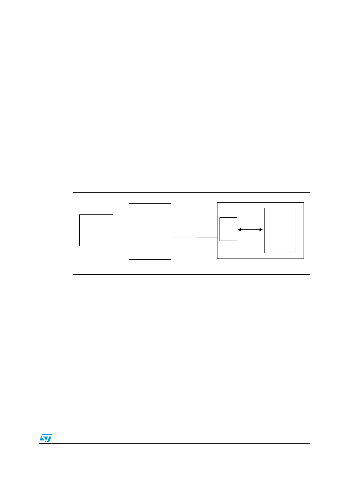
AN2737 IAP example with I2C
R/W
SCL
SDA
USB
PC + Aardvark
software
Aardvark
host adapter
STM8 device
I
2
C
Flash program
memory and
Master
Slave
data EEPROM
1 IAP example with I2C
This section describes how to perform basic IAP with the STM8 I²C peripheral. The STM8
device behaves like a standard I²C EEPROM slave which can communicate with any
master. In this application note, the Aardvark PC host adapter is used as the I²C master.
1.1 Hardware description
Figure 1 shows a typical hardware connection between the Aardvark host adapter as master
and the STM8 I²C peripheral as slave.
The Aardvark host adapter and the STM8 I²C are connected together via the data (SDA)
and clock (SCL) pins.
A 4.7 kΩ pull-up resistor must be connected to both the SDA and SCL lines
Note: If the STM8/128-EVAL board is used, the pull-up resistors are present by default.
Figure 1. Hardware connection between the Ardvark host adapter the STM8 I
1.2 Firmware description
The current firmware is provided in the ZIP file attached to this AN.
It includes:
● The I²C driver that supports all basic I²C communication.
● The Flash, GPIO, I
● STM8A and STM8S firmware libraries
The firmware uses 7-bit addressing mode which has been validated at 100 kHz and 400
kHz for the I
2
C SCL line frequency.
The STM8 address has been set to A2h using the ‘I
register is used for read/write operation selection, the value 51h must be entered in the
Aardvark software.
2
C and LCD screen drivers.
2
C
2
C own address register’. As bit 0 of this
3/16

IAP example with I2C AN2737
The firmware implements byte, word, and block programming features offered by the STM8
Flash program memory and data EEPROM.
Block programming has to be executed from the RAM memory. Consequently, at the
beginning of the code, the Flash function section is copied to the RAM memory. To copy and
link some code to the RAM memory using the Cosmic linker, the steps below must be
followed:
● Define the section to be linked in RAM as a movable segment using the linker option ‘-
ic’.
● At the begining of the code, execute the ‘_fctcpy’ function which copies the code from
the Flash to the RAM memory.
For more details about movable codes, please refer to the COSMIC “C Cross Compiler
User’s Guide for ST Microelectronics STM8” available on www.cosmicsoftware.com.
1.3 Read and write command examples
The firmware allows read or write operations in the Flash program memory (from address
8000h up to 27FFFh) or in the data EEPROM (from address 4000h up to 47FFh) memory of
the STM8.
Current and random options are available for both read and write operations:
● The random command allows data to be read/writen at a specific address.
● The current command allows data to be read/writen at the current address pointer. The
default current address pointer value (after reset) is 4000h (start of the data EEPROM).
So, for example, after writing (or reading) 10 bytes to the memory, the current address
pointer value becomes 400Ah. The address is passed on 3 bytes with the most
significant bit (MSB) first.
Note: The firmware follows standard serial I²C EEPROM protocol rules.
Before starting, the firmware example must be loaded with STVD and executed using the
run command. The evaluation board LCD displays a welcome message ‘STM8 IAP-I2C
Demo’.
1.3.1 Packet description
The different packets composing an I2C command are:
START: Start signal which is generated by the master.
ADD SLV DEVICE-W: Slave device address which is sent by the master with the direction
bit set to write.
ACK-S: Acknowledge signal which is generated by the slave.
ACK-M: Acknowledge signal which is generated by the master.
ACKF: Acknowledge failure or ‘no acknowledge’ signal which are both generated by the
master. A ‘no acknowledge’ signal is generated by the master to notify the slave device that
the last read byte has been correctly received which marks the end of a read operation.
STOP: Stop signal which is generated by the master.
4/16

AN2737 IAP example with I2C
START
ADD SLV DEVICE-R ACK-S
Bytes read from STM8
STOP
ACK-M
ACKF
1.3.2 Current read command
The current read command allows data from the Flash program memory of the STM8 to be
read, starting from the current address. This address is set to 4000h after a firmware reset.
The packet sequence to achieve a ‘current read’ is summarized in Figure 2.
Figure 2. Current read packet sequence
The following points explain how to read different bytes using the Aardvark software, starting
from the reset address (4000h):
1. Select the master tabsheet.
2. Set the bitrate to 100 kHz or 400 kHz using the ‘bitrate’ field and the ‘set’ button.
3. Set the slave address to 51h (corresponding to the firmware address A2h) in the slave
address field.
4. Uncheck the ‘10-bit addressing mode’ option because the firmware uses 7-bit
addressing mode only.
5. Uncheck the ‘no stop’ option.
6. Enter the number of bytes to be read in the ‘number of bytes’ field. A value from 1 to
255 can be entered.
7. Press the ‘master read’ button.
8. The number of bytes to be read can be changed by pressing the master read button
again.
The read values are displayed in the transaction log window of the Aardvark software.
At the end of this command, the LCD displays the message ‘reading done’.
Figure 3 illustrates points 1 to 8 of a current read command.
5/16

IAP example with I2C AN2737
Figure 3. Reading current bytes using the Aardvark software
Figure 4 shows the read values displayed in the transaction log window of the Aardvark
software.
Figure 4. Values read by the Aardvark software
6/16

AN2737 IAP example with I2C
START ADD SLV DEVICE-W ACK-S Start program address ACK-S Current read
1.3.3 Random read command
The random read command allows data from the Flash program memory or data EEPROM
of the STM8 to be read, starting from any address in the range 8000h—027FFFh or
4000h—47FFh respectively.
The packet sequence to achieve a ‘random read’ with the Aardvark software and the STM8
2
I
C is summarized in Figure 5.
Figure 5. Random read packet sequence
Two steps are required to perform a random read with the Aardvark host adapter software.
Step1 sends the first address to be read from the firmware. This is done as follows:
1. Select the master tabsheet, set the slave address and the bitrate, and uncheck the 10bit addressing mode option as per Section 1.3.2: Current read command on page 5.
2. Enter the ‘start address’ in the ‘message window’ text box. It corresponds to the first
address to be read from the Flash program memory. For example, enter ‘00 A0 00’ if
you want to read from address A000h.
3. Check the ‘no stop’ option.
4. Press the ‘master write’ button to send the start address to the firmware.
At the end of this command, the firmware has initialized its internal pointer address to the
address sent above.
7/16

IAP example with I2C AN2737
Figure 6 illustrates points 2, 3, and 4 of step1.
Figure 6. Step 1 of a random read using the Aardvark software
Step2 reads the bytes as follows:
1. Enter the number of bytes to read in the ‘number of bytes’ field. Values can be from 1 to
255.
2. Uncheck the ‘no stop’ option.
3. Press the ‘master read’ button.
4. The number of bytes to be read can be changed by pressing the master read button
again.
The read data are displayed in the transaction log window of the Aardvark software.
At the end of this command, the LCD displays the message ‘reading done’.
8/16

AN2737 IAP example with I2C
ADD SLV DEVICE-W ACK-S Bytes sent by master ACK-S STOPSTART
START ADD SLV DEVICE-W ACK-S ACK-S Current write
Start program address
1.3.4 Current write command
The current write command allows data to be written in the Flash program memory or data
EEPROM of the STM8, starting from the current address which is set to 4000h after a
firmware reset.
The packet sequence to achieve a ‘current write’ with the Aardvark software and the STM8
2
I
C is summarized in Figure 7.
Figure 7. Current write packet sequence
The following points explain how to write current bytes using the Aardvark software:
1. Select the master tabsheet, set the slave address and the bitrate, and uncheck the 10bit addressing as per Section 1.3.2: Current read command on page 5.
2. Enter the data to be writen in the Flash program memory at the current address in the
‘message window’ text box.
3. Uncheck the ‘no stop’ option.
4. Press the ‘master write’ button to send the data to the firmware.
At the end of this command, the data are written in the Flash program memory. They can be
verified using the STVD memory window. The LCD displays the message ‘writing OK’.
1.3.5 Random write command
The random write command allows data to be written in the Flash program memory or data
EEPROM of the STM8, starting from any address in the range 8000h—027FFFh or
4000h—47FFh.
The packet sequence to achieve a ‘random write’ with the Aardvark software and the STM8
2
I
C is summarized in Figure 8
Figure 8. Random write packet sequence
Two steps are required to perform a random write with the Aardvark host adapter software.
Step1 sends the first address to be writen to the firmware. This is done as follows:
1. Select the master tabsheet, set the slave address and the bitrate, and uncheck the 10bit addressing mode option as per Section 1.3.2: Current read command on page 5.
2. Enter the ‘start address’ in the ‘message window’ text box. It corresponds to the first
address to be writen to the Flash program memory.
3. Check the ‘no stop’ option.
4. Press the ‘master write’ button to send the start address to the firmware.
At the end of this command, the firmware has initialized its internal pointer address to the
address sent above.
9/16

IAP example with I2C AN2737
Step2 writes the bytes as follows:
1. Fill the data to be programmed in the ‘message window’.
2. Uncheck the ‘no stop’ option.
3. Press the ‘master write’ button.
At the end of this command, the data are written in the Flash program memory. They can be
verified using the STVD memory window. The LCD displays the message ‘writing OK’.
10/16

AN2737 IAP example with SPI
R/W
Aardvark
host adapter
USB
MOSI
MISO
SCK
SS/NSS
PC + Aardvark
software
SPI
SlaveMaster
STM8 device
Flash program
memory and
data EEPROM
2 IAP example with SPI
This section describes how to perform basic IAP with the STM8 SPI peripheral. The STM8
device behaves like a standard SPI EEPROM slave which can communicate with any
master. In this application note, the Aardvark PC host adapter is used as the SPI master.
2.1 Hardware description
Figure 9 shows a typical hardware connection between the Aardvark host adapter as master
and the STM8 SPI peripheral as slave. This type of communication uses hardware NSS
management for the slave.
The following pins are connected together:
● Aardvark MOSI and STM8 SPI MOSI.
● Aardvark MISO and STM8 SPI MISO.
● Aardvark SCK and STM8 SPI SCK.
● Aardvark SS and STM8 SPI NSS.
Note: When the STM8 evaluation board (STM8/128-EVAL) is used, the R34 resistor has to be
soldered on the R35 placement. This is to put the I/O of the micro-SD card level shifter in
high impedance state. To use the micro-SD card, the R34 resistor has to be soldered back
to its original place.
Figure 9. Hardware connection between the Ardvark host adapter and the STM8
SPI
2.2 Firmware description
The current example is provided in the ZIP file attached to this AN.
It includes:
● The SPI driver that supports all basic SPI communications.
● The Flash, CLK, GPIO and LCD screen drivers.
The STM8 clock is set to 16 MHz. The baudrate is automatically set to F
STM8 SPI peripheral is the slave). As a result, the maximum STM8 SPI speed is 8 MHz.
(because the
CPU/2
The firmware follows standard serial SPI EEPROM protocol rules. However, not all features
of a real serial SPI EEPROM are implemented here. For example, the firmware does not
11/16

IAP example with SPI AN2737
OPC-READ ADD DATA-R
00h Flash program memory data read
MOSI line
MISO line
00h
support the status register management. Consequently, it is not possible to read or write the
status register.
2.3 Read and write commands
The current example has been validated at 4 MHz for read and write operations. The
firmware allows reading or writing in the Flash program memory and data EEPROM of the
STM8 from address 8000h—027FFFh and 4000h—47FFh respectively.
Before starting, the firmware example must be loaded with STVD in the STM8 device and
executed using the run command. The evaluation board LCD displays a welcome message
‘STM8 IAP-SPI Demo’. No more messages are displayed during firmware execution.
2.3.1 Packet description
The different packets composing an SPI command are:
1. OPC-READ
2. OPC-WREN:
3. OPC-WRT
4. ADD: Physical address of the memory which is used to start a read or write operation.
5. DATA-R: Number of data to be read. It is used only for clocking (commonly these bytes
have a value of 00h).
6. DATA-W: Data to be programmed into the Flash program memory or data EEPROM.
: Opcode (03h) that requests a read.
Opcode (06h) that enables the write function.
: Opcode (02h) that requests a write after a rising NSS signal.
2.3.2 Read command
The read command allows data from the Flash program memory of the STM8 to be read,
starting from any Flash addressing range.
The packet sequence to achieve a ‘read’ with the Aardvark software and the STM8 SPI is
summarized in Figure 10. During this sequence, the NSS signal is set to GND by the
master.
Figure 10. Read packet sequence
12/16

AN2737 IAP example with SPI
The following points explain how to read different bytes using the Aardvark software:
1. Select the master tabsheet.
2. Set the bitrate to 4000 kHz using the ‘bitrate’ field and the ‘set’ button.
3. Select the polarity as rising/falling.
4. Select the phase as sample/setup.
5. Set the bit order to MSB.
6. Set the SS pin as active low (Aardvark SS pin is connected to the STM8 NSS).
7. For example, enter the following sequence: 03 00 40 00 00 00 00 00 00 00 00. The
value 03 sets the ‘read’ flag. The three bytes 00, 40, and 00 are the ‘read start
address’. The seven ‘00’ bytes correspond to the number of bytes to be read.
8. Press the ‘send’ button.
Figure 11 illustrates the different steps entered on the Aardvark software.
Figure 11. Reading bytes using the Aardvark software
Figure 12 shows the read values displayed in the transaction log window of the Aardvark
software.
Figure 12. Read values of the Aardvark software
13/16

IAP example with SPI AN2737
OPC-WREN
00h
MOSI line
MISO line
OPC-WRT ADD DATA-W
00h 00h 0x00 (1 byte per byte programmed)
MOSI line
MISO line
2.3.3 Write command
The write command allows data in the Flash program memory of the STM8 to be written,
starting from any Flash addressing range.
The packet sequence to achieve a ‘write’ with the Aardvark software and STM8 SPI is
explained below and is summarized in Figure 13 and Figure 14.
As per Section 2.3.2: Read command on page 12, select the master tabsheet, set the
bitrate (for write operations up to 8 MHz can be chosen), select the rising/falling polarity and
the sample/setup phase, and set the active low option for the SS pin.
Two steps are then required to carry out a write command.
Step 1: In the ‘message window’ text box enter the OPC-WREN value (06h) and press
‘send’. This byte is used to activate the write mode.
Step 2: In the ‘message window’ text box enter OPC-WRT ADD DATA-W and press ‘send’.
For example, 02 01 90 FF AA 55 BB 66 programs 4 bytes starting from address 0190FFh.
Figure 13. Step 1 of the write packet sequence using Aardvark software
Figure 14. Step 2 of the write packet sequence using Aardvark software
In step 2, a maximun of 128 bytes can be programmed. When step 2 is finished, the NSS
signal rises up and the Flash is programmed with the DATA-W bytes at the ADD address.
At the end of this command, the data are written in the Flash memory. They can be verified
using the STVD memory window or by performing an SPI read.
14/16

AN2737 Revision history
3 Revision history
Table 1. Document revision history
Date Revision Changes
02-May-2008 1 Initial release
Changed document title.
Reformulated text of the Introduction to improve understanding and
readability.
13-Nov-2008 2
02-Mar-2009 3
Changed all references of the ‘STM8 firmware’ to the ‘
STM8S
Changed all references of ‘Aardvark-I2C’ and ‘Aardvark-SPI’ to
‘Aardvark’.
Updated document title.
Current firmware is provided as a zip attachment with this application
note (and not in the STM8 firmware libraries).Throughout the
document, firmware descriptions and examples have been updated
to reflect the new source code.
Modified text throughout document (without changing technical
content) to improve clarity and readability.
Updated terminology: Program memory replaced by Flash program
memory and data memory replaced by data EEPROM.
Section 1.2: Firmware description: Added information concerning
byte, word, and block programming features offered by the STM8.
Section 1.3: Read and write command examples: Added that read
and write operations are possible from both the Flash program
memory and the data EEPROM; provided address range for both;
added note that the firmware follows standard serial I
protocol rules.
Section 1.3.2: Current read command: Current address of the Flash
program memory after a firmware reset changed from 8000h to
4000h; updated frequency; updated and replaced Figure 3 and
Figure 4.
Section 1.3.3: Random read command: Clarified that random read
commands are possible from both the Flash program memory and
data EEPROM; provided address range for both; replaced example
addresses in ‘step 1’; updated and replaced Figure 6.
Section 1.3.4: Current write command: Clarified that current write
commands are possible from both the Flash program memory and
data EEPROM starting from the current address (which was
updated).
Section 1.3.5: Random write command: Clarified that random write
commands are possible from both the Flash program memory and
data EEPROM; provided address range for both.
Section 2.1: Hardware description: Added note about using the
STM8/128-EVAL evaluation board.
Section 2.3: Read and write commands: Updated frequency for read
and write operations.
Section 2.3.2: Read command: Updated Figure 10; updated and
replaced Figure 11 and Figure 12.
firmwares’.
STM8A and
2
C EEPROM
15/16

AN2737
Please Read Carefully:
Information in this document is provided solely in connection with ST products. STMicroelectronics NV and its subsidiaries (“ST”) reserve the
right to make changes, corrections, modifications or improvements, to this document, and the products and services described herein at any
time, without notice.
All ST products are sold pursuant to ST’s terms and conditions of sale.
Purchasers are solely responsible for the choice, selection and use of the ST products and services described herein, and ST assumes no
liability whatsoever relating to the choice, selection or use of the ST products and services described herein.
No license, express or implied, by estoppel or otherwise, to any intellectual property rights is granted under this document. If any part of this
document refers to any third party products or services it shall not be deemed a license grant by ST for the use of such third party products
or services, or any intellectual property contained therein or considered as a warranty covering the use in any manner whatsoever of such
third party products or services or any intellectual property contained therein.
UNLESS OTHERWISE SET FORTH IN ST’S TERMS AND CONDITIONS OF SALE ST DISCLAIMS ANY EXPRESS OR IMPLIED
WARRANTY WITH RESPECT TO THE USE AND/OR SALE OF ST PRODUCTS INCLUDING WITHOUT LIMITATION IMPLIED
WARRANTIES OF MERCHANTABILITY, FITNESS FOR A PARTICULAR PURPOSE (AND THEIR EQUIVALENTS UNDER THE LAWS
OF ANY JURISDICTION), OR INFRINGEMENT OF ANY PATENT, COPYRIGHT OR OTHER INTELLECTUAL PROPERTY RIGHT.
UNLESS EXPRESSLY APPROVED IN WRITING BY AN AUTHORIZED ST REPRESENTATIVE, ST PRODUCTS ARE NOT
RECOMMENDED, AUTHORIZED OR WARRANTED FOR USE IN MILITARY, AIR CRAFT, SPACE, LIFE SAVING, OR LIFE SUSTAINING
APPLICATIONS, NOR IN PRODUCTS OR SYSTEMS WHERE FAILURE OR MALFUNCTION MAY RESULT IN PERSONAL INJURY,
DEATH, OR SEVERE PROPERTY OR ENVIRONMENTAL DAMAGE. ST PRODUCTS WHICH ARE NOT SPECIFIED AS "AUTOMOTIVE
GRADE" MAY ONLY BE USED IN AUTOMOTIVE APPLICATIONS AT USER’S OWN RISK.
Resale of ST products with provisions different from the statements and/or technical features set forth in this document shall immediately void
any warranty granted by ST for the ST product or service described herein and shall not create or extend in any manner whatsoever, any
liability of ST.
ST and the ST logo are trademarks or registered trademarks of ST in various countries.
Information in this document supersedes and replaces all information previously supplied.
The ST logo is a registered trademark of STMicroelectronics. All other names are the property of their respective owners.
© 2009 STMicroelectronics - All rights reserved
STMicroelectronics group of companies
Australia - Belgium - Brazil - Canada - China - Czech Republic - Finland - France - Germany - Hong Kong - India - Israel - Italy - Japan -
Malaysia - Malta - Morocco - Singapore - Spain - Sweden - Switzerland - United Kingdom - United States of America
www.st.com
16/16
 Loading...