

Page 1

AN2734
Application note
S-Touch™ design procedure
Introduction
The purpose of this application note is to provide the system/hardware engineers enough
ground knowledge to start the design of capacitive touch inferface solutions with the
S-Touch
The document highlights the recommended step-by-step procedures to be followed for a
successful S-Touch
production and production tests.
Each topic covered in this document is explained in detail in other application notes.
™ capacitive controller devices.
™ design-in: design flow, PCB layout, fabrication, assembly pre-
January 2010 Doc ID 14573 Rev 2 1/14
www.st.com
Page 2

Contents AN2734
Contents
1 Touch module design flow . . . . . . . . . . . . . . . . . . . . . . . . . . . . . . . . . . . . 3
1.1 Touch module specifications . . . . . . . . . . . . . . . . . . . . . . . . . . . . . . . . . . . 4
2 PCB layout, fabrication and assembly . . . . . . . . . . . . . . . . . . . . . . . . . . 6
2.1 Pre-production tuning/test . . . . . . . . . . . . . . . . . . . . . . . . . . . . . . . . . . . . . 7
2.1.1 Hardware tuning . . . . . . . . . . . . . . . . . . . . . . . . . . . . . . . . . . . . . . . . . . . 7
2.1.2 Software tuning . . . . . . . . . . . . . . . . . . . . . . . . . . . . . . . . . . . . . . . . . . . . 8
2.2 Production test . . . . . . . . . . . . . . . . . . . . . . . . . . . . . . . . . . . . . . . . . . . . . 10
3 Conclusion . . . . . . . . . . . . . . . . . . . . . . . . . . . . . . . . . . . . . . . . . . . . . . . . 11
4 Reference . . . . . . . . . . . . . . . . . . . . . . . . . . . . . . . . . . . . . . . . . . . . . . . . . 12
5 Revision history . . . . . . . . . . . . . . . . . . . . . . . . . . . . . . . . . . . . . . . . . . . 13
2/14 Doc ID 14573 Rev 2
Page 3

AN2734 Touch module design flow
1 Touch module design flow
Figure 1 shows a simplified flowchart which describes the complete touch module design
flow starting from the specification to the mass production test of the PCB and the overall
system.
Figure 1. Touch module design flow
Spec ification
Dev ice
selection
Schematic
Specification review
layout, fab & ass embly
System integration test
PCB
Hardware
tuning
(s oftware tuning)
Mass production
(produc tion test)
PCB revision
GC25419
Doc ID 14573 Rev 2 3/14
Page 4
Touch module design flow AN2734
1.1 Touch module specifications
Before starting the design of a capacitive touch module, a clear specification should be
defined to establish:
● Touchkeys number and functions
● Slider/rotator implementation
● LED backlighting - white LEDs or red LEDs, 5 V system or 3.6 V system etc
● Signal connections to the host system
● Module form factor
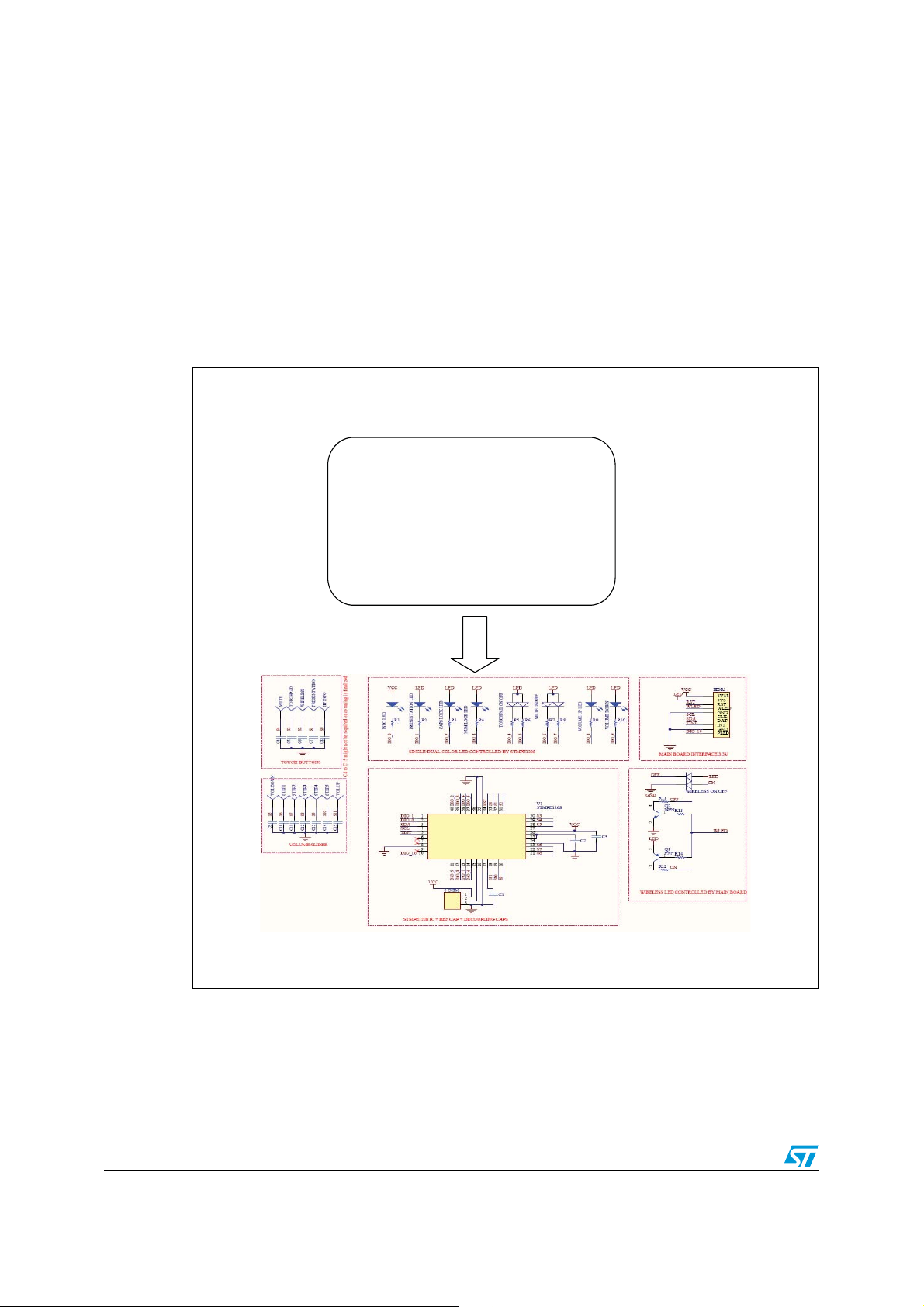
Figure 2. Specification definitions to schematic implementation
Keys
Slider/rotator
Specifications:
Backlighting led
Connection to host
Form factor
PCB
The next step to be performed after finalizing the module specification is to choose the most
appropriate device from the S-Touch product family, based on the requirements of the target
application.
4/14 Doc ID 14573 Rev 2
Page 5

AN2734 Touch module design flow
The S-Touch devices have several sensor channels and various features. The STMPE821,
for example, consists of 8 I/Os that can be used as either normal input/outputs or as touch
sensor inputs. On a particular application, out of the eight I/Os, four I/Os can be used as
capacitive touch key input and the other four can be used for the backlighting LED control. If
the I/O is used for LED control, it can be configured as PWM output to create elaborate LED
effects.
Figure 3. STMPE821 block diagram
INT
RST
SCLK
SDAT
GPIO
controller
interface
GND VCC VIO
PWM
controller
I2 C
Impedance
Touchkey
controller
sensor
GPIO 0 - 7
/Touch 0 - 7
ARef
CS00046
For further details on S-Touch working principles and functional features, please refer to the
application note AN2693: "S-Touch
TM
devices: system considerations".
Doc ID 14573 Rev 2 5/14
Page 6

PCB layout, fabrication and assembly AN2734
2 PCB layout, fabrication and assembly
Measuring the capacitance of a sensor is quite simple. However, in order to obtain a reliable
measurement of finger capacitance, in-depth technical knowledge is required.
Two conductive materials such as wire, traces or metal that are at different potentials and in
close proximity to one another act as a conductive plate, forming a capacitor. Therefore,
when designing the layout for the touch module PCB, some standard guidelines should be
followed to route the sensor traces. Otherwise, crosstalk and disturbances between sensors
and wires, traces and the metal plate reduce touch module performance.
Periodic sampling signals are used to measure the sensors’ electrode capacitance. The
presence of noise might disturb the sensing of the signal and cause false detection in touch
keys and incorrect location reading in sliders or rotators.The controller IC can filter a low to
moderate amount of noise. It is therefore recommended to design the PCB layout in such a
way that the interaction between the external noise and the sensor/electrode circuitry is
minimized.
There are a few different types of sensor electrodes: button, slider, rotator, matrix key and
touch pad. Each one serves a specific function. Their shapes and sizes differ based on the
application and form factor requirements.
Figure 4. Sensor electrodes
For further details on the PCB and layout considerations, please refer to application note
AN2733 “S-Touch
TM
PCB and layout guidelines”.
6/14 Doc ID 14573 Rev 2
Page 7

AN2734 PCB layout, fabrication and assembly
2.1 Pre-production tuning/test
Once the PCB fabrication is complete, the S-Touch controller IC and the passive
components are assembled on the PCB.
2.1.1 Hardware tuning
The reference and input tuning capacitors are populated on the PCB as part of a process
called “hardware tuning”. This process is required due to the imbalance in the inherent
capacitance between the capacitive lines (reference and sensor inputs, see Figure 5). The
objective of the hardware tuning is to bring the no-touch impedance of all the unused sensor
inputs within the dynamic range for touch detection.
Figure 5. Imbalanced inherent capacitance
2EF
The hardware tuning process is described more in detail in the application note AN2801Hardware tuning procedures.
Figure 6. Dynamic range tuning software
As shown in Figure 6, the hardware tuning process can be achieved more easily by using
the provided software.
Doc ID 14573 Rev 2 7/14
Page 8

PCB layout, fabrication and assembly AN2734
2.1.2 Software tuning
The next step is software tuning. The S-Touch devices are register-based which means that
the host must configure the device for it to work properly. It is suggested to perform the
software tuning with the panel overlay attached to the PCB and with the touch module
assembled on the system.
When the touch module is assembled on the system, interactions with other components
and noise on the system affect the operation. This is why the software tuning is performed
on the system and not on the standalone touch module.
During the software tuning, the registers which control the sensitivity, noise filtering,
calibration and some other related registers are tuned to get optimum values. Once the
correct register values are tuned/validated properly, they are embedded as part of the host
system code. Each time the system is powered up, the host initializes the S-Touch device
with these register values.
The final register values validated during the software tuning process provide the optimal
configuration for the S-Touch registers, allowing the device to work properly in any condition.
Figure 7. Signal-to-noise ratio measurement
The system integration tests cover the signal-to-noise ratio measurement (Figure 7), water
drop tests for systems operating in wet environments and touch failure ratio. It includes
susceptibility to external disturbances such as external RF noise, effect of fluorescent lamp
emissions, mobile phone emisissions, etc.
8/14 Doc ID 14573 Rev 2
Page 9

AN2734 PCB layout, fabrication and assembly
Figure 8. Signal-to-noise ratio tool
For complete software tuning guidelines, please refer to the application notes AN2802 “STouch registers descriptions” and AN2805 "System integration test".
Doc ID 14573 Rev 2 9/14
Page 10

PCB layout, fabrication and assembly AN2734
2.2 Production test
The production test consists of a module production test and a system integration
production test.
The module production test is performed on the touch module PCB (without overlay panel)
in order to screen any assembly and/or components failures.
The system production test is performed with the touch module (attached to the overlay
panel) assembled on the system.
Figure 9. Mass production test tool
The system integration production tests can be performed automatically or manually. An
automated test can be carried out using a metallic plate to simulate a finger touch and a
manual test can be performed with a production operator manually touching the button to
test its functionalities.
10/14 Doc ID 14573 Rev 2
Page 11

AN2734 Conclusion
3 Conclusion
Below is a short summary table on the S-Touch design procedure.
Table 1. S-Touch design procedure
Step Description Notes STMicroelectronics tools
Define number of
System level functional
1
definition
Schematic design and PCB
2
layout
buttons/slider/wheel,
approximate placement, board
size, cover thickness/material
Device selection, number of
PCBs layers
PCB layout guidelines
Assembly of 5-10 boards for
3
capacitance tuning
Software
4
development/optimization
based on 5-10 boards
Assembly of 100-200
5
boards according to tuning
results (step 3)
Analysis of test (MP test,
SNR test, noise test) results
6
from 100-200 sets.
Fine tuning of capacitance
values if necessary
Tuning done with actual cover
material
Noise immunity
setting,optimized sensitivity
setting, SNR test
To check consistency/stability
of the capacitive module in
actual production condition
Results should be consistent
with system level requirements
Dynamic range tuning tool
Reference code, software
tuning tool, SNR tool
Mass production test software
toolkit
Doc ID 14573 Rev 2 11/14
Page 12

Reference AN2734
4 Reference
1. STMPE821 datasheet
2. STMPE1208S datasheet
3. AN2693, S-Touch
4. AN2733, S-Touch
5. AN2801, Hardware tuning procedures
6. AN2802, A programming guide for the touch module in capacitive S-Touch™ devices
7. AN2805, System integration test
™ devices: system considerations
™ PCB and layout guidelines
12/14 Doc ID 14573 Rev 2
Page 13

AN2734 Revision history
5 Revision history
Table 2. Document revision history
Date Revision Changes
30-Apr-2009 1 Initial release.
15-Jan-2010 2 Removed reference to AN2806.
Doc ID 14573 Rev 2 13/14
Page 14

AN2734
Please Read Carefully:
Information in this document is provided solely in connection with ST products. STMicroelectronics NV and its subsidiaries (“ST”) reserve the
right to make changes, corrections, modifications or improvements, to this document, and the products and services described herein at any
time, without notice.
All ST products are sold pursuant to ST’s terms and conditions of sale.
Purchasers are solely responsible for the choice, selection and use of the ST products and services described herein, and ST assumes no
liability whatsoever relating to the choice, selection or use of the ST products and services described herein.
No license, express or implied, by estoppel or otherwise, to any intellectual property rights is granted under this document. If any part of this
document refers to any third party products or services it shall not be deemed a license grant by ST for the use of such third party products
or services, or any intellectual property contained therein or considered as a warranty covering the use in any manner whatsoever of such
third party products or services or any intellectual property contained therein.
UNLESS OTHERWISE SET FORTH IN ST’S TERMS AND CONDITIONS OF SALE ST DISCLAIMS ANY EXPRESS OR IMPLIED
WARRANTY WITH RESPECT TO THE USE AND/OR SALE OF ST PRODUCTS INCLUDING WITHOUT LIMITATION IMPLIED
WARRANTIES OF MERCHANTABILITY, FITNESS FOR A PARTICULAR PURPOSE (AND THEIR EQUIVALENTS UNDER THE LAWS
OF ANY JURISDICTION), OR INFRINGEMENT OF ANY PATENT, COPYRIGHT OR OTHER INTELLECTUAL PROPERTY RIGHT.
UNLESS EXPRESSLY APPROVED IN WRITING BY AN AUTHORIZED ST REPRESENTATIVE, ST PRODUCTS ARE NOT
RECOMMENDED, AUTHORIZED OR WARRANTED FOR USE IN MILITARY, AIR CRAFT, SPACE, LIFE SAVING, OR LIFE SUSTAINING
APPLICATIONS, NOR IN PRODUCTS OR SYSTEMS WHERE FAILURE OR MALFUNCTION MAY RESULT IN PERSONAL INJURY,
DEATH, OR SEVERE PROPERTY OR ENVIRONMENTAL DAMAGE. ST PRODUCTS WHICH ARE NOT SPECIFIED AS "AUTOMOTIVE
GRADE" MAY ONLY BE USED IN AUTOMOTIVE APPLICATIONS AT USER’S OWN RISK.
Resale of ST products with provisions different from the statements and/or technical features set forth in this document shall immediately void
any warranty granted by ST for the ST product or service described herein and shall not create or extend in any manner whatsoever, any
liability of ST.
ST and the ST logo are trademarks or registered trademarks of ST in various countries.
Information in this document supersedes and replaces all information previously supplied.
The ST logo is a registered trademark of STMicroelectronics. All other names are the property of their respective owners.
© 2010 STMicroelectronics - All rights reserved
STMicroelectronics group of companies
Australia - Belgium - Brazil - Canada - China - Czech Republic - Finland - France - Germany - Hong Kong - India - Israel - Italy - Japan -
Malaysia - Malta - Morocco - Philippines - Singapore - Spain - Sweden - Switzerland - United Kingdom - United States of America
www.st.com
14/14 Doc ID 14573 Rev 2
 Loading...