

Page 1
AN2728
Application note
ST1S12
small synchronous buck converter
Introduction
The ST1S12 family of synchronous step-down DC-DC converters optimized for powering
low-voltage digital cores in HDD applications is generally used to replace the high-current
linear solution when the power dissipation may cause high heating of the application
environment. It provides up to 0.7 A over an input voltage range of 2.5 V to 5.5 V.
A high switching frequency (1.7 MHz) allows the use of tiny surface-mount components. A
resistor divider to set the output voltage value, an inductor, and two capacitors are required
for the adjustable version. Only an inductor and 2 capacitors are needed for the 1.2 V and
1.8 V fixed version. A low output ripple is guaranteed by the current mode PWM topology
and by the use of low ESR surface-mount ceramic capacitors.
The device is thermal protected and current limited to prevent damages due to accidental
short-circuit. This family of products is available in the TSOT23-5L package.
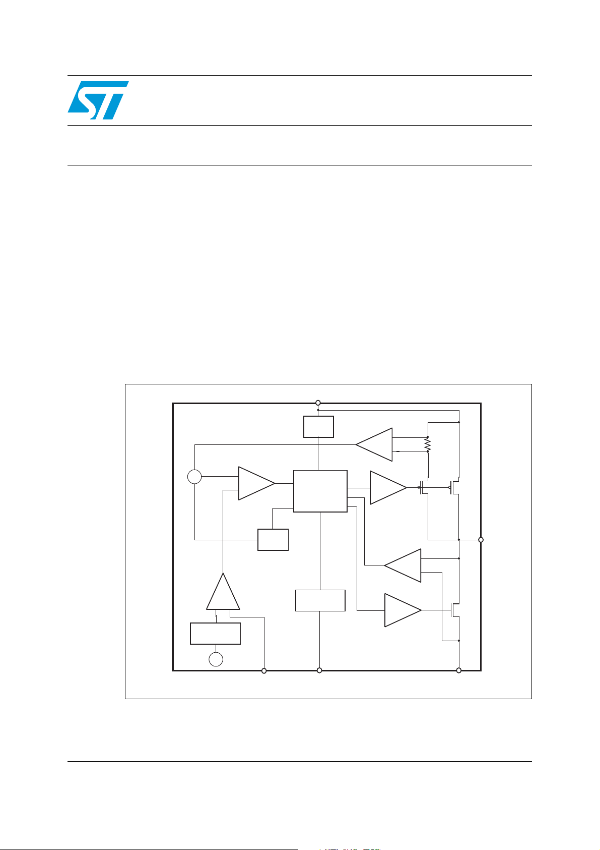
Figure 1. ST1S12 - simplified schematic
V
IN
VSUM
Σ
VC
g
m
+
-
SOFT START
REF1
Comp
FB/V
OSC
O
RST
V
VSET
UVLO
MOSFET
CONTROL
LOGIC
SHUT DOWN
EN
VDRV_P
VDRV_N
I_SEN
Driver
DMD
+
-
DMD
Driver
R
sense
SW
+
-
Gnd
April 2008 Rev 1 1/20
www.st.com
20
Page 2

Contents AN2728
Contents
1 ST1S12 description . . . . . . . . . . . . . . . . . . . . . . . . . . . . . . . . . . . . . . . . . . 4
1.1 Enable function . . . . . . . . . . . . . . . . . . . . . . . . . . . . . . . . . . . . . . . . . . . . . . 5
1.2 Current limit and short-circuit protection . . . . . . . . . . . . . . . . . . . . . . . . . . 6
2 Selecting components for your applications . . . . . . . . . . . . . . . . . . . . . 7
2.1 Output voltage selection . . . . . . . . . . . . . . . . . . . . . . . . . . . . . . . . . . . . . . . 7
2.2 Input capacitor . . . . . . . . . . . . . . . . . . . . . . . . . . . . . . . . . . . . . . . . . . . . . . 8
2.3 Output capacitor . . . . . . . . . . . . . . . . . . . . . . . . . . . . . . . . . . . . . . . . . . . . . 9
2.4 Inductor . . . . . . . . . . . . . . . . . . . . . . . . . . . . . . . . . . . . . . . . . . . . . . . . . . . 9
2.5 Layout considerations . . . . . . . . . . . . . . . . . . . . . . . . . . . . . . . . . . . . . . . . 10
3 Thermal considerations . . . . . . . . . . . . . . . . . . . . . . . . . . . . . . . . . . . . . 11
4 Demonstration board usage recommendation . . . . . . . . . . . . . . . . . . . 13
4.1 External component selection . . . . . . . . . . . . . . . . . . . . . . . . . . . . . . . . . 14
4.2 Capacitors selection . . . . . . . . . . . . . . . . . . . . . . . . . . . . . . . . . . . . . . . . . 14
4.3 Inductor selection . . . . . . . . . . . . . . . . . . . . . . . . . . . . . . . . . . . . . . . . . . . 15
5 Bill of materials . . . . . . . . . . . . . . . . . . . . . . . . . . . . . . . . . . . . . . . . . . . . 17
6 Recommended footprint . . . . . . . . . . . . . . . . . . . . . . . . . . . . . . . . . . . . . 18
7 Revision history . . . . . . . . . . . . . . . . . . . . . . . . . . . . . . . . . . . . . . . . . . . 19
2/20
Page 3

AN2728 List of figures
List of figures
Figure 1. ST1S12 - simplified schematic . . . . . . . . . . . . . . . . . . . . . . . . . . . . . . . . . . . . . . . . . . . . . . . 1
Figure 2. Inductor current at no load . . . . . . . . . . . . . . . . . . . . . . . . . . . . . . . . . . . . . . . . . . . . . . . . . . 4
Figure 3. Inductor current at medium load . . . . . . . . . . . . . . . . . . . . . . . . . . . . . . . . . . . . . . . . . . . . . . 4
Figure 4. Inrush current . . . . . . . . . . . . . . . . . . . . . . . . . . . . . . . . . . . . . . . . . . . . . . . . . . . . . . . . . . . . 4
Figure 5. Enable voltage vs. temperature . . . . . . . . . . . . . . . . . . . . . . . . . . . . . . . . . . . . . . . . . . . . . . 5
Figure 6. Short-circuit protection simplified schematic. . . . . . . . . . . . . . . . . . . . . . . . . . . . . . . . . . . . . 6
Figure 7. Typical application schematic . . . . . . . . . . . . . . . . . . . . . . . . . . . . . . . . . . . . . . . . . . . . . . . . 7
Figure 8. Drop vs. temperature . . . . . . . . . . . . . . . . . . . . . . . . . . . . . . . . . . . . . . . . . . . . . . . . . . . . . . 7
Figure 9. Feedback voltage vs. temperature . . . . . . . . . . . . . . . . . . . . . . . . . . . . . . . . . . . . . . . . . . . . 8
Figure 10. Layout considerations . . . . . . . . . . . . . . . . . . . . . . . . . . . . . . . . . . . . . . . . . . . . . . . . . . . . . 10
Figure 11. ST1S12 demonstration board layout . . . . . . . . . . . . . . . . . . . . . . . . . . . . . . . . . . . . . . . . . 13
Figure 12. Demonstration board layers . . . . . . . . . . . . . . . . . . . . . . . . . . . . . . . . . . . . . . . . . . . . . . . . 13
Figure 13. Demonstration board schematic . . . . . . . . . . . . . . . . . . . . . . . . . . . . . . . . . . . . . . . . . . . . . 14
Figure 14. Efficiency vs. output current . . . . . . . . . . . . . . . . . . . . . . . . . . . . . . . . . . . . . . . . . . . . . . . . 15
Figure 15. Efficiency vs. output voltage . . . . . . . . . . . . . . . . . . . . . . . . . . . . . . . . . . . . . . . . . . . . . . . . 15
Figure 16. Efficiency vs. inductor at V
Figure 17. Efficiency vs. inductor at V
Figure 18. Efficiency vs. input voltage . . . . . . . . . . . . . . . . . . . . . . . . . . . . . . . . . . . . . . . . . . . . . . . . . 16
Figure 19. TSOT23-5L footprint dimensions . . . . . . . . . . . . . . . . . . . . . . . . . . . . . . . . . . . . . . . . . . . . 18
= 1.8 V . . . . . . . . . . . . . . . . . . . . . . . . . . . . . . . . . . . . . . . . . . 16
O
= 3.3 V . . . . . . . . . . . . . . . . . . . . . . . . . . . . . . . . . . . . . . . . . . 16
O
3/20
Page 4
ST1S12 description AN2728
1 ST1S12 description
The ST1S12 is an adjustable current mode PWM synchronous step-down DC-DC converter
with an internal 0.7 A power switch. It is a complete 0.7 A switching regulator with internal
compensation which eliminates the need for additional components.
The device operates with typically 1.7 MHz fixed frequency, and in order to guarantee the
lowest switching ripple, operates in pulse width modulation (PWM) mode even at low-load
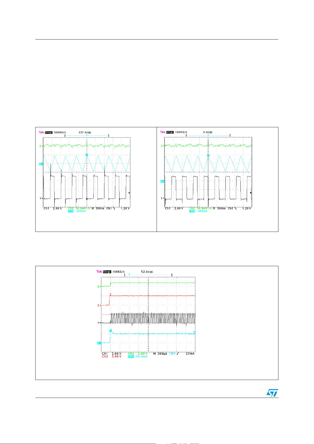
condition. (Figure 2 and Figure 3)
Figure 2. Inductor current at no load Figure 3. Inductor current at medium load
VEN=VIN=5 V, V
OUT
, CH4=I
CH2=V
=1.8 V, no load, CH1=SW,
OUT
L
To clamp the error amplifier reference voltage, a soft-start control block generating a voltage
ramp is implemented. When switching on the power supply, it allows controlling the inrush
current value (Figure 4).
Figure 4. Inrush current
V
I
L
SW
OUT
(AC)
VEN=VIN=5 V, V
CH2=V
OUT
, CH4=I
OUT
L
V
EN
=1.8 V, R
OUT
=4.7 Ω, CH1=SW,
LOAD
Vout (AC)
I
L
SW
4/20
VEN=VIN=5 V, V
Ch1=SW, CH2=V
=1.8 V, R
OUT
, CH3=EN, CH4=I
OUT
LOAD
=15 Ω,
IN
SW
I
IN
Page 5
AN2728 ST1S12 description
Other protection circuits in the device are the thermal shutdown block which turns off the
regulator when the junction temperature exceeds 150 °C (typ.) and the cycle-by-cycle
current limiting that provides protection against shorted outputs.
The few components required for operation of the device are an inductor, two capacitors,
and a resistor divider. The inductor chosen must be capable of withstanding peak current
level without saturating. The value of the inductor should be selected keeping in mind that a
large inductor value increases the efficiency at low output current and reduces output
voltage ripple, while a smaller inductor can be chosen when it is important to reduce the
package size and the total application cost. The ST1S12 has been designed to work
properly with X5R or X7R SMD ceramic capacitors both at the input and at the output.
These types of capacitors, thanks to their very low series resistance (ESR), minimize the
output voltage ripple. Other low ESR capacitors can be used according to the need of the
application without compromising the right functioning of the device.
Finally, if the input voltage falls close to the output voltage, the ST1S12 can run at 100 %
duty cycle, in this mode the PMOS switch is continuously maintained ON. In this case the
output voltage value is the input voltage minus the voltage drop across the PMOS switch
and the resistance of the inductor.
The minimum input voltage to guarantee the right output voltage is:
where DCR
V
is DC resistance of the inductor and R
L
IN_MIN
= I
OUT_MAX
Due to the high switching frequency and peak current, it is important to optimize the
application environment such as reducing the length of the PCB traces and placing all
external components near the device.
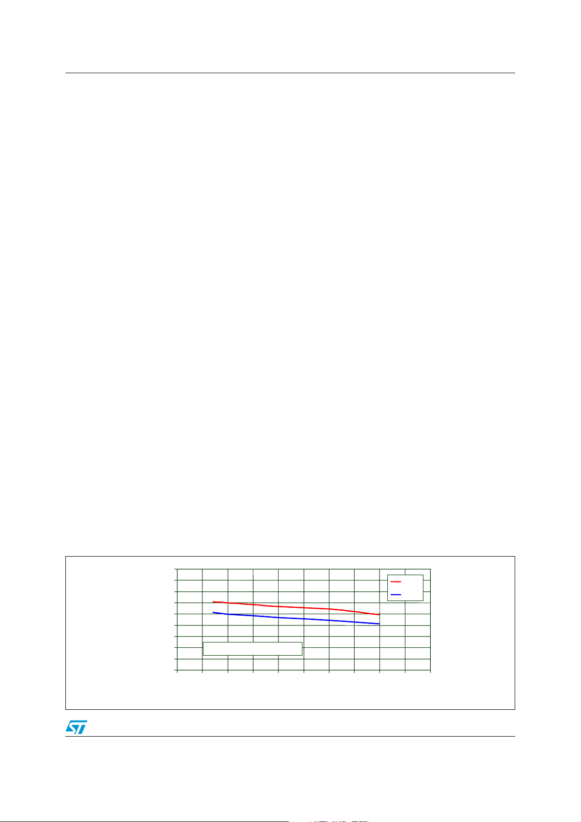
1.1 Enable function
The ST1S12 features an enable function (pin 1). When the EN voltage is higher than 1.5 V
the device is ON and if it is lower than 0.5 V the device is OFF, Figure 5 shows the enable
voltage vs temperature. In shutdown mode consumption is lower than 1 µA.
The EN pin does not have an internal pull-up, which means that the enable pin cannot be
left floating.
If the enable function is not used, the EN pin must be connected to V
Figure 5. Enable voltage vs. temperature
1.8
1.8
1.6
1.6
1.4
1.4
1.2
1.2
[V]
[V]
1
1
EN
EN
0.8
0.8
V
V
0.6
0.6
0.4
0.4
0.2
0.2
0
0
-75 -50 -25 0 25 50 75 100 125 150 175
-75 -50 -25 0 25 50 75 100 125 150 175
V
V
IN
IN
= 5.5 V, I
= 5.5 V, I
OUT
OUT
= 10 mA
= 10 mA
x (R
T [°C]
T [°C]
DS(on)_P
+ DCRL) + V
DS(on)_P
is the resistance of the PMOS.
OUT
ON
ON
OFF
OFF
IN.
5/20
Page 6
ST1S12 description AN2728
1.2 Current limit and short-circuit protection
In overcurrent protection mode, when the peak current reaches the current limit, the device
reduces t
reduced and, in most applications, this is enough to limit the current to I
In case of heavy short-circuit when the feedback voltage is lower than 0.1 V (typ.), the loop
switches to short mode automatically. In this condition the voltage V
compared with 0.4 V (typ.) to clamp the upper limit of the inductor current. In this condition
the maximum output limitation current is reduced to 300 mA instead of 1 A. At the same time
the DMD circuit clamps the lower boundary of the inductor current. One RS flip-flop is being
used to control the PMOS and NMOS switches. When the feedback voltage is higher than
0.1 V (typ.) voltage, the device returns to normal closed-loop switching operation (Figure 6).
Figure 6. Short-circuit protection simplified schematic
V
V
sum=Isen*Rsen
sum=Isen*Rsen
V
V
REF1
REF1
V
V
C
C
COM
COM
-
-
+
+
down to its minimum value. In these conditions, the duty cycle is strongly
ON
+
+
COM
COM
-
-
S
S
R
R
DMD
DMD
V
V
IN
IN
L1
Q
Q
-
-
+
+
L1
.
lim
sum=Isen
* R
R1
R1
R2
R2
sen
V
V
is
OUT
OUT
C2
C2
0.1V
0.1V
GND
V
V
FB
FB
GND
GND
GND
GND
GND
6/20
Page 7

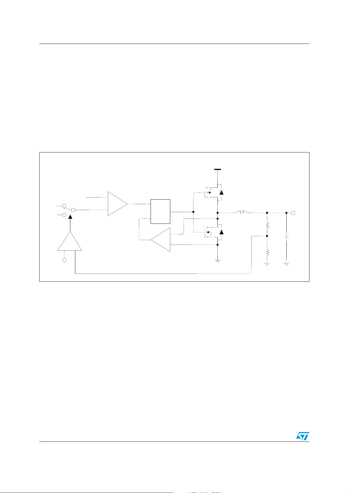
AN2728 Selecting components for your applications
2 Selecting components for your applications
This section provides information to assist in the selection of the most appropriate
components for your applications.
Figure 7 shows the typical application schematic.
Figure 7. Typical application schematic
V
V
IN
IN
OFF ON
OFF ON
C1
C1
V
V
4
4
IN
IN
ST1S12_ADJ
ST1S12_ADJ
3
3
SW
VFB
VFB
5
5
SW
R1
R1
EN
EN
1
1
GND
GND
2
2
L1
L1
V
V
OUT
OUT
2.1 Output voltage selection
The output voltage can be adjusted from 0.6 V up to input voltage (D
voltage drop across the PMOS switch and the DC resistance of the inductor by connecting a
resistor divider between the V
Figure 8. Drop vs. temperature
0.5
0.5
0.4
0.4
0.3
0.3
0.2
0.2
Drop [V]
Drop [V]
0.1
0.1
0
0
-75 -50 -25 0 25 50 75 100 125 150 175
-75 -50 -25 0 25 50 75 100 125 150 175
pin and the output, thus allowing remote voltage sensing.
FB
V
= 2.7 V, I
V
= 2.7 V, I
OUT
OUT
R2
R2
GND
GND
= 700 mA, Duty cycle = 100%
= 700 mA, Duty cycle = 100%
OUT
OUT
T [°C]
T [°C]
C2
C2
= 100 %) minus the
MAX
7/20
Page 8

Selecting components for your applications AN2728
You must choose the resistor divider according to the following equation:
Equation 1
R
R
1
1
+=
+=
1VV
1VV
FBOUT
FBOUT
R
R
[]
[]
2
2
with V
= 0.6 V.
FB
Figure 9 shows the feedback voltage versus temperature.
Figure 9. Feedback voltage vs. temperature
650
650
630
630
610
610
[mV]
[mV]
FB
FB
590
590
V
V
570
570
550
550
-75 -50 -25 0 25 50 75 100 125 150 175
-75 -50 -25 0 25 50 75 100 125 150 175
We suggest using a resistor with values in the range of 10 kΩ to 100 kΩ. Lower values are
suitable as well but increase current consumption.
For output voltages close to the feedback voltage, we suggest adding a very small capacitor
in parallel with R
in the range of 10 pF. As an alternative, we suggest increasing the current
1
in the resistor divider by decreasing the R
V
= 3.6 V, I
V
= 3.6 V, I
IN
IN
T [°C]
T [°C]
and R2 value.
1
OUT
OUT
= 10 mA
= 10 mA
2.2 Input capacitor
The input capacitor must be able to support the maximum input operating voltage and the
maximum RMS input current.
Since step-down converters draw current from the input in pulses, the input current is
squared and the height of each pulse is equal to the output current. The input capacitor has
to absorb switching current that can be as high as the load current divided by two (worst
case, with duty cycle of 50 %). For this reason, the quality of these capacitors has to be very
high to minimize its power dissipation generated by the internal ESR, thus improving the
system reliability and efficiency. The critical parameter is usually the RMS current rating,
which must be higher than the RMS input current. The maximum RMS input current (flowing
through the input capacitor) is:
Equation 2
where η is the expected system efficiency, D is the duty cycle and I
current. This function reaches its maximum value at D = 0.5 and the equivalent RMS current
is equal to I
8/20
divided by 2 (considering η = 1).
OUT
22
×
×
-×=
-×=
DII
OUTRMS
OUTRMS
DII
η
η
22
D
D2
D
D2
+
+
η
η
the output DC
OUT
Page 9

AN2728 Selecting components for your applications
The maximum and minimum duty cycles are:
Equation 3
+
+
VV
VV
FOUT
=
=
D
D
MAX
MAX
FOUT
-
-
VV
VV
SWINMIN
SWINMIN
and
Equation 4
+
+
VV
VV
FOUT
=
=
D
D
MAX
MAX
FOUT
-
-
VV
VV
SWINMAX
SWINMAX
where V
it is the voltage drop across the internal NMOS and VSW the voltage drop across
F
the internal PMOS. Considering the range D
maximum I
flowing through the input capacitor.
RMS
The use of ceramic capacitors with voltage ratings in the range of 1.5 times the maximum
output voltage is recommended.
2.3 Output capacitor
The output capacitor is very important to satisfy the output voltage ripple requirement. Using
a small inductor value is useful to reduce the size of the coil, but increases the current ripple.
So, in order to reduce the output voltage ripple a low ESR capacitor is required. The output
voltage ripple (V
OUT_RIPPLE
Equation 5
where ∆ I is the ripple current and F
The use of ceramic capacitors with voltage ratings in the range of 1.5 times the maximum
output voltage is recommended.
) is:
V
V
_
_
to D
MIN
∆ I
∆ I
=
=
RIPPLEOUT
RIPPLEOUT
is the switching frequency.
SW
+×
+×
ESR
ESR
8
[]
[]
8
it is possible to determine the
MAX
1
1
××
××
FC
FC
SWOUT
SWOUT
2.4 Inductor
The inductor value is very important because it fixes the ripple current flowing through
output capacitor. The ripple current is usually fixed at 20-40 % of I
0.14-0.28 A with I
following formula:
Equation 6
where T
is the ON time of the internal switch, given by D x T.
ON
OUT_MAX
OUT_MAX
, that is
= 0.7 A. The inductor value is approximately obtained by the
-
-
VV
VV
OUTIN
OUTIN
=
=
L
L
∆ I
∆ I
×
×
T
T
ON
ON
9/20
Page 10

Selecting components for your applications AN2728
The peak current through the inductor is given by:
Equation 7
∆ I
∆ I
+=
+=
II
II
OUTPK
OUTPK
2
2
It can be observed that if the inductor value decreases, the peak current (that has to be
lower than the current limit of the device) increases. So, for fixed peak current protection,
higher value of the inductor permits a higher value of the output current.
2.5 Layout considerations
Due to the high switching frequency and peak current, the layout is an important design step
for all switching power supplies. If the layout is not carefully done, important parameters
such as efficiency and output voltage ripple could be compromised.
Short, wide traces must be implemented for main current and for power ground paths as
shown in bold in Figure 10. The input capacitor must be placed as close as possible to the
device pins as well as the inductor and output capacitor.
A common ground node minimizes ground noise, as shown in Figure 10.
Figure 10. Layout considerations
V
V
IN
C1
C1
IN
4
4
V
V
EN
EN
1
1
IN
IN
ST1S12_ADJ
ST1S12_ADJ
GND
GND
2
2
L1
L1
3
3
SW
SW
V
V
OUT
OUT
V
V
FB
FB
5
5
R
R
2
2
GND
GND
R
R
1
1
C2
C2
10/20
Page 11

AN2728 Thermal considerations
3 Thermal considerations
The dissipated power of the device is determined by three different factors:
● Switch losses due to the non-negligible R
Equation 8
and
Equation 9
where D is the duty cycle of the application.
. These are equal to:
DS(on)
2
2
××=
××=
DIRP
DIRP
OUTDS(on)_PON_P
OUTDS(on)_PON_P
2
2
OUTDS(on)_NON_N
OUTDS(on)_NON_N
-××=
-××=
D)1(IRP
D)1(IRP
Note: The duty cycle is theoretically given by the ratio between V
significantly higher than this value in order to compensate for the losses of the overall
application. Due to this reason, the switching losses related to the R
compared to an ideal case.
● On and off switching losses. These are given by the following relation:
Equation 10
+
+
)T(T
)T(T
OFFON
OFFON
2
2
where T
ON
and T
××=
××=
IVP
IVP
OUTINSW
OUTINSW
are the overlap times of the voltage across the power switch and the
OFF
current flowing into it during the turn-on and turnoff phases. T
time.
● Quiescent current losses:
Equation 11
where I
is the quiescent current.
Q
PQ = VIN x I
Q
The overall losses are:
Equation 12
2
2
OUTDS(on)_PTOT
OUTDS(on)_PTOT
2
2
OUTDS(on)_N
OUTDS(on)_N
and VIN, but in practice it is
OUT
increase
DS(on)
×××=×
×××=×
FTIVF
FTIVF
SWSWOUTINSW
SWSWOUTINSW
is the equivalent switching
SW
×+×××+-××+××=
×+×××+-××+××=
IVFTIVD)1(IRDIRP
IVFTIVD)1(IRDIRP
QINSWSWOUTIN
QINSWSWOUTIN
When the device operates at V
be approximated by:
Equation 13
close to VIN (high duty cycle) the power dissipated can
OUT
2
2
OUTDS(ON)_PTOT
OUTDS(ON)_PTOT
x+x=
x+x=
IVIRP
IVIRP
QIN
QIN
11/20
Page 12

Thermal considerations AN2728
The junction temperature of device is:
Equation 14
T
= TA + R
J
thJA
x P
TOT
where T
A
resistance.
is the ambient temperature and R
is the junction-to-ambient thermal
thJA
12/20
Page 13

AN2728 Demonstration board usage recommendation
4 Demonstration board usage recommendation
The demonstration board shown in Figure 11 is provided with Kelvin connection, which
means that two lines are available for each pin. One used for supplying or sinking current
(V
measurement.
Figure 11. ST1S12 demonstration board layout
OUT_F
and V
) and the other (V
IN_F
OUT_S
and V
) used to perform the needed
IN_S
Figure 12. Demonstration board layers
Top layer
The board has one enable pin available which is located on the right side of the board. This
pin can be used to supply the enable pin with a external voltage higher than 1.5 V to turn on
or lower than 0.5 V to turn off the device.
Bottom layer
13/20
Page 14

Demonstration board usage recommendation AN2728
4.1 External component selection
Figure 13 shows the demonstration board schematic.
Figure 13. Demonstration board schematic
V
V
IN
IN
REN
REN
V
V
4
4
IN
IN
L
ST1S12_ADJ
ST1S12_ADJ
EN
EN
1
1
SW
SW
3
3
L
V
V
OUT
OUT
R2
R2
VFB
VFB
5
5
GND
GND
R1
R1
C
C
OUT
OUT
The R
GND
GND
2
C
C
IN
IN
is used to pull up the EN pin to VIN. We suggest using a resistor with a value in the
EN
2
range of 500 kΩ to 1 MΩ in order to reduce current consumption.
In order to obtain the needed output voltage, the resistor divider must be selected in
accordance with the following formula:
Equation 15
R
R
1
1
+=
+=
1VV
1VV
FBOUT
FBOUT
R
R
[]
[]
2
2
with V
= 0.6 V.
FB
Table 1. Recommended resistor divider
V
OUT
1.2 V 68 kΩ 68 kΩ
3.3 V 68 kΩ 15 kΩ
The resistors given in Tab l e 1 are good choices in terms of current consumption.
4.2 Capacitors selection
It is possible to use any X5R or X7R ceramic capacitor:
- C
= 4.7 µF (ceramic) or higher
IN
- C
14/20
= 10 µF (ceramic) or higher
OUT
R
1
R
2
Page 15

AN2728 Demonstration board usage recommendation
OU
OU
OU
OU
It is possible to put several capacitors in parallel in order to reduce the equivalent series
resistance and improve the ripple present in the output voltage.
4.3 Inductor selection
Due to the high switching frequency (1.5 MHz) it is possible to use very small inductor
values. In this board the device was tested with inductors in the range of 1 µH to 10 µH, with
very good efficiency performances (see Figure 14 and 15).
As the device is able to provide an operative output current of 0.7 A, the use of inductors
capable of managing at least 1.5 A is strongly recommended.
Figure 14. Efficiency vs. output current
100
100
90
90
80
80
70
70
60
60
50
50
40
40
30
30
Efficiency [%]
Efficiency [%]
20
20
10
10
0
0
0 0.1 0.2 0.3 0.4 0.5 0.6 0.7
0 0.1 0.2 0.3 0.4 0.5 0.6 0.7
V
= 5 V, C
V
= 5 V, C
C
C
IN
IN
OUT
OUT
IN
IN
= 10 µF, L = 2.2 µH
= 10 µF, L = 2.2 µH
= 4.7 µF,
= 4.7 µF,
I
I
T
T
[A]
[A]
V
V
V
V
V
V
V
V
OUT
OUT
OUT
OUT
OUT
OUT
OUT
OUT
= 0.6 V
= 0.6 V
= 1.2 V
= 1.2 V
= 2.5 V
= 2.5 V
= 3.3 V
= 3.3 V
Figure 15. Efficiency vs. output voltage
100
100
90
90
80
80
70
70
60
60
50
50
40
40
30
30
Efficiency [%]
Efficiency [%]
20
20
10
10
V
= 5 V, C
V
= 5 V, C
IN
IN
C
C
OUT
OUT
0
0
0 0.5 1 1.5 2 2.5 3 3.5 4
0 0.5 1 1.5 2 2.5 3 3.5 4
IN
IN
= 10 µF, L = 2.2 µH
= 10 µF, L = 2.2 µH
= 4.7 µF,
= 4.7 µF,
I
= 50 mA
I
= 50 mA
OUT
OUT
I
= 250 mA
I
= 250 mA
OUT
OUT
I
= 500 mA
I
= 500 mA
OUT
OUT
V
[V]
V
[V]
T
T
15/20
Page 16

Demonstration board usage recommendation AN2728
Figure 16. Efficiency vs. inductor at VO = 1.8 V
100
100
90
90
80
80
70
70
I
=50mA
I
I
I
I
I
I
I
I
I
I
I
OUT
OUT
I
I
OUT
OUT
I
I
OUT
OUT
I
I
OUT
OUT
I
I
OUT
OUT
OUT
OUT
OUT
OUT
OUT
OUT
OUT
OUT
OUT
OUT
=50mA
=100mA
=100mA
=250mA
=250mA
=500mA
=500mA
=700mA
=700mA
=50mA
=50mA
=100mA
=100mA
=300mA
=300mA
=500mA
=500mA
=700mA
=700mA
60
60
50
50
40
40
30
30
Efficiency [%]
Efficiency [%]
20
20
10
10
Figure 17. Efficiency vs. inductor at VO = 3.3 V
100
100
Efficiency [%]
Efficiency [%]
V
= 3.6 V, V
V
= 3.6 V, V
IN
IN
C
C
= 4.7 µF, C
= 4.7 µF, C
IN
0
0
90
90
80
80
70
70
60
60
50
50
40
40
30
30
20
20
10
10
IN
024681012
024681012
V
= 5 V, V
V
= 5 V, V
IN
IN
C
C
= 4.7 µF, C
= 4.7 µF, C
IN
IN
0
0
024681012
024681012
OUT
OUT
OUT
OUT
= 1.8 V,
= 1.8 V,
= 10 µF
= 10 µF
OUT
OUT
= 3.3 V,
= 3.3 V,
= 10 µF
= 10 µF
OUT
OUT
L [µH]
L [µH]
L [µH]
L [µH]
Figure 18. Efficiency vs. input voltage
100
100
90
90
80
80
70
70
60
60
50
50
40
40
30
30
V
= 3.3 V, C
V
Efficiency [%]
Efficiency [%]
20
20
10
10
0
0
33.544.555.56
33.544.555.56
= 3.3 V, C
OUT
OUT
C
C
= 10 µF, L = 2.2 µH
= 10 µF, L = 2.2 µH
OUT
OUT
16/20
= 4.7 µF,
= 4.7 µF,
IN
IN
VIN[V]
VIN[V]
I
I
OUT
OUT
I
I
OUT
OUT
I
I
OUT
OUT
=50mA
=50mA
=100mA
=100mA
=250mA
=250mA
Page 17

AN2728 Bill of materials
5 Bill of materials
Table 2. Bill of materials with most common components
Name Value Material Manufacturer P/N
C
IN
C
OUT
L 2.2µH
REN 1MΩ
4.7µF Ceramic Murata GRM21BR61E475KA12B
10µF Ceramic
Murata GRM21BR61A106KE19L
Murata GRM31CR61E106KA12B
Coilcraft LPS4018-222MLB
Coiltronics DR73-2R2
17/20
Page 18

Recommended footprint AN2728
6 Recommended footprint
Figure 19. TSOT23-5L footprint dimensions
Table 3. Footprint data
Dim. mm. in.
A3.500.138
B1.100.043
C0.600.024
D0.950.037
E1.200.047
F2.300.090
Values
18/20
Page 19

AN2728 Revision history
7 Revision history
Table 4. Document revision history
Date Revision Changes
22-Apr-2008 1 Initial release.
19/20
Page 20

AN2728
Please Read Carefully:
Information in this document is provided solely in connection with ST products. STMicroelectronics NV and its subsidiaries (“ST”) reserve the
right to make changes, corrections, modifications or improvements, to this document, and the products and services described herein at any
time, without notice.
All ST products are sold pursuant to ST’s terms and conditions of sale.
Purchasers are solely responsible for the choice, selection and use of the ST products and services described herein, and ST assumes no
liability whatsoever relating to the choice, selection or use of the ST products and services described herein.
No license, express or implied, by estoppel or otherwise, to any intellectual property rights is granted under this document. If any part of this
document refers to any third party products or services it shall not be deemed a license grant by ST for the use of such third party products
or services, or any intellectual property contained therein or considered as a warranty covering the use in any manner whatsoever of such
third party products or services or any intellectual property contained therein.
UNLESS OTHERWISE SET FORTH IN ST’S TERMS AND CONDITIONS OF SALE ST DISCLAIMS ANY EXPRESS OR IMPLIED
WARRANTY WITH RESPECT TO THE USE AND/OR SALE OF ST PRODUCTS INCLUDING WITHOUT LIMITATION IMPLIED
WARRANTIES OF MERCHANTABILITY, FITNESS FOR A PARTICULAR PURPOSE (AND THEIR EQUIVALENTS UNDER THE LAWS
OF ANY JURISDICTION), OR INFRINGEMENT OF ANY PATENT, COPYRIGHT OR OTHER INTELLECTUAL PROPERTY RIGHT.
UNLESS EXPRESSLY APPROVED IN WRITING BY AN AUTHORIZED ST REPRESENTATIVE, ST PRODUCTS ARE NOT
RECOMMENDED, AUTHORIZED OR WARRANTED FOR USE IN MILITARY, AIR CRAFT, SPACE, LIFE SAVING, OR LIFE SUSTAINING
APPLICATIONS, NOR IN PRODUCTS OR SYSTEMS WHERE FAILURE OR MALFUNCTION MAY RESULT IN PERSONAL INJURY,
DEATH, OR SEVERE PROPERTY OR ENVIRONMENTAL DAMAGE. ST PRODUCTS WHICH ARE NOT SPECIFIED AS "AUTOMOTIVE
GRADE" MAY ONLY BE USED IN AUTOMOTIVE APPLICATIONS AT USER’S OWN RISK.
Resale of ST products with provisions different from the statements and/or technical features set forth in this document shall immediately void
any warranty granted by ST for the ST product or service described herein and shall not create or extend in any manner whatsoever, any
liability of ST.
ST and the ST logo are trademarks or registered trademarks of ST in various countries.
Information in this document supersedes and replaces all information previously supplied.
The ST logo is a registered trademark of STMicroelectronics. All other names are the property of their respective owners.
© 2008 STMicroelectronics - All rights reserved
STMicroelectronics group of companies
Australia - Belgium - Brazil - Canada - China - Czech Republic - Finland - France - Germany - Hong Kong - India - Israel - Italy - Japan -
Malaysia - Malta - Morocco - Singapore - Spain - Sweden - Switzerland - United Kingdom - United States of America
www.st.com
20/20
 Loading...