

Page 1
AN2727
Application note
Demonstration board user guidelines for the
TSC101 high-side current sense amplifier
Introduction
This application note describes the DEMO_TSC101, a demonstration board specifically
designed for the TSC101 integrated circuit.
In this document, you will find:
● A brief description of the TSC10 1
● A description of the demonstration board
● A detailed bill of materials of the demonstration board
● The layout of the demonstration board
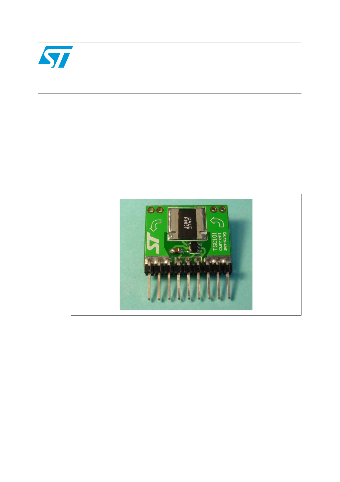
Figure 1. Demonstration board
June 2008 Rev 1 1/6
www.st.com
Page 2
About the TSC101 AN2727
1 About the TSC101
The TSC101 measures a very small voltage drop on a high-side shunt resistor, and, using
an internally fixed gain, amplifies the dif ference into a ground-ref erenced o utput volt age. The
amplification gain is internally fixed and the device is housed in a tiny SOT23-5 package.
Input common-mode and power supply voltages are independent. The common-mode
voltage can range fr om 2.8 V to 30 V in operating conditions , and up to 60 V in absolute
maximum ratings. The supply voltage can range from 4 V to 24 V giving you the possibility
to connect the power supply pin to either side of the shunt resistor in most cases.
Most of the TSC101 parameters are guar anteed over the fu ll operating temperature range
from -40° C to 125° C.
Current consumption of less than 300 µA over the temperature range and low input bias
current (less than 8 µA in standard conditions, a few 100 nA if V
particularly interesting to save power in the application.
The TSC101 key features are:
● Independent supply and input common-mode voltages
● Wide common-mode operating range: 2.8 V to 30 V
● Wide common-mode surviving range: -0.3 V to 60 V (load-dump)
● Wide supply voltage range: 4 V to 24 V
● Low current consumption: I
● Internally fixed gain: 20 V/V (TSC101A), 50 V/V (TSC101B) or 100 V/V (TSC101C)
● Buffered output
max is 300 µA
CC
isn’t supplied) are
CC
For more detailed information about the TSC101, refer to the datasheet.
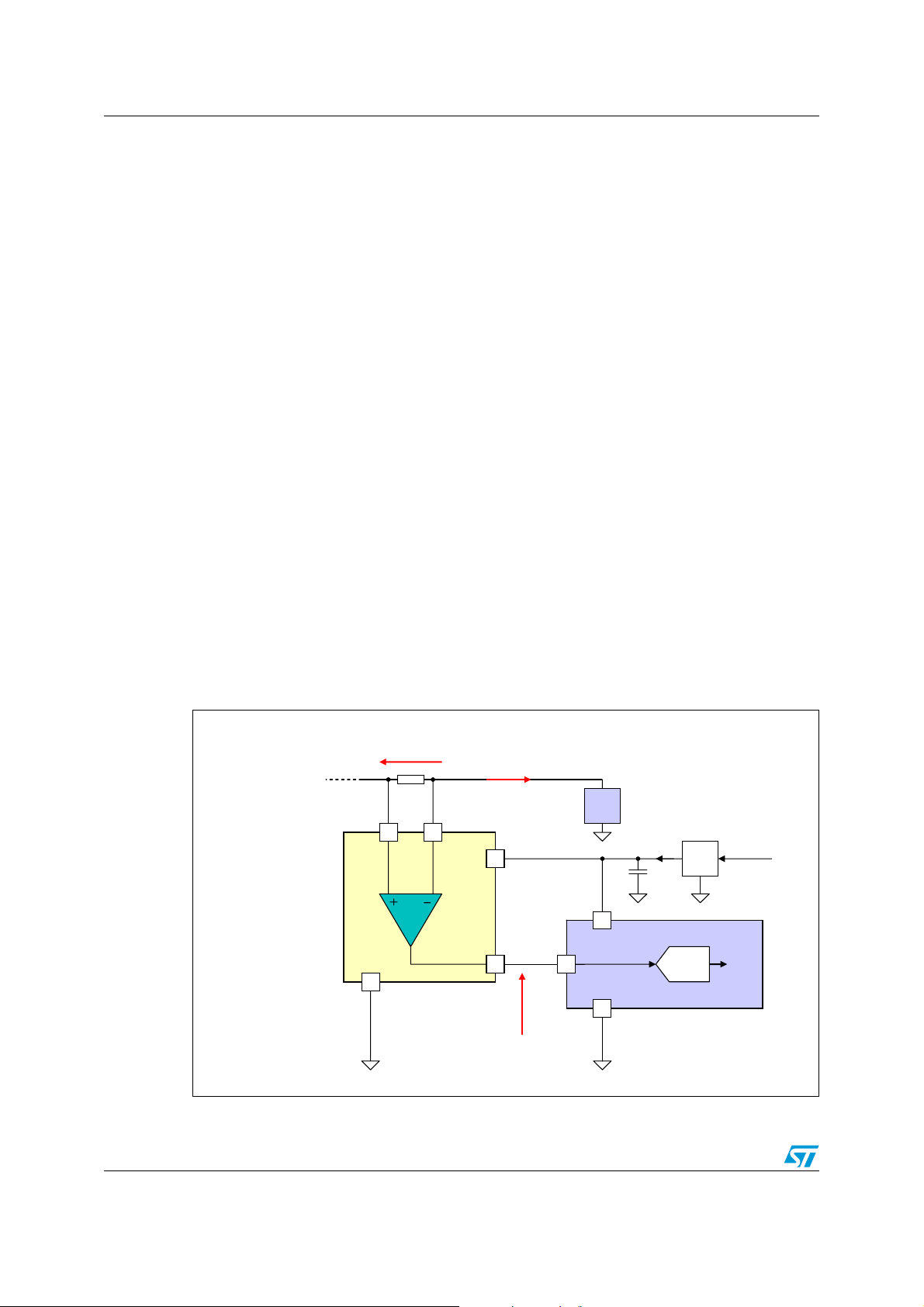
Figure 2. Typical application for the TSC101
V
battery or power
source
2.8V to 30V
Vp Vm
Gnd
sense
R
sense
43
2
TSC101
Current Sensing
Amplifier
Vcc
Out
I
load
load
5V
5
V
CC
1
V
out
Gnd
Microcontroller
ADC
V
reg
2/6
Page 3

AN2727 Description of the demonstration board
2 Description of the demonstration board
The DEMO_TSC101 is a demonstration board designed to help you evaluate the
performance of the TSC101.
Figure 3. Demonstration board schematic diagram
J2
1
Current_in
R1
1 2
3
4
R2
J3
1
Current_out
TSC101
VCC
OUT
IC1
5
C1
CAP
J1
1
1
2
3
CON3
3
VP VM
J4
1
Gnd
Table 1. Demonstration board bill of materials
2
4
GND
Part Part type Footprint Description Manufacturer Reference
IC1 TSC101B SOT23-5
R1 WSL3637
9.4mm x
9.14mm
High-side current sensing
amplifier
STMicroelectronics TSC101BILT
5mΩ shunt resistor Vishay Dale
C1 100nF/X7R 0402
Supply voltage decoupling
capacitor
3/6
Page 4

Demonstration board layout AN2727
3 Demonstration board layout
The printed circuit board of the demonstration board has the following characteristics:
● Board dimensions: 23 mm x 18 mm
● 2-layer PCB
● PCB thickness: 0.8 mm
● FR4 material
● Copper thickness: 18 µm
Figure 4. Top view of demonstration board
Figure 5. Bottom view of demonstration board
4/6
Page 5

AN2727 Revision history
4 Revision history
Table 2. Document revision history
Date Revision Changes
3-Jun-2008 1 First release.
5/6
Page 6

AN2727
Please Read Carefully:
Information in this document is provided solely in connection with ST products. STMicroelectronics NV and its subsidiaries (“ST”) reserve the
right to make changes, corrections, modifications or improvements, to this document, and the products and services described herein at any
time, without notice.
All ST products are sold pursuant to ST’s terms and conditions of sal e.
Purchasers are solely res ponsibl e fo r the c hoic e, se lecti on an d use o f the S T prod ucts and s ervi ces d escr ibed he rein , and ST as sumes no
liability whatsoever relati ng to the choice, selection or use of the ST products and services de scribed herein.
No license, express or implied, by estoppel or otherwise, to any intellectual property rights is granted under this document. If any part of this
document refers to any third pa rty p ro duc ts or se rv ices it sh all n ot be deem ed a lice ns e gr ant by ST fo r t he use of su ch thi r d party products
or services, or any intellectua l property c ontained the rein or consi dered as a warr anty coverin g the use in any manner whats oever of suc h
third party products or servi ces or any intellectual property contained therein.
UNLESS OTHERWISE SET FORTH IN ST’S TERMS AND CONDITIONS OF SALE ST DISCLAIMS ANY EXPRESS OR IMPLIED
WARRANTY WITH RESPECT TO THE USE AND/OR SALE OF ST PRODUCTS INCLUDING WITHOUT LIMITATION IMPLIED
WARRANTIES OF MERCHANTABILITY, FITNESS FOR A PARTICUL AR PURPOS E (AND THEIR EQUIVALE NTS UNDER THE LAWS
OF ANY JURISDICTION), OR INFRINGEMENT OF ANY PATENT, COPYRIGHT OR OTHER INTELLECTUAL PROPERTY RIGHT.
UNLESS EXPRESSLY APPROVED IN WRITING BY AN AUTHORIZED ST REPRESENTATIVE, ST PRODUCTS ARE NOT
RECOMMENDED, AUTHORIZED OR WARRANTED FOR USE IN MILITARY, AIR CRAFT, SPACE, LIFE SAVING, OR LIFE SUSTAINING
APPLICATIONS, NOR IN PRODUCTS OR SYSTEMS WHERE FAILURE OR MALFUNCTION MAY RESULT IN PERSONAL INJ URY,
DEATH, OR SEVERE PROPERTY OR ENVIRONMENTAL DAMAGE. ST PRODUCTS WHICH ARE NOT SPECIFIED AS "AUTOMOTIVE
GRADE" MAY ONLY BE USED IN AUTOMOTIVE APPLICATIONS AT USER’S OWN RISK.
Resale of ST products with provisions different from the statements and/or technical features set forth in this document shall immediately void
any warranty granted by ST fo r the ST pro duct or serv ice describe d herein and shall not cr eate or exten d in any manne r whatsoever , any
liability of ST.
ST and the ST logo are trademarks or registered trademarks of ST in various countries.
Information in this document su persedes and replaces all info rmation previously supplied .
The ST logo is a registered trademark of STMicroelectronics. All other names are the property of their respective owners.
© 2008 STMicroelectronics - All rights reserved
STMicroelectronics group of compan ie s
Australia - Belgium - Brazil - Canada - China - Czech Republic - Finland - France - Germany - Hong Kong - India - Israel - Italy - Japan -
Malaysia - Malta - Morocco - Singapore - Spain - Sweden - Switzerland - United Kingdom - United States of America
www.st.com
6/6
 Loading...