

STw4102 single Li-Ion cell battery charger including gas gauge
1 Introduction
This application note describes the STEVAL-ISB006V1, an evaluation board specifically
designed for the STw4102 battery management integrated circuit.
This document provides:
● a brief description of the STw4102
● a description of the evaluation board
● a detailed bill of materials of the evaluation board
● the layout of the evaluation board.
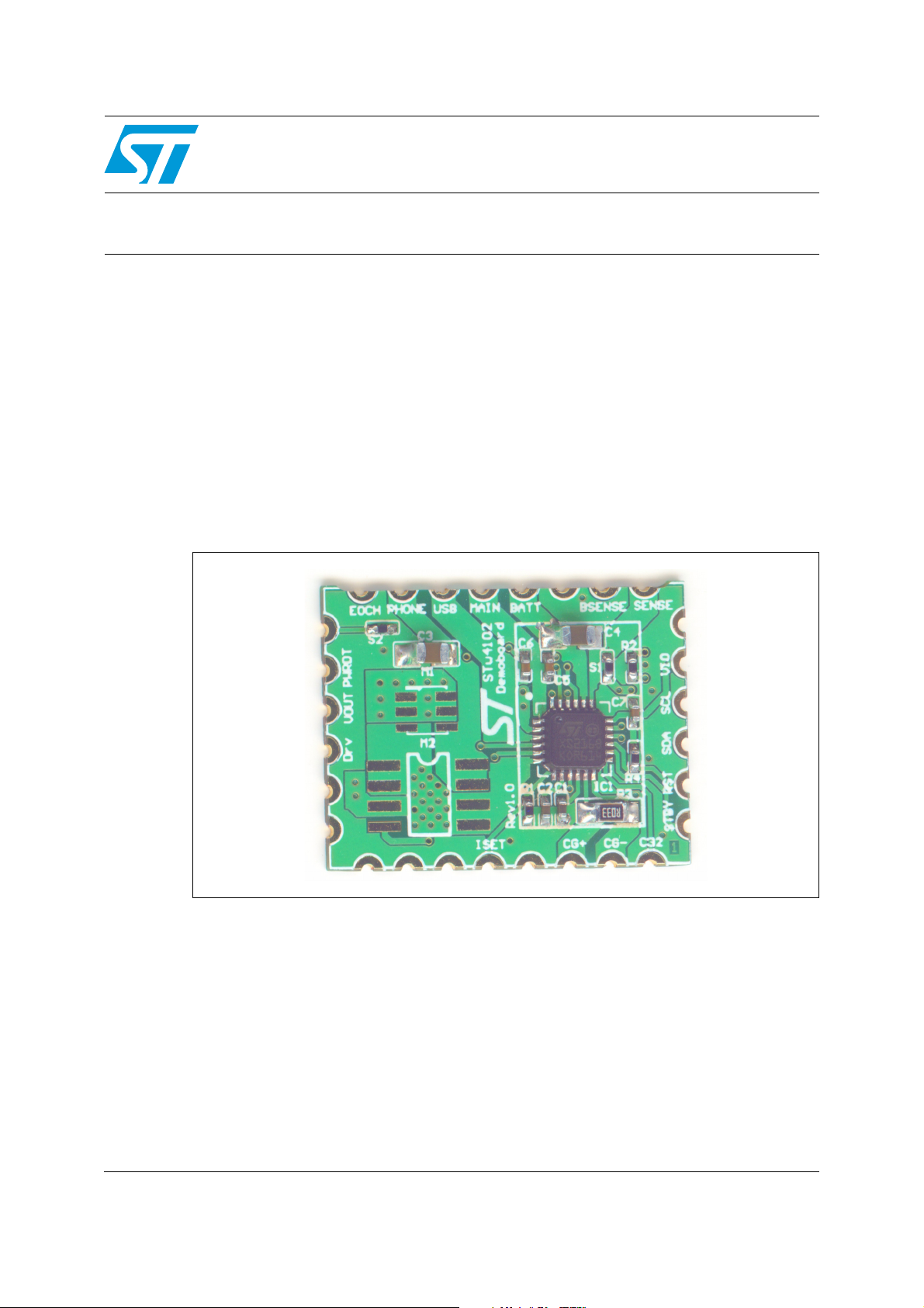
Figure 1. STw4102 evaluation board
AN2726
Application note
Evaluation board user guidelines for the
July 2008 Rev 1 1/10
www.st.com

About the STw4102 AN2726
2 About the STw4102
The STw4102 is a standalone constant-current, constant-voltage (CCCV) linear charger
dedicated to Li-Ion batteries. The device has a dual charging capability that uses the main
input adaptor (wall or car adapter) or a USB cable with no external component.
The STw4102 offers a programmable fast-charge current using an external resistor. The
thermal regulation circuitry limits the charge current so that the die junction temperature
never exceeds the maximum specified value. An end-of-charge output pin indicates the
charge termination when the fast charge current drops below 10% of the programmed
current value.The STw4102 contains an accurate gas-gauge based on a 13-bit AD
converter. An external resistor is used between the battery and ground pin to sense a
charge/discharge current. With a typical 30 mΩ resistor, the current can be up to 2.5 A and
the 24-bit accumulator system provides a capacity of up to 914 mA.h.
The STw4102 has the following key features.
■ Constant-current constant-voltage (CCCV) linear charger.
■ Common or separate USB/wall adapter inputs.
■ Fast-charge current control up to 1 A for wall adapters and up to 500 mA for USB.
■ Support for currents higher than 1 A using external components.
■ Programmable charge voltage (4.1 V, 4.2 V, 4.3 V, 4.35 V) with 1% accuracy.
■ Thermal regulation.
■ Trickle-charge mode at low battery voltage.
■ Wall adapter voltage up to 13 V.
■ Battery over-voltage protection at 4.7 V.
■ Gas gauge with 13-bit AD converter.
■ Battery voltage monitor with 7- to 12-bit AD converter.
■ I²C interface for device monitoring and control.
■ Charge status output pin.
■ Power detection output pin.
■ Programmable watchdog security timer.
■ 4.7 V LDO regulator (with external power MOSFET).
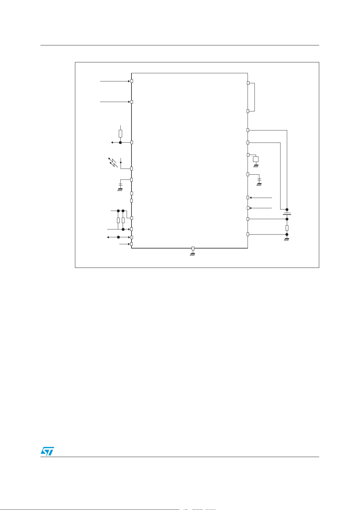
Figure 2 describes the application schematics, with the typical connections and peripheral
components surrounding the charger IC.
2/10
AN2726 About the STw4102
Figure 2. Typical application for the STw4102
TO$""
)NDICATOR,%$
2ESET
)/VOLTAGE
#
)/VOLTAGE
-!).
53"072
072$%4%#4.
%/#('
#62%&
,$/$26
,$/&"
6)/
3#,
3$!
2%3%4.
34W
'.$
6/54
3%.3%
"!44
"!443%.3%
)3%4
#6)3
#+(:
34$"9
)#'
)#'
2
#
K(Z
3TAND"Y
2
Refer to the datasheet for more detailed information on the STw4102.
3/10

Description of the demonstration board AN2726
3 Description of the demonstration board
The STEVAL-ISB006V1 is a demonstration board designed to help you evaluate the
performances of the STw4102.
This section explains how to evaluate the battery charger and the current gauge in a typical
application configuration.
Figure 3. Demonstration board schematic diagram
MAIN
1
M2B
STS2DPFS20V
M2A
STS2DPFS20V
PHONE
1
22uF/6.3V/X5R
DRV
1
C5
100nF/16V/X7R
USB
1
PWRDT
1
EOCH
1
VIO
1
100nF/16V/X7R
SCL
1
SDA
1
RST
1
C3
M1
STT4PF20V
100nF/16V/X7R
Vbat
1uF/6.3V/X5R
C7
C6
R2
10K
C2
R4
10K
GND
IC1
1
MAIN
3
USBPWR
24
PWRDETECTN
22
EOCHG
8
CVREF
5
LDODRV
6
LDOFB
18
VIO
17
SCL
16
SDA
15
RESETN
Epad
1
4
Driver
BATTSENSE
STw4102
GND9TEST
23
1
VOUT
SENSE
BATT
CV IS
C32kHz
STDBY
ICG+
S2
0R
TEST
ISET
ICG-
2
S1
0R
19
20
21
7
10
C1
1uF/6.3V/X5R
13
14
11
12
Vbat
R1
12K +/-1%
R3
R033 +/-1% 0805
1
VOUT
1
SENSE
BATT
1
1
BSENSE
1
ISET
1
C32
1
STBY
1
CG+
1
CG-
C4
22uF/6.3V/X5R
1
GNDBATT
4/10

AN2726 Description of the demonstration board
Table 1. Evaluation board bill of materials
Component Part type Footprint Description Manufacturer Reference
IC1 STw4102 QFN24
C1 1µF/6.3V/X5R 0402
C2 1µF/6.3V/X5R 0402
C3 22µF/6.3V/X5R 0805
Dual-source Li-Ion charger
with gas gauge
Internal supply decoupling
capacitor
Voltage reference decoupling
capacitor
Phone supply decoupling
capacitor
STMicroelectronics STw4102
Taiyo Yuden JMK105BJ105KV
Taiyo Yuden JMK105BJ105KV
Taiyo Yuden JMK212BJ226KG
C4 22µF/6.3V/X5R 0805 Battery decoupling capacitor Taiyo Yuden JMK212BJ226KG
C5 100nF/16V/X7R 0402
C6 100nF/16V/X7R 0402
C7 100nF/16V/X7R 0402
Main supply decoupling
capacitor
USB supply decoupling
capacitor
Digital supply decoupling
capacitor
Taiyo Yuden EMK105BJ104KV
Taiyo Yuden EMK105BJ104KV
Taiyo Yuden EMK105BJ104KV
M1 STT4PF20V SOT23-6 External LDO P-Mosfet STMicroelectronics STT4PF20V
M2 STS2DPFS20V SO8
R1 12K ±1% 0402
External LDO P-Mosfet and
Schottky diode
Rset resistor for fast charge
current setting
STMicroelectronics STS2DPFS20V
R2 10K ±1% 0402
PWRDETECTN pull-up
resistor
R3 R033 ±1% 0805 Gas gauge shunt resistor Phycomp 235051117330
R4 10K ±1% 0402 RESETN pull-up resistor
S1 0R 0402 Strap
S2 0R 0402 Strap
Note: The M1 and M2 components (two external P-Mosfets plus a Schottky diode) are not
mounted on the standard configuration of the demoboard. They can be added at a later
stage to test the external LDO feature.
5/10

Evaluation board layout AN2726
4 Evaluation board layout
The evaluation board’s printed circuit board has the following characteristics.
● Board dimensions: 22.7 mm x 17 mm.
STw4102 and peripheral components PCB area: 12.4 mm x 7.5 mm (0.93 cm
0.14 inch
● 4-layer PCB, FR4 material
● PCB thickness: 0.8 mm, copper thickness: 18 µm
2
):
These standards are similar to the ones used by portable equipment manufacturers.
Figure 4. Demonstration board (top view)
2
or
Figure 5. Demonstration board (bottom view)
6/10

AN2726 Evaluation board layout
Figure 6. Internal layers of the demonstration board
Figure 7. Single-connector application typical schematic
Power Detected
System
Controller
(if R1 removed)
Vio
Gnd
Charging
VBUS
Gnd
| Battery +
7/10

Evaluation board layout AN2726
Figure 8. Dual-connector application typical schematic
Power Detected
Charging
System
Controller
(if R1 removed)
Vio
Gnd
VBUS
Gnd
Vdc
Adapter
(5V DC)
Gnd
| Battery +
8/10

AN2726 Revision history
5 Revision history
Table 2. Document revision history
Date Revision Changes
10-Jul-2008 1 Initial release.
9/10

AN2726
Please Read Carefully:
Information in this document is provided solely in connection with ST products. STMicroelectronics NV and its subsidiaries (“ST”) reserve the
right to make changes, corrections, modifications or improvements, to this document, and the products and services described herein at any
time, without notice.
All ST products are sold pursuant to ST’s terms and conditions of sale.
Purchasers are solely responsible for the choice, selection and use of the ST products and services described herein, and ST assumes no
liability whatsoever relating to the choice, selection or use of the ST products and services described herein.
No license, express or implied, by estoppel or otherwise, to any intellectual property rights is granted under this document. If any part of this
document refers to any third party products or services it shall not be deemed a license grant by ST for the use of such third party products
or services, or any intellectual property contained therein or considered as a warranty covering the use in any manner whatsoever of such
third party products or services or any intellectual property contained therein.
UNLESS OTHERWISE SET FORTH IN ST’S TERMS AND CONDITIONS OF SALE ST DISCLAIMS ANY EXPRESS OR IMPLIED
WARRANTY WITH RESPECT TO THE USE AND/OR SALE OF ST PRODUCTS INCLUDING WITHOUT LIMITATION IMPLIED
WARRANTIES OF MERCHANTABILITY, FITNESS FOR A PARTICULAR PURPOSE (AND THEIR EQUIVALENTS UNDER THE LAWS
OF ANY JURISDICTION), OR INFRINGEMENT OF ANY PATENT, COPYRIGHT OR OTHER INTELLECTUAL PROPERTY RIGHT.
UNLESS EXPRESSLY APPROVED IN WRITING BY AN AUTHORIZED ST REPRESENTATIVE, ST PRODUCTS ARE NOT
RECOMMENDED, AUTHORIZED OR WARRANTED FOR USE IN MILITARY, AIR CRAFT, SPACE, LIFE SAVING, OR LIFE SUSTAINING
APPLICATIONS, NOR IN PRODUCTS OR SYSTEMS WHERE FAILURE OR MALFUNCTION MAY RESULT IN PERSONAL INJURY,
DEATH, OR SEVERE PROPERTY OR ENVIRONMENTAL DAMAGE. ST PRODUCTS WHICH ARE NOT SPECIFIED AS "AUTOMOTIVE
GRADE" MAY ONLY BE USED IN AUTOMOTIVE APPLICATIONS AT USER’S OWN RISK.
Resale of ST products with provisions different from the statements and/or technical features set forth in this document shall immediately void
any warranty granted by ST for the ST product or service described herein and shall not create or extend in any manner whatsoever, any
liability of ST.
ST and the ST logo are trademarks or registered trademarks of ST in various countries.
Information in this document supersedes and replaces all information previously supplied.
The ST logo is a registered trademark of STMicroelectronics. All other names are the property of their respective owners.
© 2008 STMicroelectronics - All rights reserved
STMicroelectronics group of companies
Australia - Belgium - Brazil - Canada - China - Czech Republic - Finland - France - Germany - Hong Kong - India - Israel - Italy - Japan -
Malaysia - Malta - Morocco - Singapore - Spain - Sweden - Switzerland - United Kingdom - United States of America
www.st.com
10/10
 Loading...