

Page 1
AN2722
Application note
Demonstration board user guidelines for the
TS4601B high-performance stereo headphone driver
Introduction
This application note concerns the TS4601B’s demonstration board, designed to evaluate
the TS4601B, a high-performance stereo headphone driver with capacitor-less outputs and
2
I
C interface from STMicroelectronics.
This document provides:
■ a brief description of the TS4601B device.
■ a description of the demonstration board and all of its components.
■ a description of the TS4601B control software provided.
■ the layout of the demonstration board.
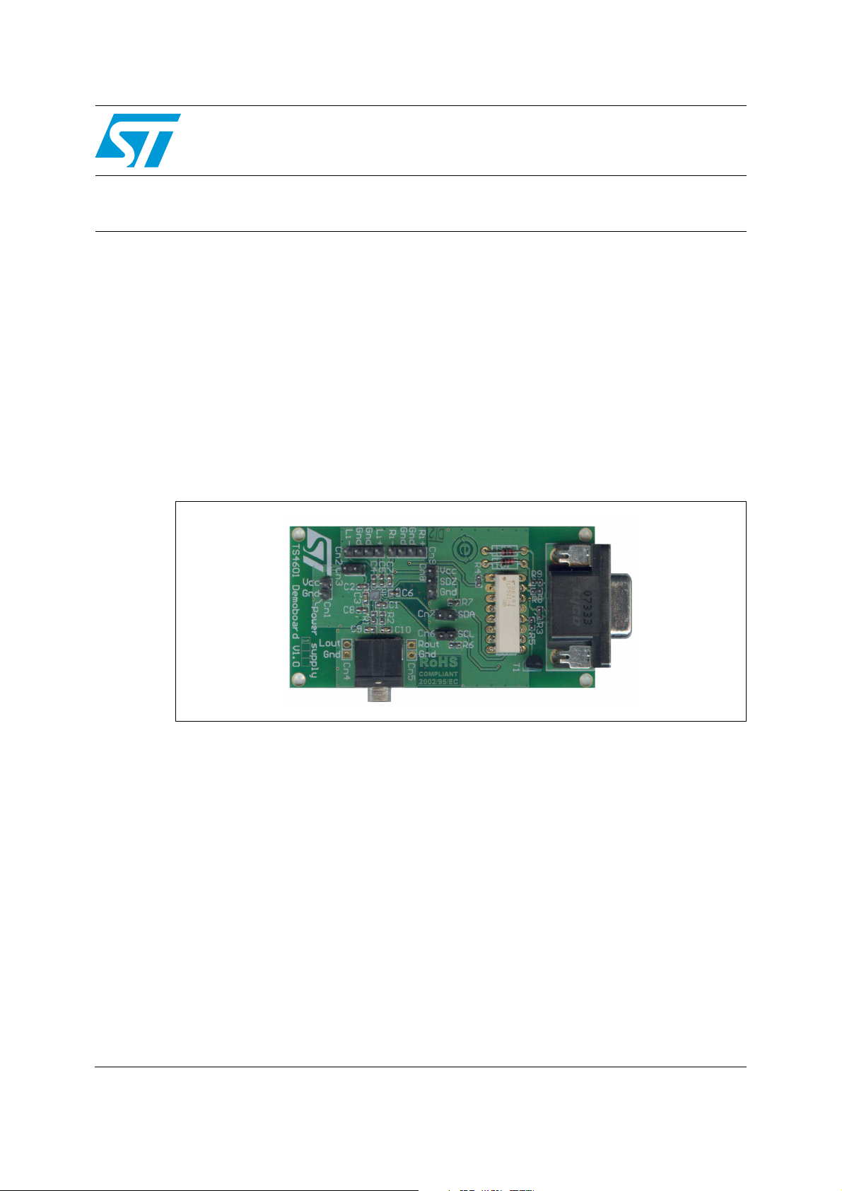
Figure 1. TS4601B demonstration board
About the TS4601B
The TS4601B is a stereo headphone driver dedicated to high audio performance and
space-constrained applications. It is based on a low-power dissipation amplifier core
technology. Special care was taken in the design of the amplification chain to achieve
peerless PSRR (107 dB typ. at 217 Hz) and 101 dB of SNR.
The TS4601B can drive at minimum 0.9 V
10 kΩ, regardless of the power supply voltage, in the range of 2.9 to 5.5 V.
An I²C interface is used to control the volume through 64 steps ranging from -60 dB to +4 dB
and to configure the device in multiple modes. The traditionally-used output-coupling
capacitors can be removed and a dedicated common-mode sense pin suppresses parasitic
noise from the jack.
The TS4601B is designed to be used with an output serial resistor. It ensures unconditional
stability over a wide range of capacitive loads. It is packaged in a tiny 16-bump flip chip
package with a pitch of 500 µm and a 300-µm diameter ball size.
March 2009 Rev 2 1/16
output voltage into 16 Ω and 1.6 V
rms
rms
into
www.st.com
Page 2

The TS4601B has the following key features.
■ Power supply range: 2.9 to 5.5 V
■ 107 dB of PSRR at 217 Hz
■ Fully-differential inputs
■ I²C interface for volume control
■ Digital volume control range from -60 dB to +4 dB
■ 101 dB of SNR A-weighted
■ Independent right and left channel shutdown control
■ Low quiescent current: 4.8 mA typ. at 3.0 V
■ Low standby current: 2 µA max
■ Output coupling capacitors removed
■ Flip-chip package: 2.1 mm x 2.1 mm, 500 µm pitch, 16 bumps
Refer to the datasheet for complete information on the TS4601B.
AN2722
2/16
Page 3
AN2722 Description of the demonstration board
1 Description of the demonstration board
The TS4601B demonstration board is designed to help you evaluate the TS4601B audio
differential input stereo headphone amplifier. The TS4601B device, in a flip chip package, is
mounted on a four-layer PCB. An on-board RS-232 to I
to control from a personal computer by using its serial port.
The provided software controls all of the TS4601B’s features (gain, mode, mute, standby
and register status).
You can use the connectors on the demonstration board to directly control some of the
features.
● The master standby of the TS4601B can be set directly by Cn8 or, if the jumper is
removed, by an external digital control (see Ta bl e 1 ).
● By removing the jumpers on Cn6 and Cn7, you can disconnect the on-board I
interface so that you can control the TS4601B by an external I
● The -3 dB cut-off input high-pass filter is set at about 6 Hz (C4 to C7). If you want to
change this frequency, you have to replace C4 to C7 at the same time. More
information about these component calculations is available in the TS4601B datasheet.
● The actual current consumption of the TS4601B can be measured directly by removing
the jumper on Cn3 and inserting a DC amperemeter in series. The overall current
consumption of the demonstration board is higher than the consumption of the
TS4601B because the Cn1 power supply connector supplies the RS-232 to I
in addition to the TS4601B.
Table 1. Demonstration board connectors
2
C interface makes this board easy
2
2
C bus interface.
C
2
C adapter
Connector Description
Cn1 Power connector (V
Fully-differential positive and negative input signal connectors (active input signal
Cn2, Cn9
Cn3
Cn4 Left output connector (GND and active signal).
Cn5 Right output connector (GND and active signal).
Cn6, Cn7
Cn8
and GND). By shorting one active input to GND, you can use the demonstration
board in single-ended input mode (refer to the TS4601B datasheet for more
information).
Connector that allows direct measurement of TS4601B’s current consumption.
Remove the jumper and insert a DC amperemeter.
SCL and SDA connectors:
– pins shorted, TS4601B is controlled by the on-board RS 232 to I
– pins unshorted, TS4601B can be controlled by an external I
Standby control connector:
– when pins 1 and 2 are shorted, the TS4601B is in operation mode.
– when pins 2 and 3 are shorted, the TS4601B is in master standby mode.
The connector pins are connected as follows:
– pin 1 to V
– pin 2 to SDZ of the TS4601B
– pin 3 to GND
CC
and GND). Power supply voltage from 2.9 V to 5.5 V.
CC
2
C bus.
2
C interface.
3/16
Page 4

Description of the demonstration board AN2722
Table 1. Demonstration board connectors (continued)
Connector Description
J1 3.5 mm stereo headphone plug.
J2
DB9 female connector enabling connection of the demonstration board to the
RS-232 serial port.
Caution: When you apply the power supply through Cn1, do not invert the polarity as this will
damage the U1 amplifier.
4/16
Page 5
AN2722 Description of the demonstration board
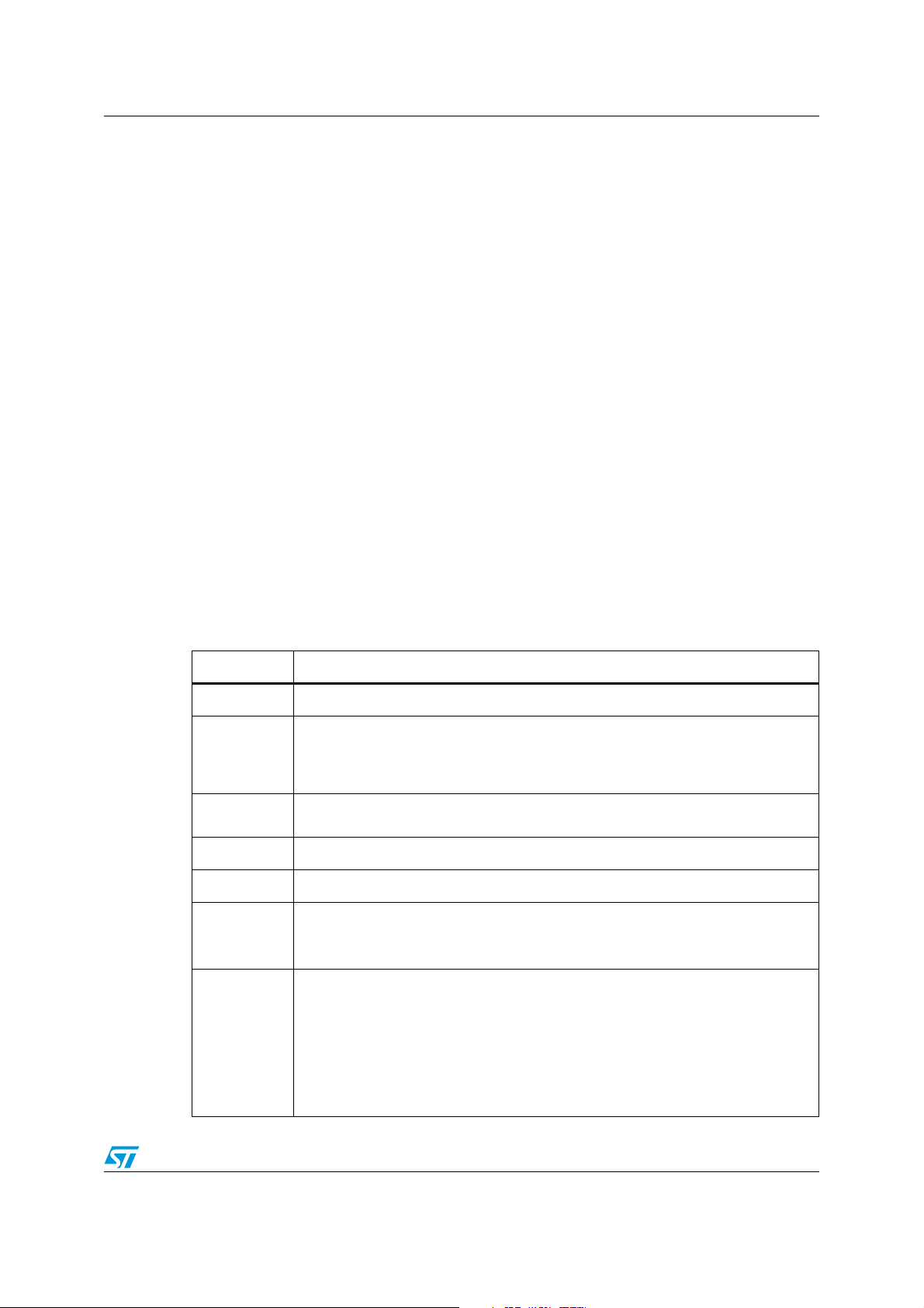
Figure 2. Schematic diagram
VccI2C Vcc
Cn8
Stdby
Vcc
1
2
3
GndP
Cn1
Power
Cn2
Cn9
GndP
Left Input
Right Input
Gnd
Gnd
Cn3
C4
2.2uF
C5
2.2uF
SDA
SCL
C6
2.2uF
C7
2.2uF
Gnd
B4
B3
D4
C3
C4
D3
D2
GndP
TS4601
InL-
InL+
SDZ
InR+
InR-
SDA
I2C
SCL
PVcc Gnd C1 C2
Vcc
-
+
+
-
Negative
Supply
A4 A3 A2 A1
C2
C3
1uF
1uF
GndP GndPGndP
Cn6
SCL SDA
C1
1uF
C1
Gnd
Vcc
Positive
-
+
+
-
Negative
PVss
Reg
Reg
VoutL
CMS
VoutR
U1
Gnd
Gnd
C9
2.2nF
R1
B1
12
C2
R2
D1
12
C10
2.2nF
Gnd
Cn4
Left Output
J1
1
2
3
Gnd
Cn5
Right Output
Gnd
B2
C8
Cn7
2.2uF
Vcc
TS4601 main application
J2
DB9
5
9
4
8
3
7
2
6
1
GND
DTR
TXD
RTS
DSR
SCL
VccI2C
R4
180
U2A
16
15
KP1040
R3
1K
R8
2k2
R9
1K
D1
1N4148
D2
1N4148
1
T1
BS170
U2B
KP1040
U2C
KP1040
R5
100
2
GndP GndPGND2
3
4
GND2
5
6
GND2
SDA
14
13
GndP
12
11
GndP
R6
10KR710K
RS232 to I2C converter
5/16
Page 6

Description of the demonstration board AN2722
Table 2. Component list for the demonstration board
Name Quantity Description
C1, C2, C3 3 1 µF/10V X5R, SMD ceramic capacitors, 0603
C4, C5, C6, C7,
C8
C9, C10 2 2.2 nF/50V X7R, SMD ceramic capacitors, 0603
Cn1, Cn3, Cn4,
Cn5, Cn6, Cn7
Cn8 1 3-pin header 2.54 mm pitch
Cn2, Cn9 2 4-pin header 2.54 mm pitch
D1, D2 2 1N4148,
J1 1 3.5 mm stereo PCB headphone jack connector
J2 1 PCB 90° female DB9 connector
R1, R2 2 12 Ω/1% SMD resistor, 0603
R3, R9 2 1 kΩ/1% SMD resistor, 0603
R4 1 180 Ω/1% SMD resistor, 0603
5 2.2 µF/10V X5R, SMD ceramic capacitors 0603
6 2-pin header 2.54 mm pitch
R5 1 100 Ω/1% SMD resistor, 0603
R6, R7 2 10 kΩ/1% SMD resistor, 0603
R8 1 2.2 kΩ/1% SMD resistor, 0603
T1 1 BS170
U1 1 TS4601BEIJ
U2 1 KP1040, TLP521-4(GB)
6/16
Page 7

AN2722 Demonstration board layout
2 Demonstration board layout
The following figures show the layers and the top view of the demonstration board.
Figure 3. PCB top layer PCB mid layer 1
Figure 4. PCB mid layer 2 PCB bottom layer
7/16
Page 8

Demonstration board layout AN2722
Figure 5. Top view of the demonstration board
8/16
Page 9

AN2722 TS4601B demonstration software
3 TS4601B demonstration software
The TS4601B demonstration software provides a quick and easy way of driving the
TS4601B audio system from a PC, and in particular, of configuring the output mode and the
volume.
The software is located on the CDROM provided with the demonstration board. The latest
revision of this software is available on the ST web site at www.st.com. It runs under MS
Windows 95/98/ME/2000/XP.
The PC must have a serial port available. If not, a USB-to-serial adapter can be used but
note that the compatibility with all adapters available on the market has not been tested.
3.1 Connecting the demonstration board and starting the software
Follow these steps to drive the TS4601B from a PC.
1. Use a DB9 female to DB9 male RS-232 cable to connect the PC to the TS4601B
demonstration board on J2.
2. Connect the power supply V
pin 2.
3. Verify that Cn3, Cn6 and Cn7 are shorted.
4. Connect the modulation source to Cn2 and Cn3, and plug a headphone into J1.
5. Copy the TS4601B demonstration board program board.exe provided on the
CDROM onto the hard drive of your PC and launch it by double-clicking on it (no
installation needed, you can just copy it).
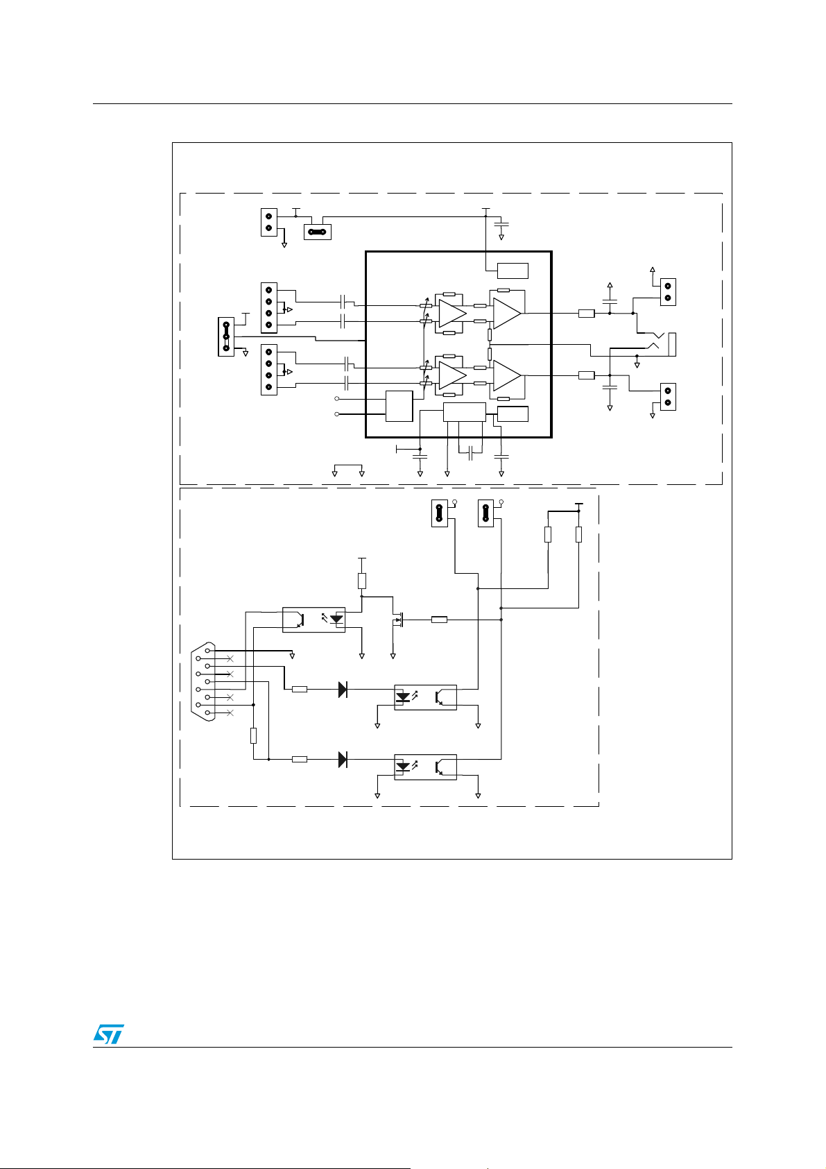
The software dialog box shown in Figure 6 is displayed.
to Cn1, and set the jumper on Cn8 to short pin 1 and
CC
9/16
Page 10
TS4601B demonstration software AN2722
g
g
Figure 6. TS4601B demonstration software main window
Read internal
isters menu
re
Internal TS4601
diagram:
changes when
Output Mode
buttons
Mute buttons
output mode
es
chan
Actual volume
indicator
Volume control
cursor
Serial Port selection
Software exit
button
6. Choose the appropriate COM port from the Port area or click Auto Detect for the
program to select the COM port automatically.
When the Port Status indicator turns to green, the program is ready to send
commands to the TS4601B.
In some rare cases, when auto detect is used, a COM port is chosen (Port Status is
green) but it is not the right one. If this happens, manually force the right COM port by
clicking directly into the Port box.
Note: The COM port where the device is connected must be in the range of COM1 to COM8. If
this is not the case, change the COM port number in Windows by selecting Start>Control
Panel>System>Hardware>Device Manager.
3.2 Using the TS4601B software
In the main window of the TS4601B demonstration software shown in Figure 6, on the left
side the following features are available.
● Mode select buttons
Allow you to select the TS4601B output mode. The diagram located in the middle of the
window summarizes the mode currently selected and shows which inputs and outputs
are active. The indicator located to the right of each output mode lights up when the
mode is active. Figure 7 shows an example of this window when the software is in
operation.
10/16
Page 11

AN2722 TS4601B demonstration software
Figure 7. TS4601B main window in operating mode
● Mute buttons
Allow you to set the TS4601B output to mute or operating mode. When the indicator
located to the right lights up in green, the channel mute is active.
● Read internal register menu
When you click on this menu, the TS4601B Internal Registers pop-up window is
displayed (see Figure 8). By clicking on the Read Internal Registers button, you can
display the actual state of the TS4601B. Hexadecimal values of CR0 to CR4 registers
are also displayed. By pressing the Clear Results button, all results disappear and you
need to press again the Read Internal Registers button for a new display.
Note that this window remains open until you close it by clicking on the cross in the
upper right corner.
Note also that this window is not automatically refreshed. If you change the output
mode or something else in the main window, you have to press again the Read
Internal Registers button to display the new TS4601B settings.
11/16
Page 12

TS4601B demonstration software AN2722
Figure 8. TS4601B main window + register status window
In the main window of the TS4601B evaluation software shown in Figure 6, on the right side
the following feature is available.
● Volume control cursor
By dragging this cursor up and down, you can control the TS4601B’s output volume.
The actual gain set is displayed in the Gain box.
To exit the program, just click the Exit button on the bottom right or click the cross in the
upper right corner of the window.
Note: Occasionally, problems may arise when trying to drive the demonstration board using
certain notebook or laptop PCs and the RS-232 output.
12/16
Page 13

AN2722 TS4601B demonstration software
3.3 Common error messages
No acknowledge for address
You pressed an output mode button and the software displays an information pop-up
window that indicates “Error: No acknowledge for address!” (see example in Figure 9).
This error message can have several causes.
● You set the device in master standby mode. Either Cn8 between 2 and 3 or the SDZ pin
were left floating.
● The power supply is down or disconnected from Cn1.
● One or several jumpers are missing on Cn6 or Cn7.
● The serial cable is disconnected from J2.
● The jumper on Cn3 is missing and there is no amperemeter in series.
Figure 9. TS4601B acknowledge pop-up message
Results displayed in Internal Registers window are different from main window
You pressed the read internal registers button in the TS4601B internal registers window,
and results displayed are different from what the main window indicates (see Figure 10).
The main window is not automatically refreshed, therefore, this case can appear if, while the
software is running, you switch the TS4601B power supply OFF and ON or set the TS4601B
to master standby (by setting the pin SDZ to "0") and set it back again to I
2
C standby (SDZ
to level "1"). When you do this, the TS4601B is reset and all internal registers are set to their
initial value. This is why, when you press the Read Internal Registers button, the result
displayed is quite different from the display in the main window.
Pressing again one of the output mode buttons or just changing the volume is enough to restart the TS4601B without closing and re-starting the software.
13/16
Page 14

TS4601B demonstration software AN2722
Figure 10. Uncorrelated windows in TS4601B evaluation software
14/16
Page 15

AN2722 Revision history
4 Revision history
Table 3. Document revision history
Date Revision Changes
17-Apr-2008 1 Initial release.
13-Mar-2009 2
Minor text changes.
Changed part number from TS4601 to TS4601B.
15/16
Page 16

AN2722
Please Read Carefully:
Information in this document is provided solely in connection with ST products. STMicroelectronics NV and its subsidiaries (“ST”) reserve the
right to make changes, corrections, modifications or improvements, to this document, and the products and services described herein at any
time, without notice.
All ST products are sold pursuant to ST’s terms and conditions of sale.
Purchasers are solely responsible for the choice, selection and use of the ST products and services described herein, and ST assumes no
liability whatsoever relating to the choice, selection or use of the ST products and services described herein.
No license, express or implied, by estoppel or otherwise, to any intellectual property rights is granted under this document. If any part of this
document refers to any third party products or services it shall not be deemed a license grant by ST for the use of such third party products
or services, or any intellectual property contained therein or considered as a warranty covering the use in any manner whatsoever of such
third party products or services or any intellectual property contained therein.
UNLESS OTHERWISE SET FORTH IN ST’S TERMS AND CONDITIONS OF SALE ST DISCLAIMS ANY EXPRESS OR IMPLIED
WARRANTY WITH RESPECT TO THE USE AND/OR SALE OF ST PRODUCTS INCLUDING WITHOUT LIMITATION IMPLIED
WARRANTIES OF MERCHANTABILITY, FITNESS FOR A PARTICULAR PURPOSE (AND THEIR EQUIVALENTS UNDER THE LAWS
OF ANY JURISDICTION), OR INFRINGEMENT OF ANY PATENT, COPYRIGHT OR OTHER INTELLECTUAL PROPERTY RIGHT.
UNLESS EXPRESSLY APPROVED IN WRITING BY AN AUTHORIZED ST REPRESENTATIVE, ST PRODUCTS ARE NOT
RECOMMENDED, AUTHORIZED OR WARRANTED FOR USE IN MILITARY, AIR CRAFT, SPACE, LIFE SAVING, OR LIFE SUSTAINING
APPLICATIONS, NOR IN PRODUCTS OR SYSTEMS WHERE FAILURE OR MALFUNCTION MAY RESULT IN PERSONAL INJURY,
DEATH, OR SEVERE PROPERTY OR ENVIRONMENTAL DAMAGE. ST PRODUCTS WHICH ARE NOT SPECIFIED AS "AUTOMOTIVE
GRADE" MAY ONLY BE USED IN AUTOMOTIVE APPLICATIONS AT USER’S OWN RISK.
Resale of ST products with provisions different from the statements and/or technical features set forth in this document shall immediately void
any warranty granted by ST for the ST product or service described herein and shall not create or extend in any manner whatsoever, any
liability of ST.
ST and the ST logo are trademarks or registered trademarks of ST in various countries.
Information in this document supersedes and replaces all information previously supplied.
The ST logo is a registered trademark of STMicroelectronics. All other names are the property of their respective owners.
© 2009 STMicroelectronics - All rights reserved
STMicroelectronics group of companies
Australia - Belgium - Brazil - Canada - China - Czech Republic - Finland - France - Germany - Hong Kong - India - Israel - Italy - Japan -
Malaysia - Malta - Morocco - Singapore - Spain - Sweden - Switzerland - United Kingdom - United States of America
www.st.com
16/16
 Loading...