

Page 1

STCC08 application guidelines
Introduction
The purpose of this document is to:
■ Describe the STCC08 device features
■ Give technical recommendations to:
– Implement the STCC08 in the appliance
– Achieve robust STCC08 design regarding EMI tests (IEC 61000-4-4)
AN2716
June 2010 Doc ID 14460 Rev 2 1/28
www.st.com
Page 2

Contents AN2716
Contents
1 STCC08 description . . . . . . . . . . . . . . . . . . . . . . . . . . . . . . . . . . . . . . . . . 4
1.1 Main features . . . . . . . . . . . . . . . . . . . . . . . . . . . . . . . . . . . . . . . . . . . . . . . 4
1.2 STCC08 non-insulated and insulated application diagram . . . . . . . . . . . . 5
1.3 AC switch control . . . . . . . . . . . . . . . . . . . . . . . . . . . . . . . . . . . . . . . . . . . . 6
1.4 AC switch failure mode detection . . . . . . . . . . . . . . . . . . . . . . . . . . . . . . . . 6
1.4.1 STCC08 AVF output configuration . . . . . . . . . . . . . . . . . . . . . . . . . . . . . . 6
1.4.2 AC switch state detection principle . . . . . . . . . . . . . . . . . . . . . . . . . . . . . 8
1.4.3 AC switch failures detection during normal operation . . . . . . . . . . . . . . . 9
1.5 AVF signal reading synchronization . . . . . . . . . . . . . . . . . . . . . . . . . . . . . 11
1.5.1 Detection window width definition . . . . . . . . . . . . . . . . . . . . . . . . . . . . . 11
1.5.2 AC switch state detection after IN signal removal . . . . . . . . . . . . . . . . . 13
2 STCC08 consumption . . . . . . . . . . . . . . . . . . . . . . . . . . . . . . . . . . . . . . . 14
3 Recommended component values . . . . . . . . . . . . . . . . . . . . . . . . . . . . 16
4 ZVS detection application . . . . . . . . . . . . . . . . . . . . . . . . . . . . . . . . . . . 17
5 Electromagnetic compatibility (EMC) tests . . . . . . . . . . . . . . . . . . . . . 18
5.1 Demonstration board description . . . . . . . . . . . . . . . . . . . . . . . . . . . . . . . 18
5.2 IEC 61000-4-4 burst immunity test . . . . . . . . . . . . . . . . . . . . . . . . . . . . . . 18
5.2.1 Test conditions . . . . . . . . . . . . . . . . . . . . . . . . . . . . . . . . . . . . . . . . . . . . 18
5.2.2 Demonstration board immunity test . . . . . . . . . . . . . . . . . . . . . . . . . . . . 18
5.2.3 Advice to improve the application immunity . . . . . . . . . . . . . . . . . . . . . . 19
6 Conclusion . . . . . . . . . . . . . . . . . . . . . . . . . . . . . . . . . . . . . . . . . . . . . . . . 20
References . . . . . . . . . . . . . . . . . . . . . . . . . . . . . . . . . . . . . . . . . . . . . . . . . . . . . . . . . 20
Appendix A Timing definitions . . . . . . . . . . . . . . . . . . . . . . . . . . . . . . . . . . . . . . . 21
Appendix B Demonstration board component layout. . . . . . . . . . . . . . . . . . . . . 24
Appendix C Demonstration board schematic . . . . . . . . . . . . . . . . . . . . . . . . . . . 25
2/28 Doc ID 14460 Rev 2
Page 3

AN2716 Contents
Appendix D Demonstration board circuit layout view. . . . . . . . . . . . . . . . . . . . . 26
Revision history . . . . . . . . . . . . . . . . . . . . . . . . . . . . . . . . . . . . . . . . . . . . . . . . . . . . 27
Doc ID 14460 Rev 2 3/28
Page 4
STCC08 description AN2716
1 STCC08 description
1.1 Main features
The STCC08 was designed to improve the safety of home appliances (see Reference 1.).
This new device can drive up to 10 mA I
Reference 2.) and send back to the microcontroller (MCU) a signal image of the voltage
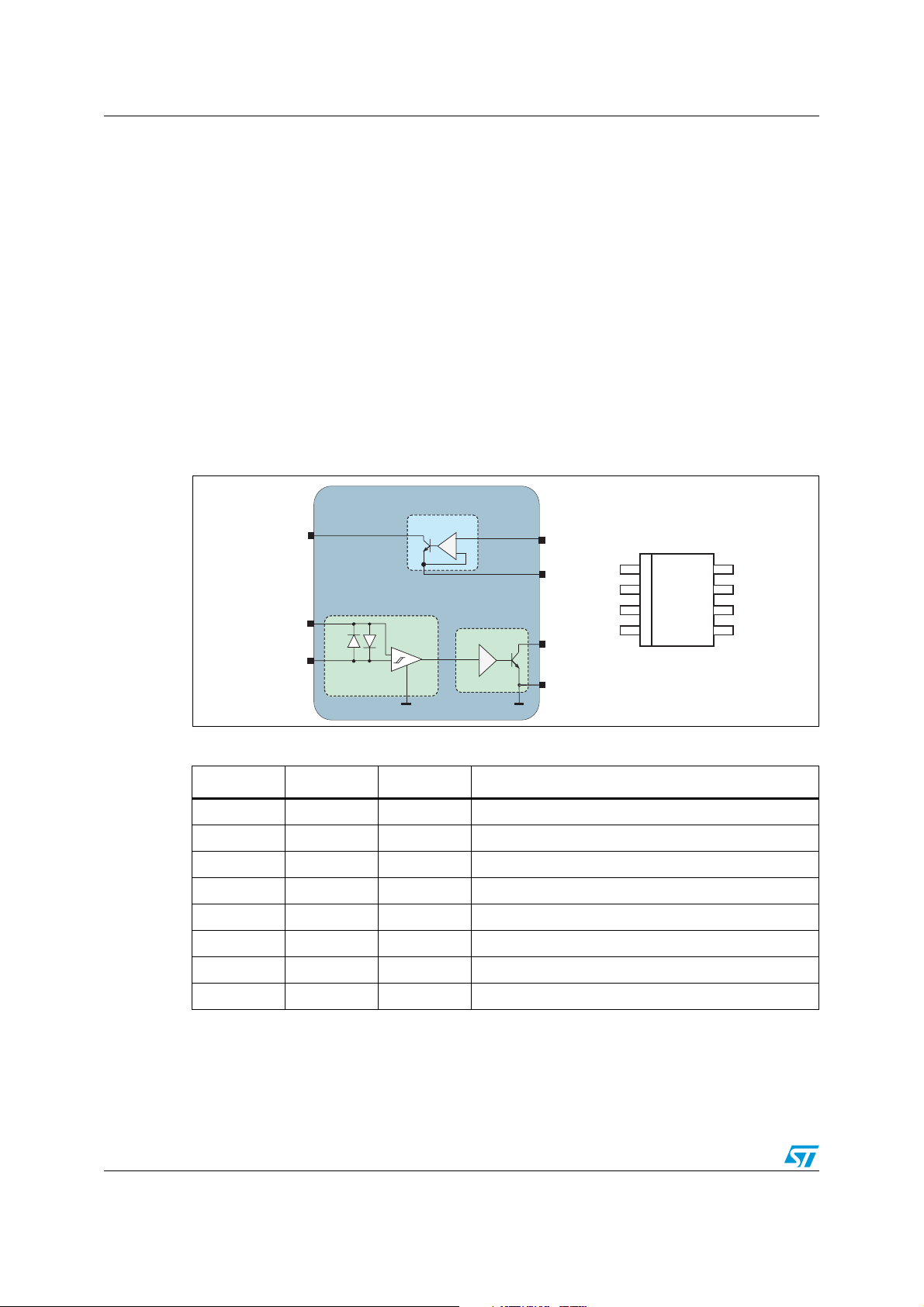
across the controlled AC switch. The STCC08 has three functional blocks (see Figure 1 and
Ta bl e 1 ).
● A “gate driver” block used to drive an AC switch and to interface directly the STCC08
with the MCU (CMOS compatible)
● A “power switch signal shaping” block used to measure the AC switch voltage
● An “AVF driver” block used to give an image of the AC switch voltage to the MCU
(digital information)
Figure 1. STCC08 block diagram
AC switches (TRIAC, ACST and ACS - see
GT
G (6)
V (5)
CC
AC (4)
Power switch
signal shaping
Table 1. STCC08 pin descriptions
Gate driver
+
-
STCC08
AVF driver
IN (1)
R (7)
IG
AVF
AVF (2)
GND
GND (8)
IN
AVF
N/C
AC
1
2
3
4
SO-8 package
Pin Symbol Type Description
1 IN SIGNAL AC switch drive
2 AVF SIGNAL Alternating voltage feedback: AC switch state output
3 NC Not connected
4 AC SIGNAL AC switch state sense input
5V
CC
POWER Positive power supply
6 G SIGNAL AC switch gate driver output
7RIGSIGNAL AC switch gate current setting
8 GND POWER Power supply reference
GND
8
R
IG
7
G
6
V
CC
5
Knowing the STCC08 IN input state (used to turn on or off the AC switch) and the voltage
across the controlled AC switch (given by the STCC08 AVF output signal state), the MCU is
able to identify all AC switch failures (diode mode, short circuit, or open circuit) and to take
the appropriate actions to put the appliance in a secure state (see Reference 3.) by
switching off an appliance front-end relay (see Section 1.4.3).
4/28 Doc ID 14460 Rev 2
Page 5

AN2716 STCC08 description
1.2 STCC08 non-insulated and insulated application diagram
The STCC08 is dedicated to applications with MCU. Figure 2 and Figure 3 show
respectively the STCC08 non-insolated and insolated application diagrams. The STCC08 is
compatible with 3.3 V and 5 V power supplies. The DC power supply must be a negative
one. This means the V
V
(3.3 V or 5 V) below neutral. Such a connection is mandatory to drive ACS and most
CC
ACST and TRIAC devices (AC switches can be triggered only by a current taken from the
gate).
Figure 2. Un-insulated application diagram
terminal has to be connected to neutral. The GND voltage is then
cc
Neutral
ACS
RAC
Load
RShunt
Line
Front end relay
G
V
CC
AC
Power switch
signal shaping
STCC08
Figure 3. Insulated application diagram
Neutral
ACS
G
Gate driver
Gate driver
+
-
+
-
AVF driver
V
CC1
IN
R
IG
VCC= 3.3V to 5V
IN
R
IG
AVF
AVF
GND
GND
Un- insulatated
5 V or 3.3 V
Power supply
R
2
IG
R
V
CC
MCU
Power supply
Insulated
V
CC
V
CC2
Line
Load
RShunt
Front end relay
RAC
V
AC
CC
Power switch
signal shaping
STCC08
STCC08
AVF driver
R
AVF
GND
OPTO1
I
G
R
1
V
CC1
R
AVF
OPTO2
V
CC2
MCU
Doc ID 14460 Rev 2 5/28
Page 6
STCC08 description AN2716
1.3 AC switch control
The STCC08 controls up to 10 mA IGTTRIAC, ACST and ACS through the “gate driver”
block designed to:
● Drive the AC switch according to the IN control input state (CMOS compatible)
– For IN = 1 = V
– For IN = 0 = GND Ö the AC switch is turned off
● Regulate the gate current of the AC switch thanks to the internal current controller
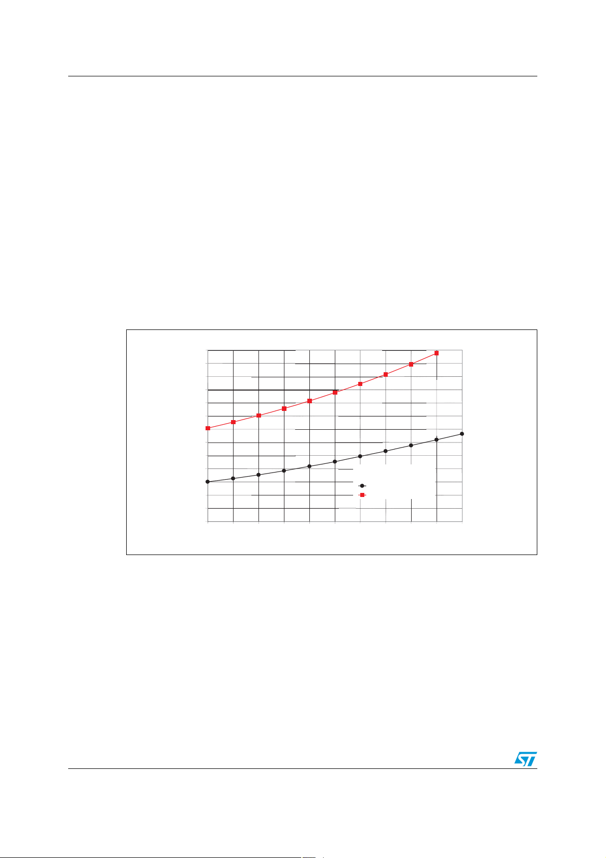
The gate current value (Pin G - to turn on the AC switch) is defined by the external resistor
R
value (resistor connected between the STCC08 RIG input and ground). Figure 4 gives
IG
the maximum value of this resistor (R
temperature (T
amb_min
switch junction temperature increases when the AC switch is on (T
current required to turn on the AC switch decreases (I
ambient temperature has to be considered.
Ö the AC switch is turned on
CC
) according to the minimum ambient
IG_max
) of the appliance for two AC switch IGT values. Note that as the AC
> T
< IGT). So only the minimum
G
j
), the IG gate
amb
Figure 4. Resistor R
AC switch I
R
130
120
110
100
90
80
70
60
50
40
30
20
10
0
-20-15-10-5 0 5 1015202530
value according to the minimum ambient temperature and
IG
GT
IG_max
For example, with a 10 mA I
maximum 30 Ω R
resistor can be used to turn on the AC switch throughout the whole
IG
appliance temperature range.
()Ω
IGTAC Switch:
IGT 10mA @ 25°C
IGT 5mA @ 25 °C
T
amb_min
AC switch and a -20 °C minimum ambient temperature, a
GT
(°C)
1.4 AC switch failure mode detection
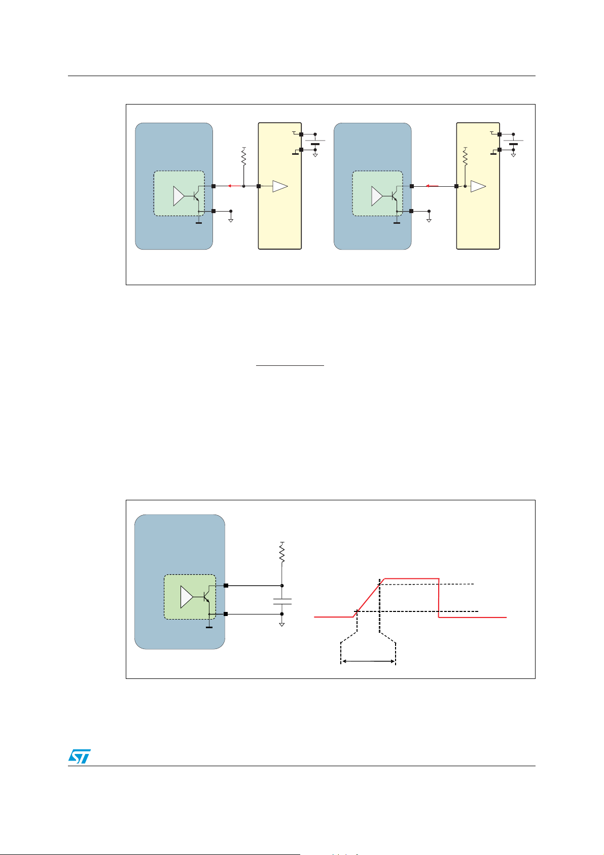
1.4.1 STCC08 AVF output configuration
The STCC08 AVF driver block is used to send the AC switch state to the MCU (see
Section 1.4.2). The STCC08 AVF output is an open collector and can be loaded with an
external resistor (R
Figure 5).
6/28 Doc ID 14460 Rev 2
) or connected directly to the MCU, in pull-up input configuration (see
AVF
Page 7
AN2716 STCC08 description
Figure 5. STCC08 AVF output configuration
PULL-UP
R
V
CC
PULL-UP
= 5.5 V,
STCC08
STCC08
AVF driver
(a) AVF output loaded with an external resistor (R )
The I
defines the minimal R
the R
current in the STCC08 AVF pin must be lower than 5 mA (I
AVF
or R
AVF
PULL-UP
V
CC
R
AVF
AVF
I
AVF
GND
MCU
or pull-up resistor value to use. For example, with V
AVF
resistor value must be higher than 1.1 kΩ to fulfill this condition.
V
CC
STCC08
STCC08
AVF driver
(b) AVF output loaded with the MCU pull-up resistor (R )
AVF
AVF
GND
I
AVF
AVF _max
V
CC
MCU
). Equation 1
CC_max
Equation 1
V
maxCC
or R
_
(
maxAVF
_
PULL-UP
)
mA5
resistor values modify the AVF signal rise time
or
AVF
RorR
_
PULLminAVF
-
>
minUP
_
I
The AVF signal toggles from VCC to GND according to the AC switch state and the AC line
(see Section 1.4.2). The R
(t
R
). This rise time increases with the MCU I/O pin capacitance and R
R_AVF
PULL-UP
resistors. To limit the influence of this delay on the AC switch state detection (see
AVF
Section 1.4.2) and on the ZVS detection application (see Section 4), a 300 kΩ maximum
R
or R
AVF
PULL-UP
300 kΩ maximum R
resistor value is recommended. With a 47 pF CL load capacitor and a
resistor, the AVF rise time is typically about 50 µs (see Figure 6).
AVF
Figure 6. AVF signal rising time measurement information
R
= 300 KΩ
STCC08
STCC08
AVF driver
AVF
AVF
GND
V
CC
R
AVF
C
L
V
AVF
Doc ID 14460 Rev 2 7/28
AVF
CL= 47 pF
t
R_AVF
90 % V
10 % V
CC
CC
Page 8
STCC08 description AN2716
1.4.2 AC switch state detection principle
The AC switch state detection is achieved thanks to the STCC08 “power switch signal
shaping” block. This block measures the current (I
is the image of the AC switch voltage (V
) during both AC line cycle (V
T
Figure 7, three cases can be considered.
● Case 1: If the AC switch is off (V
= V
T
Line
line (see Section 1.5.1), flows through resistor R
case, the STCC08 AVF output signal (V
● Case 2: If the AC switch is on (V
T
this case, the AVF output signal (V
● Case 3: If the AC switch is off and the AC line voltage falls to zero voltage, no I
current flows through the resistor R
AVF
≈ 0), no IAC current flows through the resistor RAC. In
) remains at low level state (GND).
AVF
. In this case, the AVF output signal (V
AC
to zero level (GND).
Knowing the STCC08 IN input state, the MCU is then able to determine the AC switch state
by analyzing the AVF signal (see Section 1.4.3).
Figure 7. AC switch failure detection principle
) through the STCC08 AC input, which
AC
), a low I
AC
current, in phase shift with the AC
AC
for the both AC line polarities. In this
). As illustrated in
Line
) remains at high level state (+VCC).
AVF
AC
) goes
V
T
I
AC
1
3
1
3
1
AVF
The I
V
AC switch off
current follows the waveform of the voltage across the AC switch. The AVF signal
AC
toggles between V
Figure 7). The I
Table 2. I
ACT
electrical parameter dispersion
ACT
I
ACT
The IAC peak current value (I
I
Load
I
ACT
-I
ACT
3
1
and zero level (GND) at a certain IAC current value noted as I
CC
2
AC switch on
t (s)
t (s)
t (s)
Neutral
Line
V
Line
Shunt
R
V
T
Load
I
LOAD
STCC08
STCC08
G
ACS
AC
V
CC
R
I
AC
AC
Power switch
signal shaping
electrical parameter dispersion is shown in Table 2.
AC-peak
Maximum (I
ACT_max
236 µA 82 µA
) must be lower than 2.2 mA (maximum IAC current
) Minimum (I
allowed through STCC08 AC input). Equation 2 defines the minimum resistor R
(R
example, with V
) to limit this IAC current in the worst case (if the AC load fails in short circuit). For
AC_Min
Line_rms_max
= 230 V + 10%, the RAC resistor value must be higher than
163 kΩ.
AVF
ACT
ACT_min
value
AC
V
CC
R
)
AVF
V
AVF
(see
8/28 Doc ID 14460 Rev 2
Page 9
AN2716 STCC08 description
_
Equation 2
V
2
R
AC
>
min
_
X
maxpeakAC
__
maxrmsLine
__
()
mAI
2.2
The resistor R
is used to detect the AC switch state whatever the AC load state is
Shunt
(connected or disconnected). Without this resistor, the STCC08 AVF signal remains at low
level (GND) whatever the AC switch state when the AC load is disconnected (I
detect the AC switch state when the AC load is disconnected (with the resistor R
I
AC-peak
current remains higher than the I
ACT_Max
current (IAC current threshold to ensure
the AC switch state detection - see Ta ble 2). Equation 3 defines the condition on R
R
resistors to ensure a right AC switch states detection in the worst case (if the AC load
Shunt
is disconnected). For example, with V
plus the R
resistor value must be lower than 1.24 MΩ.
Shunt
Line_RMS_Min
= 230 V - 10%, the RAC resistor value
= 0). To
AC
Shunt
AC
), the
and
Equation 3
2 X
RR
_
<+
_
maxACmaxShunt
I
maxACT
To limit the power dissipation by resistors R
V
__
minrmsLine
(236 µA)
AC
and R
lower than ¼ W and their
Shunt
influences on the AC load, a 300 kΩ and 100 kΩ minimum value is recommended
respectively under 230 V rms and 100 V rms AC line. Equation 4 and Equation 5 give the
power dissipation for R
and R
AC
in the worst case.
Shunt
Equation 4
2
(P
)
(V
=
maxRAC
R
)
maxrmsLine
__
minAC
_
Equation 5
2
(P
)
(V
=
maxRShunt
R
)
maxrmsLine
__
minShunt
_
1.4.3 AC switch failures detection during normal operation
Knowing the STCC08 IN input state, the MCU is able to determine the AC switch state by
analyzing the AVF signal. Figure 8 andTable 3 give the AC switch failure modes according to
the AVF signal state and the STCC08 IN signal state. In case of AC switch failure, the MCU
can put the appliance in a safe configuration by switching off an appliance front-end relay.
Doc ID 14460 Rev 2 9/28
Page 10

STCC08 description AN2716
Figure 8. AC switch failure detection
V
V
Line
V
Line
Line
V
Line
VCC/COM
AC switch
Line
Load
RShunt
I
Load
RAC
STCC08
AC
AVF
VCC
R
AVF
V
AVF
VCC
V
AVF
I
Load
(a) AC switch state: off (no failure) if IN = 0 or open circuit failure if IN = 1
VCC
R
VCC/COM
I
AC switch
Line
Load
RShunt
Load
V
Line
RAC
STCC08
AVF
AC
AVF
V
AVF
VCC
I
Load
V
AVF
(b) AC switch state: on (no failure) if IN = 1 or short circuit failure if IN = 0
V
Line
VCC/COM
AC switch
Line
Load
I
Load
RAC
STCC08
AC
AVF
VCC
R
AVF
V
AVF
VCC
I
Load
V
AVF
V
Line
RShunt
(c) AC switch state: positive diode mode failure if IN = 0
VCC/COM
AC switch
Line
Load
RShunt
I
Load
RAC
STCC08
AC
AVF
VCC
V
AVF
R
AVF
VCC
I
Load
V
AVF
(d) AC switch state: negative diode mode failure if IN = 0
V
Line
10/28 Doc ID 14460 Rev 2
Page 11

AN2716 STCC08 description
Table 3. STCC08 status truth table
MCU control (IN) AVF output state
(1)
AC switch state
0+V
0 Toggle from +V
(Except at each zero crossing of the AC line) Off (no failure)
CC
to 0 Diode mode
CC
0 0 Short-circuit
1 0 On (no failure)
1+V
1. The AVF output must be loaded with an external resistor (R
up input configuration (see Section 1.4.1).
(Except at each zero crossing of the AC line) Open-circuit
CC
AVF
1.5 AVF signal reading synchronization
1.5.1 Detection window width definition
When the AC switch is off (not controlled or failed in open circuit), an IAC current flows
through the STCC08 AC input. The value of this current depends on R
resistors, the AC line voltage, and the AC load impedance. The AVF signal toggles between
V
and zero level (GND) for an IAC current value noted I
CC
impact on the AC switch state detection. If the STCC08 is not controlled (IN = 0) and the
AVF signal is read when the I
as failed in short circuit (see Table 3).
Figure 9. STCC08 AVF version when the AC switch is off
current is lower than I
AC
) or connected directly to the MCU, in pull
and R
AC
(see Figure 9). This has an
ACT
, the AC switch can be interpreted
ACT
shunt
Note:
V
Line
I
I
ACT
-I
ACT
AVF
ϕ
AC
A
00=
t
φ
is the phase shift between the AC line and the IAC current when the AC switch is off.
AC
t
1
AC
B
t
2
C
1
1
t
t
2
F
x=2
f
´=2
This phase shift is very low and can be neglected for most AC loads found in home
appliances (see Appendix A).
t (s)
t (s)
Doc ID 14460 Rev 2 11/28
Page 12

STCC08 description AN2716
The t1 and t2 values are defined in Appendix A. For example, with RAC = R
F = 50 Hz, V
AC_Line
respectively equal to 0.1 A and 90°, t
= 230 V, a minimum rms current and a phase shift of the AC load
and t2 are respectively 1.7 ms and 8.3ms.
1
Shunt
= 300 kΩ,
When the AC switch is failed in diode mode, the AC switch is on during only half of the AC
line cycle for resistive load (the load current is in phase with the AC line voltage). In this
case, the AVF signal falls to GND at each cycle of the AC line when the AC switch is on.
However, with an inductive load, the load current (I
) falls to zero after the zero crossing
Load
of the AC line voltage (See Figure 10). This has an impact on the AC switch state detection.
If the AC switch has failed in diode mode and the STCC08 AVF signal is read just after each
zero crossing of the AC line voltage, the AC switch failed in diode mode will not be
discriminated from the AC switch short circuit failure.
Figure 10. Load current and STCC08 AVF variation when the AC switch is failed in
diode mode
V
Line
I
Load
IN
t (s)
t (s)
AVF
t (s)
t
Δ
Detection
t
READAVF
_
The STCC08 AVF signal should be read after the AC line peak voltage (t
Equation 6) and before the time t
to detect all AC switch states for most home
2
t
2
AVF_READ
) (See
appliance loads.
Equation 6
t
AVF_READ
Note: Note, if the STCC08 AVF signal is read between times t1 and t2 (see Figure 9), all the AC
switch failures will be detected but the AC switch failed in diode mode will be confused with
the AC switch failed in short-circuit.
To detect the AC switch state when the STCC08 is controlled by a pulsed gate current, the
MCU should store the IN signal state in a RAM register. This RAM register could be
initialized at each zero crossing of the AC line voltage.
1
>
F
·4
Min
12/28 Doc ID 14460 Rev 2
Page 13

AN2716 STCC08 description
1.5.2 AC switch state detection after IN signal removal
When the IN signal is removed (to turn on or off the AC switch), a parasitic detection of the
AC switch state exists up to the next AC load current zero (see Figure 11 for AC inductive
load case). As the AVF signal remains at a low-level state when the control is removed
(I
≠ 0), the AC switch can be interpreted as an AC switch short circuit failure.
LOAD
Figure 11. Parasitic detection for inductive load
V
Line
I
Load
t (s)
IN
t (s)
I
AC
AVF
t
Delay
Parasitic detection
I
ACT
-I
ACT
t (s)
t (s)
To ensure a correct detection of the AC switch state and to take into account the AC switch
failed in diode mode, when the IN control is removed and whatever the AC load used, the
AVF reading must be carried out according to Equation 7. For example, with F = 50 Hz, the
AVF signal can be read after 20 ms when the IN control has been removed.
Equation 7
t
min
_
Delay
Note: Overall, the AVF signal should be read during several AC line cycles to avoid an incorrect
interpretation of the AC switch state.
1
>
F
Doc ID 14460 Rev 2 13/28
Page 14

STCC08 consumption AN2716
2 STCC08 consumption
Equation 8, Figure 12, and Tabl e 4 define the maximum STCC08 current consumption
(I
DC_max
from the AC line and not from the STCC08 DC power supply. The current I
current to turn on the AC switch, defined according to the external resistor R
Figure 13). The current I
I
Quiescent
100 µA. The AVF current, used to polarize the STCC08 AVF output is defined by the resistor
R
AVF
Equation 8
Figure 12. STCC08 current consumption
). The current IAC is used only to detect the AC switch states. This current comes
is the gate
G
Quiescent
defines the STCC08 quiescent current. The maximum
current is specified at 2 mA. The maximum IN input current (I
IG
) is specified at
IN_Max
or by the MCU pull up resistor (see Equation 9).
IIIII
+++=
maxINmaxQuiesientmaxAVFG_maxmaxDC
____
Neutral
STCC08
AVF
I
Quiescent
R
AVF
I
AVF
I
G
G
VCC
value (see
I
DC
V
DC
MCU
I
R
AC
Line
Table 4. STCC08 consumption values
Load
R
Shunt
AC
AC
GND
IN
I
IN
Parameter Definition Maximum value
I
G_max
I
Quiescent
I
AVF
I
IN
AC switch gate current
STCC08 current consumption 2 mA
AVF pin collector current
IN input current (to control the AC switch) 100 µA
Depends on the R
Figure 13
Depends on the R
(I
AVF _max
= 5 mA). See Equation 9
Equation 9
V
maxCC
=
maxAVFI_
_
R
minAVF
_
=
V
_
R
Pull-up_min
maxCC
resistor. See
IG
resistor
AVF
14/28 Doc ID 14460 Rev 2
Page 15

AN2716 STCC08 consumption
Figure 13. Maximum IG current (I
I
G_max
28
26
24
22
20
18
16
14
12
10
8
6
4
2
0
For example, with R
(mA)
30 35 40 45 50 55 60 65 70 75 80 85 90 95 100 105 110 115 120
= 30 Ω, V
IG
CC_max
current consumption is about 30 mA.
) versus resistor RIG value
G_max
R
(Ω)
IG_min
= 5.5 V and R
= 10 kΩ, the maximum STCC08
AVF
Doc ID 14460 Rev 2 15/28
Page 16

Recommended component values AN2716
3 Recommended component values
Figure 14 and Table 5 show the application diagram and the recommended values to
implement the STCC08 device in the appliance according the AC line voltage.
Figure 14. Application diagram
Neutral
ACS
R
Load
RShunt
Line
Front end relay
Table 5. Recommended value
R
Shunt
R
AC
R
AVF
AC
G
V
CC
C
AC
IGT = 10 mA @ -20 °C 30 Ω ± 1% @ ¼ W 30 Ω ± 1% @ ¼ W
R
IG
I
= 5 mA @ -20 °C 68 Ω ± 1% @ ¼ W 68 Ω ± 1% @ ¼ W
GT
C 33 nF 33 nF
t
AVF_READ
t
(see Appendix A) 8.3 ms 8.9 ms
2_min
Δt
Detection_min
VCC= 3.3V to 5V
IN
R
IG
R
AVF
AVF
GND
GND
IG
V
CC
R
AVF
MCU
STCC08
V
Line
230 V rms at 50 Hz 110 V rms at 50 Hz
300 kΩ @ ¼ W 100 kΩ @ ¼ W
300 kΩ @ ¼ W 100 kΩ @ ¼ W
10 kΩ @ ¼ W 10 kΩ @ ¼ W
5.1 ms 5.1 ms
3.2 ms 3.8 ms
V
GND
CC
16/28 Doc ID 14460 Rev 2
Page 17

AN2716 ZVS detection application
4 ZVS detection application
The STCC08 “Power switch signal shaping” block can be used to detect the zero crossing of
the AC line voltage. The resistor R
as shown in Figure 15. The AVF signal toggles between V
crossing of the AC line voltage.
Figure 15. ZVS detection
Neutral
ACS
V
AC
V
CC
AC
Line
Load
RShunt
R
AC
must be connected between AC input and the AC line
AC
G
Power switch
signal shaping
Gate driver
+
-
STCC08
STCC08
and zero level at each zero
CC
3.3 V to 5 V
IN
R
IG
V
AVF driver
AVF
GND
CC
MCU
V
CC
V
AC
AVF
Δ
t
t
AVF
AVF
Equation 10 defines the maximal AVF signal low level width (Δt
the AC line voltage according to the value of resistor R
AC
.
Equation 10
⎛
⎜
t
Δ
maxAVF
_
··1π
Ar
sin
X=
F
min
⎜
⎝
RI
·
V
·2
rms
⎞
maxACmaxACT
__
⎟
⎟
min
_
⎠
t (s)
t (s)
) at each zero crossing of
AVF
Doc ID 14460 Rev 2 17/28
Page 18

Electromagnetic compatibility (EMC) tests AN2716
5 Electromagnetic compatibility (EMC) tests
5.1 Demonstration board description
The STCC08 has been tested using a stand-alone demonstration board (see Appendix B)
and according to IEC 61000-4-4. Appendix C and Appendix D give respectively the
electrical schematic and the layout of the demonstration board. This demonstration board
can work on 110 V / 230 V rms 50 / 60 Hz mains voltage. The STCC08 board includes:
● The STCC08
● The ACS108-6S
● An STLITE39 MCU.
● A capacitive power supply (C15 = 10 nF)
● An In-dart connector to load the MCU firmware
● Mechanical switches used to simulate different AC switch failures (diode mode, short
circuit and open circuit)
● A mechanical switch to control the STCC08 IN signal through MCU
● LEDs used to visualize the detected ACS failure modes.
● An AC load: light bulb (15 W at 230 V rms)
The STLITE39 MCU is used to turn the ACS108-6S on / off through the STCC08 and to
analyze the AVF signal to power LEDs indicating AC switch states and failures (AC switch
ON, diode mode, short circuit and open circuit).
Regarding the power supply, the maximum average current absorbed by the board is about
48 mA. A 2.2 µF C16 capacitor has been used to ensure the board works correctly (see
Appendix C).
5.2 IEC 61000-4-4 burst immunity test
5.2.1 Test conditions
● Ambient temperature: 25°C
● Relative humidity: 35%
5.2.2 Demonstration board immunity test
The AC line input X2 capacitor C15 (10 nF) is used to help avoid triggering the AC switch
(ACS108-6S). The MCU program reads the AVF signal at each AC line peak voltage (see
Figure 16). The demonstration board is validated if the AVF signal remains at the same level
during three consecutive AC line cycles.
18/28 Doc ID 14460 Rev 2
Page 19

AN2716 Electromagnetic compatibility (EMC) tests
Figure 16. AVF signal detection
Timer
> T/4 ms
T/2 ms
ZVS delay
Read AVF and timer off
ZVS detection => Timer on
ZVS delay
ZVS detection => Timer on
The demonstration board and mains wires are placed 10 cm above the ground reference.
The mains wire is shorter than 1 m. Each operating cycle has been tested (load off and on).
The demonstration board supports burst levels higher than 4 kV without spurious triggering
of the ACS or ST7Lite3 MCU loss whatever the coupling mode (to L, N, etc.).
5.2.3 Advice to improve the application immunity
V
AC
Read AVF and timer of
To improve the application performance in term of EMC, the software must be EMC oriented
(for more information please refer to the application note AN1015):
● Auto-recovery routine. At each reset interrupt, the program must check if the data
stored in the RAM are as scheduled or not. A reset can occur without the supply
voltage having fallen below V
(data retention parameter). In this case, a full start-up
RM
is not necessary, and the program can keep working with the previous RAM data. This
is helpful to avoid missing load control and the AC switch status when a reset occurs
due to an EMI problem, for example. If the checked RAM registers are not as expected,
then a complete initialization procedure is launched. If the RAM area is adequate, then
a “smart reset” can be performed. Only the registers that are used to store internal subroutine variables are cleared. Only the main registers keep their previous values (AC
switch status, AC switch control …).
● Using the watchdog properly. Enable the watchdog as soon as possible after reset
and never refresh the watchdog in an interrupt routine.
● Secure the unused program memory area. Fill the unused memory locations with
code that forces a watchdog reset or jumps to a known program
location if you do not
want to generate a reset.
● Input filtering. It is recommended that the AVF signal be read during several AC line
cycles.
Doc ID 14460 Rev 2 19/28
Page 20

Conclusion AN2716
6 Conclusion
This application note illustrates how designers can maximize the STCC08 performance in
their appliances especially for AC switch state detection and EMI robustness.
This document describes the STCC08 device and gives technical recommendations about
the STCC08 implementation in the appliance.
References
1. T. Castagnet, B. Cheron, A. Edet, “AC power management in homes appliances: a
reality to save energy and increase safety”, IATC 2006, Rosemont, Illinois, USA.
2. L.Gonthier, "A New Solid State Switch for Home Appliances", International Appliance
Technical Conference, IATC 1999, West Lafayette, Indiana, USA.
3. G. Benabdelaziz, P. Paillet, “AC STCC08 - Safety supervisor for home-appliance AC
switches”, PCIM 2009, Nuremberg, Germany.
20/28 Doc ID 14460 Rev 2
Page 21

AN2716 Timing definitions
Appendix A Timing definitions
When the AC switch is OFF (not controlled or failed in open circuit), an IAC current flows
through the STCC08 AC input. The value of this current depends on RAC and Rshunt
resistors, the AC line voltage and the AC load impedance. The AVF signal toggles between
VCC and zero level (GND) for an IAC current value noted IACT (see Figure 17).
Figure 17. Detection window width of the AC switch state
V
Line
I
AC
t (s)
-I
I
ACT
ACT
AVF
ϕ
AC
A
00=
t
Considering Figure 18, the I
t
1
current variation, when the AC switch is off, is defined
AC
according to Equation 11 where I
B
AC_peak
R and L are AC load characteristics, and φ
AC line voltage.
t (s)
C
1
1
t
t
2
t
2
F
x=2
f
´=2
is the peak IAC current, F is the AC line frequency,
is the phase shift between IAC current and the
AC
Doc ID 14460 Rev 2 21/28
Page 22

Timing definitions AN2716
Figure 18. AC load model definition
Neutral
Line
V
AC switch
V
CC
STCC08
STCC08
Load
LR
R
AC
I
AC
AC
Power switch
signal shaping
R
Shunt
Equation 11
() ( )
_
Considering Equation 11, t1 and t2 times are given respectively by Equation 12 and
Equation 13 in the worst case (to avoid the false detection of an AC switch failed in short-
circuit any time).
tFItI ϕπ -=···2sin·
ACpeakACAC
Equation 12
⎛
=
t ϕ
_1
Max
1
xx
2
π
⎡
Ar
⎢
F
⎢
min
⎣
I
⎜
sin·
⎜
I
⎝
⎞
_
maxAC T
⎟
+
⎟
__
minPeakAC
⎠
AC
⎤
⎥
max_
⎥
⎦
Equation 13
⎛
F
max
⎡
⎜
⎢
-
⎜
⎢
⎝
⎣
t
=
_2
min
1
xx
2
π
Ar
⎛
I
⎜
sin·
⎜
I
⎝
⎞
_
maxACT
⎟
+
ϕπ
⎟
__
minPeakAC
⎠
⎞
⎤
⎟
⎥
_
maxAC
⎟
⎥
⎠
⎦
I
AC_peak_min
defines the minimum peak IAC current through the STCC08 AC input to ensure
the AC switch state detection. This current must be higher than the maximum specified I
parameter (I
ACT_max
) in order to detect the AC switch state in the worst case (when the AC
load is disconnected). Equation 14 defines this condition. Indeed, when the AC load is
disconnected, the I
= R
10%, the I
= 300 kΩ (see Equation 2 and Equation 3), F = 50 Hz and V
Shunt
AC_Peak_min
current is limited by RAC and R
AC
is 465 µA.
Equation 14
·2
I
=>
minPeakAC
__
V
φAC is the phase shift between the AC line and the IAC current when the AC switch is off. As
the resistor R
value is higher than the most AC load impedances found in home
Shunt
appliances, this phase shift depends only on the AC load characteristic and resistor R
Figure 19 gives Fresnel's diagram for R
22/28 Doc ID 14460 Rev 2
minrmsLine
__
+
RR
maxACmaxShunt
__
I
ACT_max (236 µA)
= 0 and RAC ≠ 0 for the circuit in Figure 18 to
AC
resistors. For example, with RAC
Shunt
Line_RMS_min
ACT
= 230 V -
.
AC
Page 23

AN2716 Timing definitions
define the φAC phase shift. If RAC = 0 Ω, the rms IAC current and φAC phase shift are equal
respectively to rms I
R
≠ 0 Ω, the rms IAC current (I
AC
resistor R
the maximum φ
and the AC load impedance. In this case, and according to Fresnel's diagram,
AC
AC
Load
current (I
Load_RMS
AC_RMS
) and φ
phase shift of the AC load. If
Load
) and φAC phase shift depend on the value of the
phase shift is defined by Equation 15 and Equation 16.
Equation 15
x
π
2
V
rmsLine
_
x
=
xx
rmsAC
() ()
ϕ
sin
AC
=
π
2
sin
IFLIFL
xxxx
ϕ
Load
rmsLoad
__
Equation 16
⎞
⎟
⎟
⎠
AC_max
Arc ϕϕ sinsin
⎛
I
rms_maxAC
_
⎜
⎜
I
rms_minLoad
_
⎝
()
x=
Load_max
For example, in the worst case, if the minimum rms current (I
φ
phase shift of the AC load are respectively 0.1 A and 90°, the maximum φAC phase
Load
shift is about 1.26 °. This phase shift is very low and can be neglected as most AC loads
have rms current higher than 0.1 A and phase shift lower than 90°. With R
= 300 kΩ and F = 50 Hz, t
1_max
and t
are respectively 1.7 ms and 8.3 ms.
2_min
Figure 19. Fresnel’s diagram
V
Line_RMS
φ
AC
φ
Load
R . I
Load_RMS
(RAC= 0)
(R + RAC).I
AC_RMS
2 . p .f . L .I
Note: If the AC load is a resistor, or is disconnected, the I
(φ
= 0).
AC
The STCC08 AVF signal should be read after the AC line peak voltage and before the t
time to detect all AC switch states for most home appliance loads.
Load_min
2 . π .f .L .I
Load_RMS
current is in phase with the AC line
AC
) and the maximum
= R
AC
Shunt
AC_RMS
2
Doc ID 14460 Rev 2 23/28
Page 24

Demonstration board component layout AN2716
Appendix B Demonstration board component layout
Figure 20. Demonstration board component layout
24/28 Doc ID 14460 Rev 2
Page 25

AN2716 Demonstration board schematic
Appendix C Demonstration board schematic
Figure 21. Demonstration board schematic
COM/VCC
ON/OFF
ON/OFF
COM/VCC
D9
D9
ON
ON
D8
D8
CC
CC
OPEN
OPEN
D7
D7
D6
D6
DIODE
DIODE
D5
D5
STCC08 CNTRL
STCC08 CNTRL
C10
C10
10n
10n
ZVS
ZVS
C11
C11
10n
10n
C12
C12
10n
10n
C13
C13
10n
10n
ST CC0 8 CNTRL
SW5
SW5
COM/VCC
COM/VCC
ST CC0 8 CNTRL
AC
AC
OUT
OUT
TP6
TP6
Gate
Gate
ACS
ACS
U3
U3
D4
D4
1N4007
1N4007
SW3
SW3
D3
D3
SW2
SW2
1N4007
1N4007
SW4
SW4
2
2
1
1
J2
J2
J2 -Light Bulb- 15W
J2 -Light Bulb- 15W
TP7
TP7
AC
AC
56k
56k
R4
R4
56k
56k
R3
R3
56k
56k
R2
R2
56k
56k
R1
R1
56k
56k
56k
56k
56k
56k
56k
R5
R6
R5
R6
56k
R7
R8
R7
R8
J3
COM/VCC
COM/VCC
RST
RST
TP9
TP9
IN
IN
IN_MCU
IN_MCU
Com/VCC
Com/VCC
TP3
TP3
COM/VCC
COM/VCC
2
2
F1
F1
FUSE/1A
FUSE/1A
TP1
TP1
N
N
GND
GND
ZVS
ZVS
TP5
TP4
TP5
TP4
ZVS
ZVS
100n/16V
100n/16V
C2
C2
+
+
C1
C1
2200uF/25V
2200uF/25V
D1
D1
5V6 - 0.5W
5V6 - 0.5W
1
1
Varistor 375V
Varistor 375V
R13
R13
C15
C15
J1
J1
R12
R12
1N4148
1N4148
D2
D2
R11
R11
C16
C16
2.2uF - X2
2.2uF - X2
R10
R10
R14
R14
39 - 3W
39 - 3W
R9
R9
10n - X2
10n - X2
123
123
AC Mains
AC Mains
COM/VCC
COM/VCC
C16
C16
1n
1n
68k
68k
TP8
TP8
AVF
AVF
AC
AC
68k
68k
C14
C14
100n
100n
4
4
68k
68k
AC
AC
U1
U1
5
5
68k
68k
100n/16V
100n/16V
C3
C3
COM/VCC
COM/VCC
TP2
TP2
L
L
C9
C9
C8
C8
R24
R24
3
3
120n/16V
120n/16V
120n/16V
120n/16V
NC
NC
GATE6VCC
GATE6VCC
43
43
Gate
Gate
INDART CONNECTOR :HE10
INDART CONNECTOR :HE10
R22
R22
470
470
R21
R21
470
470
R20
R20
470
470
R19
R19
470
470
LS
LS
R18
R18
470
470
19
19
20
20
OSC2
OSC2
OSCI/CLKIN
OSCI/CLKIN
U2
U2
VDD
VDD
VSS
VSS
2
2
1
1
COM/VCC
COM/VCC
1.2K
1.2K
2
2
1
1
IN
IN
AVF
AVF
GND
GND
RIG
RIG
8
8
7
7
R23
R23
PA0(HS)18PA1(HS)17PA2(HS)16PA3(HS)15PA5(HS)
PA0(HS)18PA1(HS)17PA2(HS)16PA3(HS)15PA5(HS)
RST
RST
3
3
RST
RST
IN_MCU
IN_MCU
STCC08
STCC08
4
4
R17
R17
PB0/AIN0
PB0/AIN0
5
5
PB1/AIN1
PB2/AIN2
PB1/AIN1
PB2/AIN2
6
6
IN_MCU
IN_MCU
R16
11
11
13
12
13
12
14
14
PA4(HS)
PA6(HS)
PA4(HS)
PA6(HS)
PA7/TDO
PA7/TDO
ST7LITE39
ST7LITE39
PB6/RDI10PB5/AIN59PB4/AIN48PB3/AIN3
PB6/RDI10PB5/AIN59PB4/AIN48PB3/AIN3
7
7
TP12
TP12
C7
C7
100n/16V
100n/16V
0
0
C6
C6
10n/16V
10n/16V
C5
C5
10n/16V
10n/16V
0k
C4
C4
10n/16V
10n/16V
R15
R15
680k
680k
SW1
SW1
123456789
10
123456789
10
J3
Doc ID 14460 Rev 2 25/28
Page 26

Demonstration board circuit layout view AN2716
Appendix D Demonstration board circuit layout view
Figure 22. Top layer view
Figure 23. Bottom layer view
26/28 Doc ID 14460 Rev 2
Page 27

AN2716 Revision history
Revision history
Table 6. Document revision history
Date Revision Changes
26-Nov-2008 1 Initial release.
16-Jun-2010 2 Revised Section 1.5.1 and Appendix A. Added References.
Doc ID 14460 Rev 2 27/28
Page 28

AN2716
Please Read Carefully:
Information in this document is provided solely in connection with ST products. STMicroelectronics NV and its subsidiaries (“ST”) reserve the
right to make changes, corrections, modifications or improvements, to this document, and the products and services described herein at any
time, without notice.
All ST products are sold pursuant to ST’s terms and conditions of sale.
Purchasers are solely responsible for the choice, selection and use of the ST products and services described herein, and ST assumes no
liability whatsoever relating to the choice, selection or use of the ST products and services described herein.
No license, express or implied, by estoppel or otherwise, to any intellectual property rights is granted under this document. If any part of this
document refers to any third party products or services it shall not be deemed a license grant by ST for the use of such third party products
or services, or any intellectual property contained therein or considered as a warranty covering the use in any manner whatsoever of such
third party products or services or any intellectual property contained therein.
UNLESS OTHERWISE SET FORTH IN ST’S TERMS AND CONDITIONS OF SALE ST DISCLAIMS ANY EXPRESS OR IMPLIED
WARRANTY WITH RESPECT TO THE USE AND/OR SALE OF ST PRODUCTS INCLUDING WITHOUT LIMITATION IMPLIED
WARRANTIES OF MERCHANTABILITY, FITNESS FOR A PARTICULAR PURPOSE (AND THEIR EQUIVALENTS UNDER THE LAWS
OF ANY JURISDICTION), OR INFRINGEMENT OF ANY PATENT, COPYRIGHT OR OTHER INTELLECTUAL PROPERTY RIGHT.
UNLESS EXPRESSLY APPROVED IN WRITING BY AN AUTHORIZED ST REPRESENTATIVE, ST PRODUCTS ARE NOT
RECOMMENDED, AUTHORIZED OR WARRANTED FOR USE IN MILITARY, AIR CRAFT, SPACE, LIFE SAVING, OR LIFE SUSTAINING
APPLICATIONS, NOR IN PRODUCTS OR SYSTEMS WHERE FAILURE OR MALFUNCTION MAY RESULT IN PERSONAL INJURY,
DEATH, OR SEVERE PROPERTY OR ENVIRONMENTAL DAMAGE. ST PRODUCTS WHICH ARE NOT SPECIFIED AS "AUTOMOTIVE
GRADE" MAY ONLY BE USED IN AUTOMOTIVE APPLICATIONS AT USER’S OWN RISK.
Resale of ST products with provisions different from the statements and/or technical features set forth in this document shall immediately void
any warranty granted by ST for the ST product or service described herein and shall not create or extend in any manner whatsoever, any
liability of ST.
ST and the ST logo are trademarks or registered trademarks of ST in various countries.
Information in this document supersedes and replaces all information previously supplied.
The ST logo is a registered trademark of STMicroelectronics. All other names are the property of their respective owners.
© 2010 STMicroelectronics - All rights reserved
STMicroelectronics group of companies
Australia - Belgium - Brazil - Canada - China - Czech Republic - Finland - France - Germany - Hong Kong - India - Israel - Italy - Japan -
Malaysia - Malta - Morocco - Philippines - Singapore - Spain - Sweden - Switzerland - United Kingdom - United States of America
www.st.com
28/28 Doc ID 14460 Rev 2
 Loading...