

AN2713
Application note
LNB power supply based on the LNBH23 supply
and control IC with step-up and I²C interface
Introduction
This application note is intended to provide additional information and suggestions for the
correct use of the LNBH23 device. All waveforms shown are based on the demonstration
board (order code STEVAL-CBL003V1) described in Section 5.
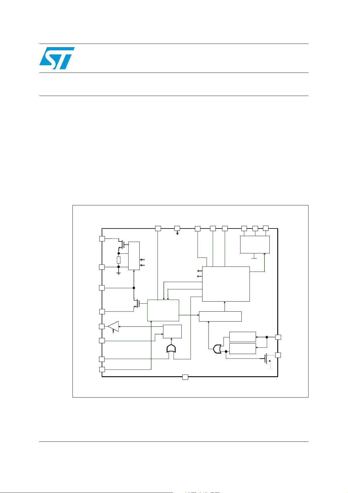
The LNBH23 is an integrated solution for supplying/interfacing satellite LNB modules. It
provides good performance in a simply and cheaply way, with minimum external
components necessary. It includes all functions needed for LNB supply and interfacing, in
accordance with international standards. Moreover, it includes an I
thanks to a fully integrated step-up DC-DC converter, it functions with a single input voltage
supply ranging from 8 V to 15 V.
Figure 1. LNBH23 internal block diagram
2
C bus interface and,
SDA SCL
ADDR
LX
PWM
Controller
Rsense
P-GND
Vup
VoRX
VoTX
EXTM
DSQIN
VCTRL
TTX
EN
VSEL
Linear Post-reg
+Modulator
+Protections
+Diagnostics
VOUT Control
22KHz
Oscill.
LNBH23
A-GND
VSEL
TTX
ITEST
TEN
I²C interface
I²C Diagnostics
22KHz Tone
Amp. Diagn.
22KHz Tone
Freq. Detector
BypVcc Vcc-LISEL TTX
Preregulator
+U.V.lockout
+P.ON reset
EN
DETIN
DSQOUT
November 2009 Doc ID 14431 Rev 1 1/40
www.st.com

Content AN2713
Content
1 Block diagram description . . . . . . . . . . . . . . . . . . . . . . . . . . . . . . . . . . . . 6
1.1 Step-up controller . . . . . . . . . . . . . . . . . . . . . . . . . . . . . . . . . . . . . . . . . . . . 6
1.2 Pre-regulator block . . . . . . . . . . . . . . . . . . . . . . . . . . . . . . . . . . . . . . . . . . . 6
1.3 I
C interface and diagnostics . . . . . . . . . . . . . . . . . . . . . . . . . . . . . . . . . . . 6
2
1.4 22 kHz oscillator and EXTM function . . . . . . . . . . . . . . . . . . . . . . . . . . . . . 7
1.5 Tone detector . . . . . . . . . . . . . . . . . . . . . . . . . . . . . . . . . . . . . . . . . . . . . . . 7
1.6 DiSEqC communication . . . . . . . . . . . . . . . . . . . . . . . . . . . . . . . . . . . . . . . 8
1.7 Linear post-regulator, modulator and protection . . . . . . . . . . . . . . . . . . . . 8
2 Pin description . . . . . . . . . . . . . . . . . . . . . . . . . . . . . . . . . . . . . . . . . . . . . 9
3 Component selection guidelines . . . . . . . . . . . . . . . . . . . . . . . . . . . . . . 11
3.1 Input capacitors . . . . . . . . . . . . . . . . . . . . . . . . . . . . . . . . . . . . . . . . . . . . 12
3.2 Ferrite bead . . . . . . . . . . . . . . . . . . . . . . . . . . . . . . . . . . . . . . . . . . . . . . . 12
3.3 DC-DC converter output capacitors . . . . . . . . . . . . . . . . . . . . . . . . . . . . . 12
3.4 DC-DC converter Schottky diode . . . . . . . . . . . . . . . . . . . . . . . . . . . . . . . 13
3.5 DC-DC converter inductor . . . . . . . . . . . . . . . . . . . . . . . . . . . . . . . . . . . . 13
3.6 Output current limit-RSEL selection . . . . . . . . . . . . . . . . . . . . . . . . . . . . . 15
3.7 Undervoltage diode protection . . . . . . . . . . . . . . . . . . . . . . . . . . . . . . . . . 15
3.8 DiSEqC implementation and inductor selection . . . . . . . . . . . . . . . . . . . . 15
3.9 TVS diode . . . . . . . . . . . . . . . . . . . . . . . . . . . . . . . . . . . . . . . . . . . . . . . . 16
4 Other application circuits . . . . . . . . . . . . . . . . . . . . . . . . . . . . . . . . . . . . 17
4.1 18 V to 13 V fast transition with high bus capacitance . . . . . . . . . . . . . . . 17
4.2 Reverse voltage and lightning surge protection . . . . . . . . . . . . . . . . . . . . 19
5 Layout guidelines . . . . . . . . . . . . . . . . . . . . . . . . . . . . . . . . . . . . . . . . . . 21
5.1 PCB layout . . . . . . . . . . . . . . . . . . . . . . . . . . . . . . . . . . . . . . . . . . . . . . . . 22
5.2 Startup procedure . . . . . . . . . . . . . . . . . . . . . . . . . . . . . . . . . . . . . . . . . . 24
2/40 Doc ID 14431 Rev 1

AN2713 Content
6 Software installation . . . . . . . . . . . . . . . . . . . . . . . . . . . . . . . . . . . . . . . . 27
6.1 How to use the LNBH23 demonstration board with the LNBxxx control suite
software . . . . . . . . . . . . . . . . . . . . . . . . . . . . . . . . . . . . . . . . . . . . . . . . . . 32
7 Revision history . . . . . . . . . . . . . . . . . . . . . . . . . . . . . . . . . . . . . . . . . . . 39
Doc ID 14431 Rev 1 3/40

List of tables AN2713
List of tables
Table 1. LNBH23 pin description . . . . . . . . . . . . . . . . . . . . . . . . . . . . . . . . . . . . . . . . . . . . . . . . . . . . 9
Table 2. LNBH23 demonstration board BOM list . . . . . . . . . . . . . . . . . . . . . . . . . . . . . . . . . . . . . . . 11
Table 3. Recommended Schottky diode. . . . . . . . . . . . . . . . . . . . . . . . . . . . . . . . . . . . . . . . . . . . . . 13
Table 4. Recommended inductors . . . . . . . . . . . . . . . . . . . . . . . . . . . . . . . . . . . . . . . . . . . . . . . . . . 14
Table 5. Recommended inductors for output R-L filter . . . . . . . . . . . . . . . . . . . . . . . . . . . . . . . . . . . 16
Table 6. Recommended LNBTVS . . . . . . . . . . . . . . . . . . . . . . . . . . . . . . . . . . . . . . . . . . . . . . . . . . 16
Table 7. Document revision history . . . . . . . . . . . . . . . . . . . . . . . . . . . . . . . . . . . . . . . . . . . . . . . . . 39
4/40 Doc ID 14431 Rev 1

AN2713 List of figures
List of figures
Figure 1. LNBH23 internal block diagram . . . . . . . . . . . . . . . . . . . . . . . . . . . . . . . . . . . . . . . . . . . . . . 1
Figure 2. EXTM timing control . . . . . . . . . . . . . . . . . . . . . . . . . . . . . . . . . . . . . . . . . . . . . . . . . . . . . . . 7
Figure 3. DiSEqC timing control. . . . . . . . . . . . . . . . . . . . . . . . . . . . . . . . . . . . . . . . . . . . . . . . . . . . . . 8
Figure 4. LNBH23 pin configuration . . . . . . . . . . . . . . . . . . . . . . . . . . . . . . . . . . . . . . . . . . . . . . . . . . . 9
Figure 5. LNB power supply schematic using the LNBH23 . . . . . . . . . . . . . . . . . . . . . . . . . . . . . . . . 11
Figure 6. External circuit to reduce 18 V to 13 V fall time transition . . . . . . . . . . . . . . . . . . . . . . . . . 17
Figure 7. Fast transition timing sequence . . . . . . . . . . . . . . . . . . . . . . . . . . . . . . . . . . . . . . . . . . . . . 18
Figure 8. Fast transition timing control with 22 kHz tone . . . . . . . . . . . . . . . . . . . . . . . . . . . . . . . . . . 19
Figure 9. External circuit protection schematic . . . . . . . . . . . . . . . . . . . . . . . . . . . . . . . . . . . . . . . . . 20
Figure 10. STEVAL-CBL003V1 demonstration board photo (PowerSSO-24 package). . . . . . . . . . . . 21
Figure 11. STEVAL-CBL005V1 demonstration board photo (QFN32 package) . . . . . . . . . . . . . . . . . 21
Figure 12. STEVAL-CBL003V1 PCB top layer . . . . . . . . . . . . . . . . . . . . . . . . . . . . . . . . . . . . . . . . . . 22
Figure 13. STEVAL-CBL003V1 PCB bottom layer . . . . . . . . . . . . . . . . . . . . . . . . . . . . . . . . . . . . . . . 22
Figure 14. STEVAL-CBL003V1 component layout . . . . . . . . . . . . . . . . . . . . . . . . . . . . . . . . . . . . . . . 23
Figure 15. STEVAL-CBL005V1 PCB top layer . . . . . . . . . . . . . . . . . . . . . . . . . . . . . . . . . . . . . . . . . . 23
Figure 16. STEVAL-CBL005V1 PCB bottom layer . . . . . . . . . . . . . . . . . . . . . . . . . . . . . . . . . . . . . . . 24
Figure 17. STEVAL-CBL005V1 component layout . . . . . . . . . . . . . . . . . . . . . . . . . . . . . . . . . . . . . . . 24
Figure 18. STEVAL-CBL003V1 connectors. . . . . . . . . . . . . . . . . . . . . . . . . . . . . . . . . . . . . . . . . . . . . 25
Figure 19. STEVAL-CBL005V1 connectors. . . . . . . . . . . . . . . . . . . . . . . . . . . . . . . . . . . . . . . . . . . . . 25
Figure 20. STEVAL-CBL003V1 bench test . . . . . . . . . . . . . . . . . . . . . . . . . . . . . . . . . . . . . . . . . . . . . 26
Figure 21. STEVAL-CBL005V1 bench test . . . . . . . . . . . . . . . . . . . . . . . . . . . . . . . . . . . . . . . . . . . . . 26
Figure 22. PC to I
Figure 23. I
Figure 24. Main settings window . . . . . . . . . . . . . . . . . . . . . . . . . . . . . . . . . . . . . . . . . . . . . . . . . . . . . 28
Figure 25. Device selection window. . . . . . . . . . . . . . . . . . . . . . . . . . . . . . . . . . . . . . . . . . . . . . . . . . . 29
Figure 26. Parallel port setting . . . . . . . . . . . . . . . . . . . . . . . . . . . . . . . . . . . . . . . . . . . . . . . . . . . . . . . 29
Figure 27. LPT1 setting . . . . . . . . . . . . . . . . . . . . . . . . . . . . . . . . . . . . . . . . . . . . . . . . . . . . . . . . . . . . 30
Figure 28. Password setting . . . . . . . . . . . . . . . . . . . . . . . . . . . . . . . . . . . . . . . . . . . . . . . . . . . . . . . . 30
Figure 29. I
Figure 30. Autoread setting . . . . . . . . . . . . . . . . . . . . . . . . . . . . . . . . . . . . . . . . . . . . . . . . . . . . . . . . . 31
Figure 31. Power-on at 13.4 V . . . . . . . . . . . . . . . . . . . . . . . . . . . . . . . . . . . . . . . . . . . . . . . . . . . . . . . 32
Figure 32. Power-on at 18.5 V . . . . . . . . . . . . . . . . . . . . . . . . . . . . . . . . . . . . . . . . . . . . . . . . . . . . . . . 33
Figure 33. LLC activation . . . . . . . . . . . . . . . . . . . . . . . . . . . . . . . . . . . . . . . . . . . . . . . . . . . . . . . . . . . 34
Figure 34. Tone activation . . . . . . . . . . . . . . . . . . . . . . . . . . . . . . . . . . . . . . . . . . . . . . . . . . . . . . . . . . 35
Figure 35. Overload detection . . . . . . . . . . . . . . . . . . . . . . . . . . . . . . . . . . . . . . . . . . . . . . . . . . . . . . . 36
Figure 36. Overtemperature detection. . . . . . . . . . . . . . . . . . . . . . . . . . . . . . . . . . . . . . . . . . . . . . . . . 36
Figure 37. PCL deactivation. . . . . . . . . . . . . . . . . . . . . . . . . . . . . . . . . . . . . . . . . . . . . . . . . . . . . . . . . 37
Figure 38. AUX activation . . . . . . . . . . . . . . . . . . . . . . . . . . . . . . . . . . . . . . . . . . . . . . . . . . . . . . . . . . 38
2
2
2
C main window . . . . . . . . . . . . . . . . . . . . . . . . . . . . . . . . . . . . . . . . . . . . . . . . . . . . 27
C bus communication error . . . . . . . . . . . . . . . . . . . . . . . . . . . . . . . . . . . . . . . . . . . . . . . 28
C device address setting . . . . . . . . . . . . . . . . . . . . . . . . . . . . . . . . . . . . . . . . . . . . . . . . . 31
Doc ID 14431 Rev 1 5/40

Block diagram description AN2713
1 Block diagram description
The internal blocks of the LNBH23 are described in the paragraphs that follow.
1.1 Step-up controller
The LNBH23 features a built-in step-up DC-DC converter that, from a single supply source
ranging from 8 V to 15 V, generates the voltages that allow the linear post-regulator to work
with minimum power dissipation. The external components of the DC-DC converter are
connected to the Lx and VUP pins (see Figure 5). No external power MOSFET is needed.
1.2 Pre-regulator block
This block includes a voltage reference connected to the BYP pin, an undervoltage lockout
circuit, intended to disable the whole circuit when the supplied Vcc drops below a fixed
threshold (6.7 V typ) and a power-on reset that sets all the I
Vcc is turned on and rises from zero above the on threshold (7.3 V typ).
2
C registers to zero when the
1.3 I2C interface and diagnostics
The main functions of the device are controlled via I2C bus by writing 5 bits on the system
register (SR bits in write mode). In the same register there are 5 bits that can be read back
(SR bits in read mode) and provide 5 diagnostic functions.
Five bits report the diagnostic status of five internal monitoring functions:
● VMON: output voltage diagnostic. If the output voltage level is below the guaranteed
limit (refer to the device datasheet) the VMON I
● TMON: 22 kHz tone diagnostic. If the 22 kHz tone amplitude and/or the tone frequency
is outside of the guaranteed limits (refer to the device datasheet.), the TMON I
set to "1".
● IMON: minimum output current diagnostic to detect if no LNB is connected on the bus
or a cable not connected to the IRD. The LNBH23 is provided with a minimum output
current flag by the IMON I
lower than 12 mA (typ) with ITEST=1 and 6 mA with ITEST=0.
● OTF: overtemperature flag. If overheating occurs (junction temperature exceeds 150
°C), the OTF I
● OLF: overload flag. If the output current required exceeds the current limit threshold or
2
C bit is set to "1".
a short-circuit occurs, the OLF I
Moreover, three bits will report the last output voltage register status (EN, VSEL, LLC)
received by the IC. The LNBH23 I
addresses by setting the voltage level of the dedicated ADDR pin.
2
C bit in read mode, which is set to "1" if the output current is
2
C bit is set to "1".
2
C interface address can be selected among two different
2
C bit is set to "1".
2
C bit is
6/40 Doc ID 14431 Rev 1
AN2713 Block diagram description
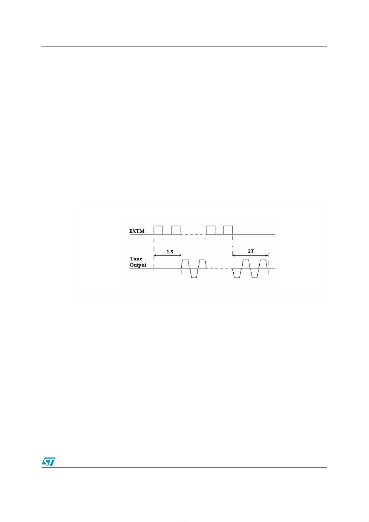
1.4 22 kHz oscillator and EXTM function
The internal 22 kHz tone generator is factory-trimmed in accordance with current standards
and can be controlled by the DSQIN pin (TTL-compatible), which allows immediate
DiSEqC™ data encoding. The rising and falling edges are kept within the 5 µs to 15 µs
range, 8 µs (typ) for 22 kHz. The duty cycle is 50% (typ), and modulates the DC output with
a 0.650 Vpp (typ) amplitude as well as the DSQIN pin.
The EXTM is a logic input to allow the activation of the 22 kHz tone output, on the V
oTx
pin,
by using the device’s integrated tone generator. If the EXTM pin is used, the internal 22 kHz
generator must be kept ON (TTX pin or TTX bit set HIGH). When a TTL-compatible 22 kHz
signal is applied (for example, a 22 kHz square wave from the demodulator), the EXTM
internal circuit detects the 22 kHz TTL signal code and activates the internal 22 kHz tone on
the V
output. The 22 kHz tone on the output is activated after a delay from the TTL signal
oTx
presence on the EXTM pin. The tone output starts with about a 1.5 T delay after the 1st
cycle of the TTL signal and stops after about a 2 T delay after the TTL signal on the EXTM
has expired (see Figure 2 below). The tone output can also be activated via the DSQIN pin.
It starts with a 1.5 T ± 25 µs maximum delay and stops after 2 T ± 25 µs maximum delay
with 20~24 kHz tolerance for EXTM input pin.
Figure 2. EXTM timing control
1.5 Tone detector
This block provides a complete circuit to decode the 22 kHz burst code present on the
DETIN pin in a digital signal by the DSQOUT pin where an open drain MOSFET is
connected. The tone is also monitored and a dedicated bit (TMON) provides the diagnostic
function described in the Section 1.3.
Doc ID 14431 Rev 1 7/40
Block diagram description AN2713
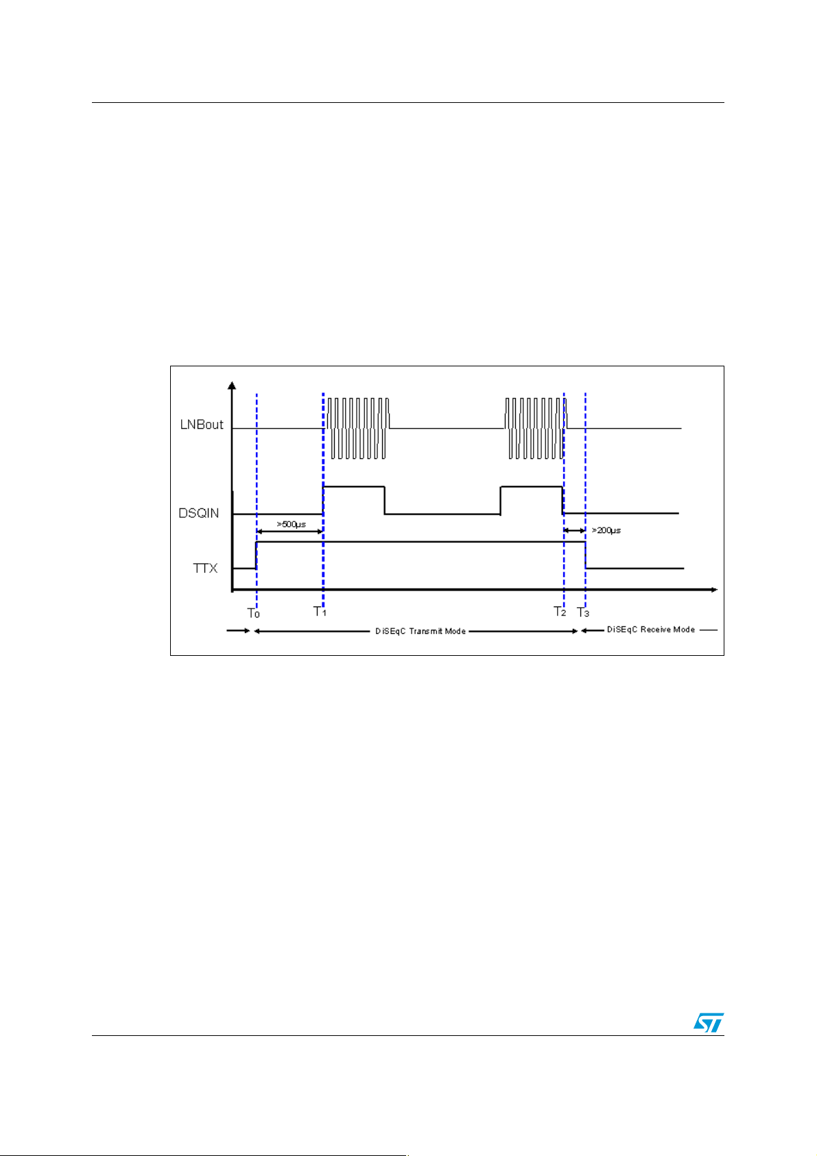
1.6 DiSEqC communication
The following steps must be taken to ensure the correct implementation of the DiSEqC 2.0
communication:
● T0: before starting the DiSEqC transmission, the TTX function must be activated
(through the TTX pin or TTX I
● T1: after a 500 µs minimum, the IC is ready to receive the DiSEqC code through the
DSQIN pin (or, alternatively, the TEN I
22 kHz burst).
● T2: when the transmission has elapsed, the TTX function must be set to LOW (through
the TTX pin or TTX I
2
C bit) not earlier than 200 µs after the last falling edge of the
DiSEqC code.
Figure 3. DiSEqC timing control
2
C bit).
2
C bit can be set to HIGH to activate the
1.7 Linear post-regulator, modulator and protection
The output voltage selection and the current selection commands join this block, which
manages all the LNB output function. This block gives feedback to the I
diagnostic block, regarding the status of the thermal protection, overcurrent protection and
output settings.
8/40 Doc ID 14431 Rev 1
2
C interface, from the
AN2713 Pin description
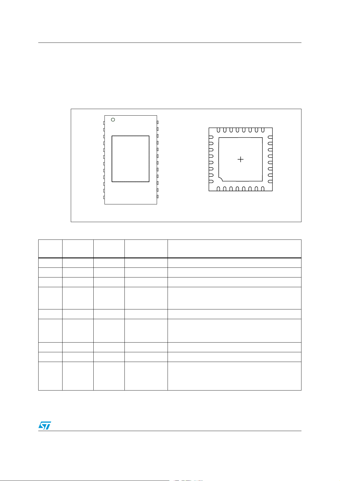
2 Pin description
The LNBH23 is available in exposed pad PowerSSO-24 or QFN32 packages for surface
mount assembly. Figure 4 shows the device pinouts for each package. Tabl e 1 briefly
summarizes the pin functionality.
Figure 4. LNBH23 pin configuration
.#
$%4).
$%4).
6#42,
6#42,
.#
.#
.#
.#
.#
.#
,8
,8
0' . $
0' . $
3$!
3$!
3#,
3#,
!$$2
!$$2
$31/54
$31/54
$31).
$31).
.#
)3
)3
%,
%,
650
650
.#
.#
6O48
6O48
6O28
6O28
!' .$
!' .$
6##
6##
6##,
6##,
"90
"90
448
448
%84-
%84-
Table 1. LNBH23 pin description
Pin n°
QFN32
19 17 V
18 16 V
4 6 Lx NMOS drain Integrated N-channel power MOSFET drain
27 22 V
21 19 V
22 20 V
6 8 SDA Serial data Bi-directional data from/to I
9 9 SCL Serial clock Clock from I
12 12 DSQIN DiSEqC input
Pin n°
PSSO-24
Symbol Name Pin Function
0OWER33/TOPVIEW
CC
–L Supply input 8 to 15 V analog power supply
CC
Supply input 8 to 15 V IC DC-DC power supply
1&.BOTTOMVIEW
Input of the linear post-regulator. The voltage on this pin
UP
Step-up voltage
is monitored by the internal step-up controller to keep a
minimum dropout across the linear pass transistor
oRX
LDO output port Output of the integrated linear post-regulator
Output port for
oTX
22 kHz
TX output to the LNB
tone TX
2
C bus
This pin accepts the DiSEqC code from the main
microcontroller. The LNBH23 uses this code to modulate
the internally-generated 22 kHz carrier. Set this pin to
ground if not used
2
C bus
!-V
Doc ID 14431 Rev 1 9/40

Pin description AN2713
Table 1. LNBH23 pin description (continued)
Pin n°
QFN32
14 14 TTX TTX enable
Pin n°
PSSO-24
Symbol Name Pin Function
2
This pin, as well as the TTX I
C bit of the system register,
is used to control the TTX function enable before starting
the 22 kHz tone transmission. Set this pin to ground if not
used
29 1 DETIN
Tone decoder
input
22 kHz tone decoder input, must be AC coupled to the
DiSEqC 2.0 bus
Open drain output of the tone detector to the main
11 11 DSQOUT DiSEqC output
microcontroller for DiSEqC 2.0 data decoding. It is low
when a tone is detected on the DETIN pin
External modulation logic input pin which activates the 22
kHz tone output on the VoTX pin. Set to ground if not
used
13 13 EXTM
External
modulation
5 7 P-GND Power ground DC-DC converter power ground
20 18 A-GND Analog ground Analog circuits ground
Needed for internal preregulator filtering. The BYP pin is
15 15 BYP Bypass capacitor
intended only to connect an external ceramic capacitor.
Any connection of this pin to external current or voltage
sources may cause permanent damage to the device
2
C bus addresses available by setting the address
10 10 ADDR Address setting
Two I
pin level voltage
28 23 ISEL Current selection
30 2 VCTRL
Output voltage
control
The resistor “R
defines the linear regulator current limit threshold with the
equation: Imax(typ.)=10000/R
13 V - 18 V linear regulator V
used only with VSEL=1. If VCTRL=1 or floating V
V (or 19.5 V if LLC=1). If VCTRL=0 then V
” connected between I
SEL
oRX switch control. To be
and GND
SEL
SEL
oRX
=18.5
oRX
=13.4 V
(LLC=either 0 or 1)
On the bottom side of the PowerSSO-24 package. Must
ePad ePad ePad ePad
be connected with power ground and to the ground layer
through vias to dissipate heat
10/40 Doc ID 14431 Rev 1
AN2713 Component selection guidelines
3 Component selection guidelines
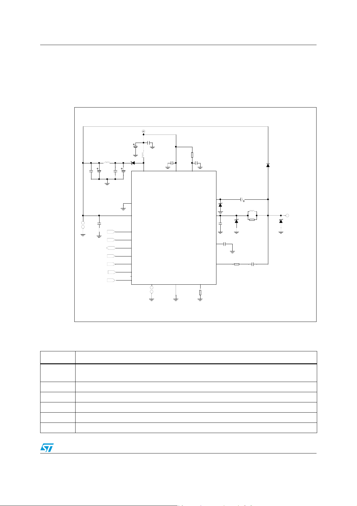
The LNBH23 application schematic in Figure 5 shows the typical configuration for a single
LNB power supply.
Figure 5. LNB power supply schematic using the LNBH23
6
#
±&
40
6UP
&ERRITE
"EAD
#
±&
±&
#
.#
±&
#
0OWER
#
$
3403!
±&
#
0'.$
6UP
6#42,
3#,
$31/54
$31).
%84-
448
,8
,,
±(
!$$2
#
±&
#
±&
,."(
6CC
2
6CC,
)3%,!'.$
#
±&
6O48
6O28
"90!33
$%4).3$!
$
"!4
#
±&
#
±&
$
"!4
2
+OHM
#
±&
,
±(
2
$
.
/HM
#
N&
,."/UTPUT
6O28
463
2
+!)OUT
23%,
Note: TVS diode to be used if surge protection is required (see Section 3.9).
Table 2. LNBH23 demonstration board BOM list
Component Notes
IC1
C1 100 µF 35 V electrolytic capacitor, higher value is suitable
C3, C5 100 µF 25 V electrolytic capacitor, ESR in the 150 mΩ to 350 mΩ range (see Section 3.3)
C9 10 µF 35 V electrolytic capacitor
C2, C7 0.1 µF 35 V ceramic capacitors
C4, C6 0.47 µF 35 V ceramic capacitors
LNBH23 PSSO-24 ePad for STEVAL-CBL003V1
LNBH23 QFN32 ePad for STEVAL-CBL005V1
Doc ID 14431 Rev 1 11/40
!-V

Component selection guidelines AN2713
Table 2. LNBH23 demonstration board BOM list (continued)
Component Notes
C8, C10,
C11
0.22 µF 35 V ceramic capacitors
C12 0.01 µF 35 V ceramic capacitor
R1 100 Ω 1/4 W resistor
R2 (R
)11 kΩ 1/16 W resistor (see Section 3.6)
SEL
R3 10 kΩ 1/4 W resistor
R4 15 Ω 1/4 W resistor
D1 STPS130A or similar Schottky diode (see Section 3.4)
D2, D4
BAT43 BAT43 (or Schottky diode with I
F(AV)
>0.2 A, V
1N5818
>25 V) or BAT30, BAT54, TMM BAT43,
RRM
D3 1N4007
L1 22 µH Inductor with Isat>I
L2
Ferrite bead filter; recommended part numbers: Panasonic EXCELS A35, Murata BL01RN1-A62 or
equivalent with similar or higher impedance and current rating higher than 2 A (see Section 3.2)
(see Section 3.5)
PEAK
L3 220 µH inductor with current rating higher than rated output current
TVS
LNBTVS22-XX TVS protection diode is recommended. Other solutions can be used depending on
the level of surge protection required (see Section 3.9)
3.1 Input capacitors
An electrolytic bypass capacitor (C1 in Figure 5) between 100 µF and 470 µF located close
to the LNBH23 is needed for stable operation. In any case, a ceramic capacitor between 100
nF and 470 nF is recommended to reduce the switching noise at the input voltage pin.
3.2 Ferrite bead
The most important parameter when selecting the ferrite bead is the rated current. Ensure
that the ferrite has a current rating of at least 2 A and impedance higher than 60 Ω at 100
MHz.
3.3 DC-DC converter output capacitors
Two low-cost electrolytic capacitors are needed on the DC-DC converter output stage (C3
and C5 in Figure 5). Moreover, two ceramic capacitors are recommended to reduce high
frequency switching noise. The switching noise is due to the voltage spikes of the fast
switching action of the output switch, and to the parasitic inductance of the output
capacitors. To minimize these voltage spikes, special low-inductance ceramic capacitors
can be used, and their lead lengths must be kept short and as close as possible to the IC
pins (C4 and C6 in Figure 5). To further reduce switching noise, a ferrite bead is
recommended between the capacitors (see Section 3.2 for required rating and impedance).
12/40 Doc ID 14431 Rev 1

AN2713 Component selection guidelines
The most important parameter for the output capacitors is the effective series resistance
(ESR). The DC-DC converter control loop circuit has been designed to work properly with
low-cost electrolytic capacitors which have ESR in the range of 200 mΩ. A 100 µF output
filter capacitor with ESR between 150 mΩ and 350 mΩ is a good choice in most application
conditions. It is also possible to use electrolytic capacitors up to 220 µF with ESR between
100 mΩ and 300 mΩ. The capacitor voltage rating must be at least 25 V, but if the highest
voltage selection condition is used (AUX=1), 35 V or higher voltage capacitors are
suggested.
3.4 DC-DC converter Schottky diode
In typical application conditions it is beneficial to use a 1 A Schottky diode which is suitable
for the LNBH23 DC-DC converter. Taking into consideration that the DC-DC converter
Schottky diode must be selected depending on the application conditions (V
N-channel Schottky diode like the STPS130A is recommended.
> 25 V), an
RRM
The average current flowing through the Schottky diode is lower than I
and can be
PEAK
calculated using Equation 1. In worst-case conditions, such as low input voltage and higher
output current, a Schottky diode capable of supporting the I
should be selected. I
PEAK
PEAK
can be calculated using Equation 2.
Equation 1
Vout
Id Iout
------------ -
⋅=
Vin
Table 3. Recommended Schottky diode
Vendor Part number IF(av) VF(max)
1N5818 1 A 0.50 V
1N5819 1 A 0.55 V
STPS130A 1 A 0.46 V
STMicroelectronics
STPS1L30A 1 A 0.30 V
STPS2L30A 2 A 0.45 V
1N5822 3 A 0.52 V
STPS340 3 A 0.63 V
STPS3L40A 3 A 0.5 V
3.5 DC-DC converter inductor
The LNBH23 operates with a standard 22 µH inductor for the entire range of supply voltages
and load current. The inductor saturation current rating (where inductance is approximately
70% of zero current inductance) must be greater than the switch peak current (I
calculated at:
● maximum load (Iout
● minimum input voltage (Vin
● maximum DC-DC output voltage (VUP
max
)
PEAK
)
)
min
=Vout
max
Doc ID 14431 Rev 1 13/40
+0.75 V)
max

Component selection guidelines AN2713
In this condition the switch peak current is calculated using the formula in Equation 2.
Equation 2
Ipeak
VUP
----------------------------------------------- -
⋅
max
⋅
Eff Vin
Iout
min
max
Vin
-----------------
+=
min
2LF
Vin
----------------------–
VUP
min
max
⎛⎞
1
⎝⎠
where
● Eff is the efficiency of the DC-DC converter (93% typ. at highest load)
● L is the inductance (22 µH typ.)
● F is the PWM frequency (220 kHz typ.).
Example:
Application conditions:
● Vout
● Vin
● Vup
● Iout
● Eff=90%
Based on Equation 2 and the preceding application conditions, I
= 19.2 V (supposing EN=VSEL=1, LLC=0)
max
= 11 V
min
=Vout
max
= 500 mA
max
max+Vdrop
= 19.2 V+0.75 V= 19.95 V
PEAK
is:
Equation 3
Ipeak
19.95 0.5⋅
---------------------------
0.9 11⋅
---------------------------------------------------------- -
22210
⋅⋅ ⋅ ⋅
11
6–
220 10
11
⎛⎞
1
-------------- -–
3
⎝⎠
19.95
1.52 A=+=
Several inductors suitable for the LNBH23 are listed in theTabl e 4 , although there are many
other manufacturers and devices that can be used. Consult each manufacturer for more
detailed information and for their entire selection of related parts, since many different
shapes and sizes are available. Ferrite core inductors should be used to obtain the best
efficiency. Choose an inductor that can handle at least the I
current without saturating,
PEAK
and ensure that the inductor has a low DCR (copper wire resistance) to minimize power
losses and, consequently, to maximize total efficiency.
Table 4. Recommended inductors
Vendor Part number Isat(A) DRC (mΩ) Mounting type
Sumida
CD104-220MC
RHC110-220M
822LY-220K
To ko
824LY-220K
A671HN-220L
A814LY-220M
1.6
2.4
1.3
1.72
2.44
2.0
67
88
70
76
21
75
SMD
Through-hole
Through-hole
Through-hole
Through-hole
SMD
14/40 Doc ID 14431 Rev 1

AN2713 Component selection guidelines
Table 4. Recommended inductors (continued)
Vendor Part number Isat(A) DRC (mΩ) Mounting type
Panasonic
ELC08D220E
ELC10D220E
DC1012-223
Coilcraft
PVC-0-223-03
DO3316P-223
3.6 Output current limit-R
selection
SEL
The linear regulator current limit threshold can be set through an external resistor connected
to ISEL pin. The resistor value defines the output current limit using the equation:
Equation 4
Imax A()
where R
is the resistor connected between the ISEL pin and GND. The highest
SEL
selectable current limit threshold is 1.0 A (typ) with R
3.7 Undervoltage diode protection
During a short-circuit removal on the LNB output, negative voltage spikes may occur on the
V
and V
oTx
between those pins and GND (see D2 and D4 in Figure 5).
pins. To prevent reliability problems, two low-cost Schottky diodes are used
oRx
1.8
3.2
2.5
3
2.6
10000
----------------=
R
SEL
SEL
=10 kΩ.
51
40
46
35
85
Through-hole
Through-hole
Through-hole
Through-hole
SMD
3.8 DiSEqC implementation and inductor selection
To comply with DiSEqC 2.x requirements, an output R-L filter is needed. The 22 kHz tone
transmission occurs through the V
pin. The V
function must be activated only during the tone transmission while the V
oTX
provides the 13/18 V output voltage. This solution allows the 22 kHz tone to pass without
any losses due to the R-L filter impedance. But to respect the minimum DC voltage
requirement, it is recommended to use an inductor with a current rating higher than the rated
output current and a low DRC to minimize the voltage drop.
For example, supposing:
● Iout = 500 mA
● DRC=51 mΩ (Panasonic inductor ELC08D221E)
Equation 5
Vdrop V() DCR Ω()Iout A() 0.051 0.5 0.025 V=⋅=⋅=
Several inductors suitable for the LNBH23 are listed in the Ta bl e 5 .
Doc ID 14431 Rev 1 15/40
pin, whereas the DC voltage is provided from the V
oTX
oRX
oRx

Component selection guidelines AN2713
Table 5. Recommended inductors for output R-L filter
Vendor Part number Isat(A) DRC(mΩ) Mounting type
Sumida
To ko
Panasonic
Coilcraft
3.9 TVS diode
The LNBH23 device is directly connected to the antenna cable in a set-top box. Atmospheric
phenomenon can cause high voltage discharges on the antenna cable causing damage to
the attached devices. Surge pulses occur due to direct or indirect lightning strikes to an
external (outdoor) circuit. This leads to currents or electromagnetic fields causing high
voltage or current transients. LNBH23 devices are not able to withstand such high energy
discharges, so transient voltage suppressor (TVS) devices are used to protect the LNBH23
and other devices electrically connected to the antenna cable.
CD104-221MC
RHC110-221M
822LY-221K
824LY-221K
A671HN-221L
A814LY-221M
ELC08D221E
ELC10D221E
DC1012-223
PVC-0-223-03
DO3316P-223
1.6
2.4
1.3
1.72
2.44
2.0
1.8
3.2
2.5
3
2.6
67
88
70
76
21
75
51
40
46
35
85
SMD
Through-hole
Through-hole
Through-hole
Through-hole
SMD
Through-hole
Through-hole
Through-hole
Through-hole
SMD
The LNBTVS developed by STMicroelectronics is a dedicated lightning and electrical
overstress surge protection device for LNB voltage regulators. These protection devices are
designed to comply with the stringent IEC 61000-4-5 standards and to withstand surges of
up to 500 A. ST offers a broad selection of these products for cost/performance
optimization.
The selection of the TVS diode must be made based on the maximum peak power
dissipation that the diode is capable of supporting.
Table 6. Recommended LNBTVS
Vendor Part number VBR
LNBTVS4-220 23.1 1800
LNBTVS4-221 23.1 2000
STMicroelectronics
LNBTVS4-222S 23.1 2000
LNBTVS6-221S 21.3 3000
Select the TVS diode which is capable of supporting the required Ppp(W) value indicated in
(V) Ppp(W)10/100µs
TYP
Ta bl e 6 .
16/40 Doc ID 14431 Rev 1

AN2713 Other application circuits
4 Other application circuits
The following paragraphs present two particular application solutions: the first can be used
to reduce the 18 V to 13 V transition time, while the second is designed to improve lightning
surge protection.
4.1 18 V to 13 V fast transition with high bus capacitance
In cases of very high bus capacitance (Cbus>10 µF) and very low output current, an
external circuit (with a 4.7 V Zener diode and a 100 Ω series resistor) can be added to
reduce 18 V to 13 V transition fall time, as shown in Figure 6.
Figure 6. External circuit to reduce 18 V to 13 V fall time transition
The TTX bit (or pin) must be set high only during the transition from 18 V to 13 V. The TTX
function activates only the push-pull circuit, but not the tone output. The 22 kHz tone is
activated only when the TEN bit (or DSQIN pin) is also set high and injected into the LNB
bus through the 10 µF capacitor.
When the TTX function is activated, the V
Vout (for example, if Vout=18 V then V
voltage is internally set at 5 V (typ). below the
oTx
=18-5=13 V) and, at the same time, the P-channel
oTx
is enabled to sink current (note: the P-channel is internally current-limited).
With a 4.7 V Zener diode, when TTX=high, the current through the Zener is: Iz=(5-
4.7)/100=3 mA. If TTX=low, the current through the Zener is negligible.
If there is a high output capacitance present, during the transition from 18 V to 13 V (with
TTX=high), the voltage drop (Vout-V
level (at 13 V-5 V=8 V) and, consequently, the Zener current is also increased until the
output capacitance is discharged to 13 V. For example, with 100 µF on the output, the 18 V
) is increased because the V
oTx
goes quickly to low
oTx
to 13 V fall time is about 25 ms.
Doc ID 14431 Rev 1 17/40

Other application circuits AN2713
The following steps must be taken to ensure the correct implementation of 18 to 13 V
transition with the V
● T0: to start the 18 V to 13 V transition the TTX function must be activated at least
0.5 ms before setting the VSEL I
● T1: set LOW VSEL I
● T2: after 30 ms, 18 V to 13 V LNB transition time is elapsed at T2. The 30 ms delay is
addition circuit shown in Figure 6:
oTx
2
C bit (set HIGH TTX I2C bit or TTX pin).
2
C bit.
valid to ensure 18 V to 13 V complete transition in case of Cbus=100 µF and
Iout=0 mA. The delay time can be modified with different Cbus capacitance and output
current value.
Figure 7. Fast transition timing sequence
18/40 Doc ID 14431 Rev 1

AN2713 Other application circuits
Figure 8. Fast transition timing control with 22 kHz tone
If the internal 22 kHz tone generator is activated (TEN I
T1 set low the VSEL I
2
C bit or VCTRL pin and after 25 ms, 18 V to 13 V LNB transition time
2
C bit or DSQIN pin is set high), at
is elapsed at T2.
4.2 Reverse voltage and lightning surge protection
Figure 9 shows a suggested schematic to improve output circuit protection in applications
where:
● TVS diode with Vclamp voltage of 25 V is required
● an external power supply source could force a reverse DC voltage of 25 V on the LNB
bus
Doc ID 14431 Rev 1 19/40

Other application circuits AN2713
Figure 9. External circuit protection schematic
!-V
The Schottky diode prevents the reverse voltage from flowing into the V
pin (internally
oRx
connected to the linear regulator). In applications where a reverse DC voltage (up to 60 V) is
forced and low Vout tolerance is required, the recommended part number is STPS3L60U. In
any case, it is possible to use a different part based to the DC reverse voltage. D3 shields
the V
pin because it discharges the reverse voltage into the Vup capacitor and D4c
oTx
(suggested part number SM2T18A) is mandatory for DC reverse voltage ≥ 25 V.
20/40 Doc ID 14431 Rev 1
AN2713 Layout guidelines
5 Layout guidelines
Due to high current levels and fast switching waveforms, which radiate noise, a proper
printed circuit board (PCB) layout is essential. Sensitive analog grounds can be protected by
using a star ground configuration. Also, lead lengths should be minimized to reduce stray
capacitance, trace resistance, and radiated noise. Ground noise can be minimized by
connecting GND, the input bypass capacitor ground lead, and the output filter capacitor
ground lead to a single point (star ground configuration). Place input bypass capacitors (C1,
C2, C7 and C8) as close as possible to Vcc and GND, and the DC-DC output capacitors
(C3, C4, C5 and C6) as close as possible to VUP. Excessive noise at the Vcc input may
falsely trigger the undervoltage circuitry, resetting the I
the registers are set to zero and the LNBH23 is put into shutdown mode.
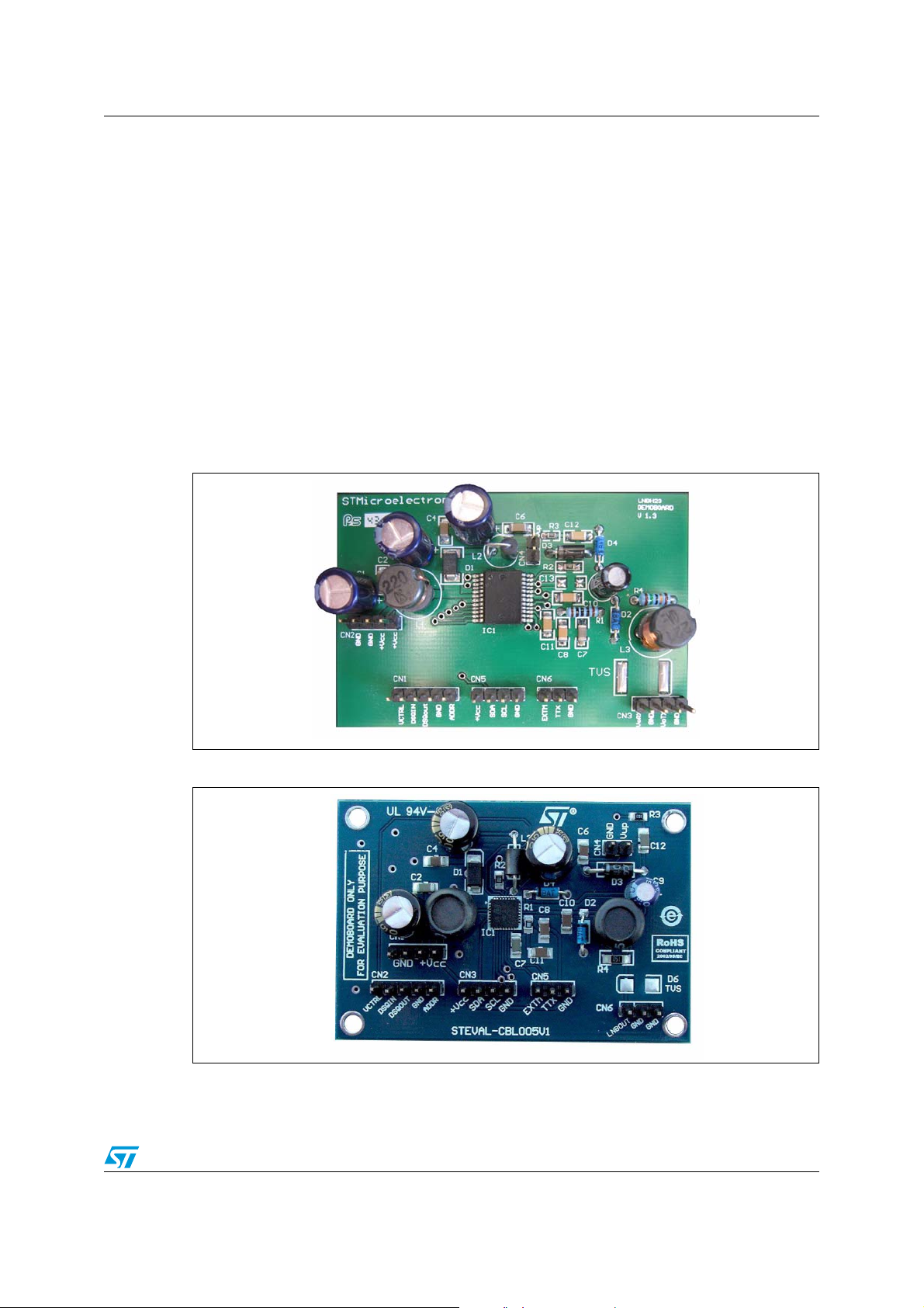
LNB power supply demonstration boards are available for each package option through
order codes STEVAL-CBL003V1 (Figure 10) and STEVAL-CBL005V1 (Figure 11).
Figure 10. STEVAL-CBL003V1 demonstration board photo (PowerSSO-24 package)
2
C internal registers. If this occurs,
Figure 11. STEVAL-CBL005V1 demonstration board photo (QFN32 package)
Doc ID 14431 Rev 1 21/40

Layout guidelines AN2713
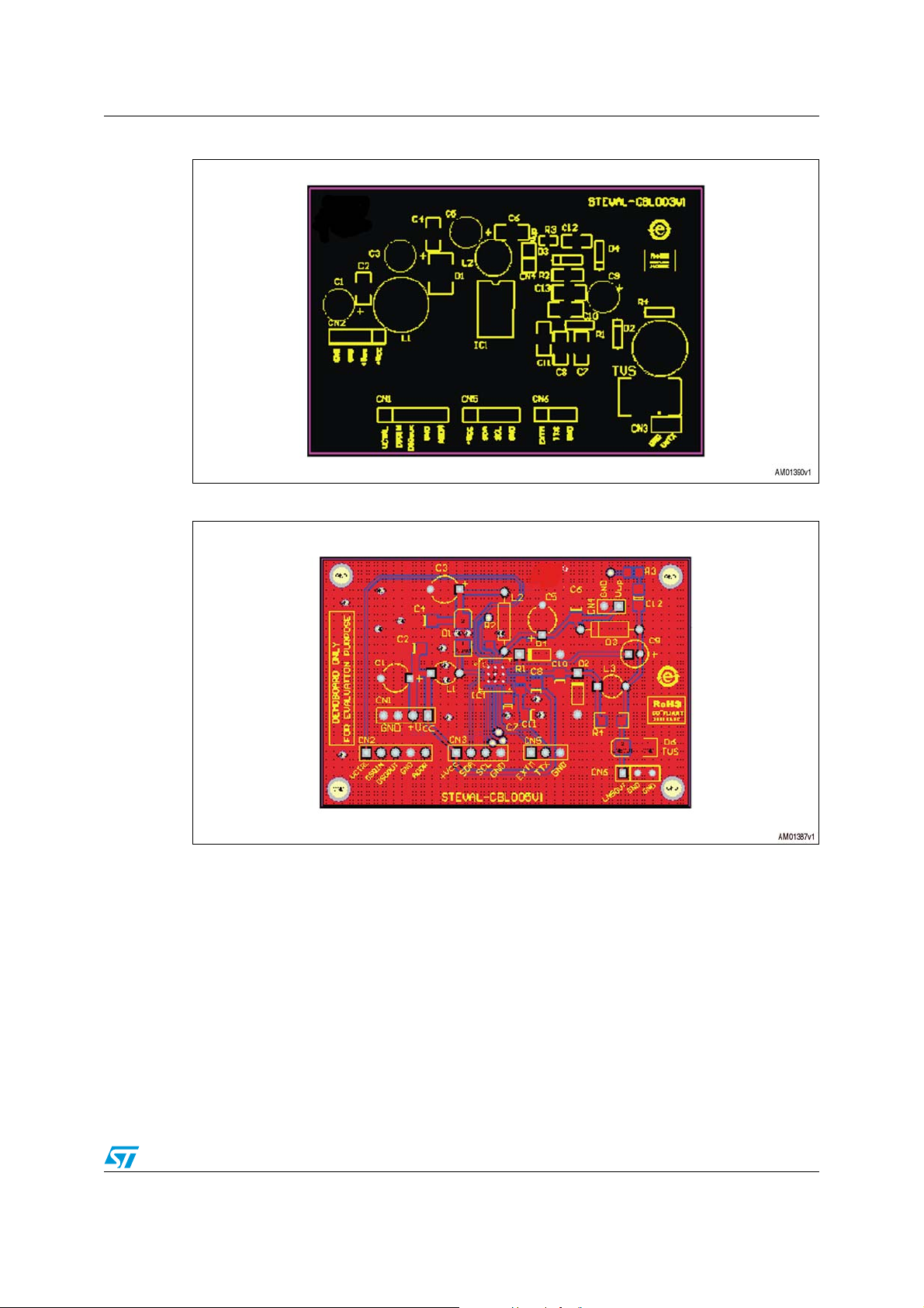
5.1 PCB layout
Any switch mode power supply requires a good PCB layout in order to achieve maximum
performance. Component placement, and GND trace routing and width are the major
issues. Basic rules commonly used for DC-DC converters for good PCB layout should be
followed.
All traces carrying current should be drawn on the PCB as short and as thick as possible.
This should be done to minimize resistive and inductive parasitic effects, and increase
system efficiency.
White arrows indicate the suggested PCB (ring) ground plane to avoid spikes on the output
voltage (this is related to the switching side of the LNBH23). Good soldering of the ePad
helps on this issue.
Figure 12. STEVAL-CBL003V1 PCB top layer
Figure 13. STEVAL-CBL003V1 PCB bottom layer
22/40 Doc ID 14431 Rev 1
AM01388v1
AN2713 Layout guidelines
Figure 14. STEVAL-CBL003V1 component layout
Figure 15. STEVAL-CBL005V1 PCB top layer
Doc ID 14431 Rev 1 23/40
Layout guidelines AN2713
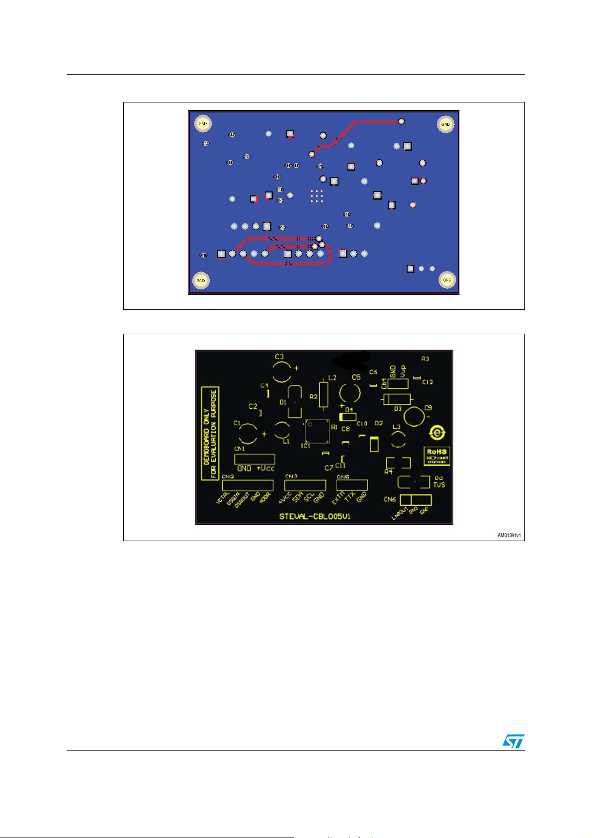
Figure 16. STEVAL-CBL005V1 PCB bottom layer
AM01389v1
Figure 17. STEVAL-CBL005V1 component layout
5.2 Startup procedure
Testing the demonstration board requires a PC with a parallel port (ECP printer port), an I2C
bus interface, software (LNBxxx control suite), a dual-output power supply (3 A clamp
current or higher) and an electronic load.
● Step 1: Install the LNBXXX control suite software (see Section 6).
● Step 2: Plug the I
● Step 3: Supply the demonstration board through CN2.
● Step 4: Refer to Section 6.1 of software installation guide to use the software.
24/40 Doc ID 14431 Rev 1
2
C connector into CN5.

AN2713 Layout guidelines
Figure 18. STEVAL-CBL003V1 connectors
CN2
To supply the demonstration
(Typ. 12 VDC) Use a power supply
with a 3 A clamp current or higher
CN1
:
ADDR tip
2
I
Connect ADDR pin to ground to set
C address = 02
board
CN5
2
I
C interface connections
For data transmissions from the I C
interface to the LNBH23 and vice-
versa. Care should be taken to ensure
proper connection of the I C interface
Figure 19. STEVAL-CBL005V1 connectors
CN
1
To supply the demo board
(Typ. 12 V DC) Use a power supply
with a 3 A clamp current or higher
CN3
To supply LNB
VoTX=Vout test point
:
2
2
AM01392v1
CN6
To supply LNB
VoTX=Vout test point
CN2
ADDR tip:Connect ADDR pin to ground to set
2
C address = 02
I
CN3
I2C interface connections
For data transmissions from I C
interface to the LNBH23 and vice-
versa.
Care should be taken to ensure
proper connection of the I C interface
:
2
AM01393v1
Doc ID 14431 Rev 1 25/40

Layout guidelines AN2713
Figure 20. STEVAL-CBL003V1 bench test
Volt #1
Power supply
A
V
D.U.T.= STEVAL-CBL003V1
D.U.T.
CN2
CN5
I2C interface
Figure 21. STEVAL-CBL005V1 bench test
Power supply
A
V
D.U.T.= STEVAL-CBL005V1
CN
3
Scope
AM01394v1
Volt #1
I2C
interface
26/40 Doc ID 14431 Rev 1
CN1
D.U.T.
CN3
CN
6
Scope
AM01395v1

AN2713 Software installation
6 Software installation
Unzip the compressed file and perform the installation by clicking on the SETUP.exe file.
Click on: Windows
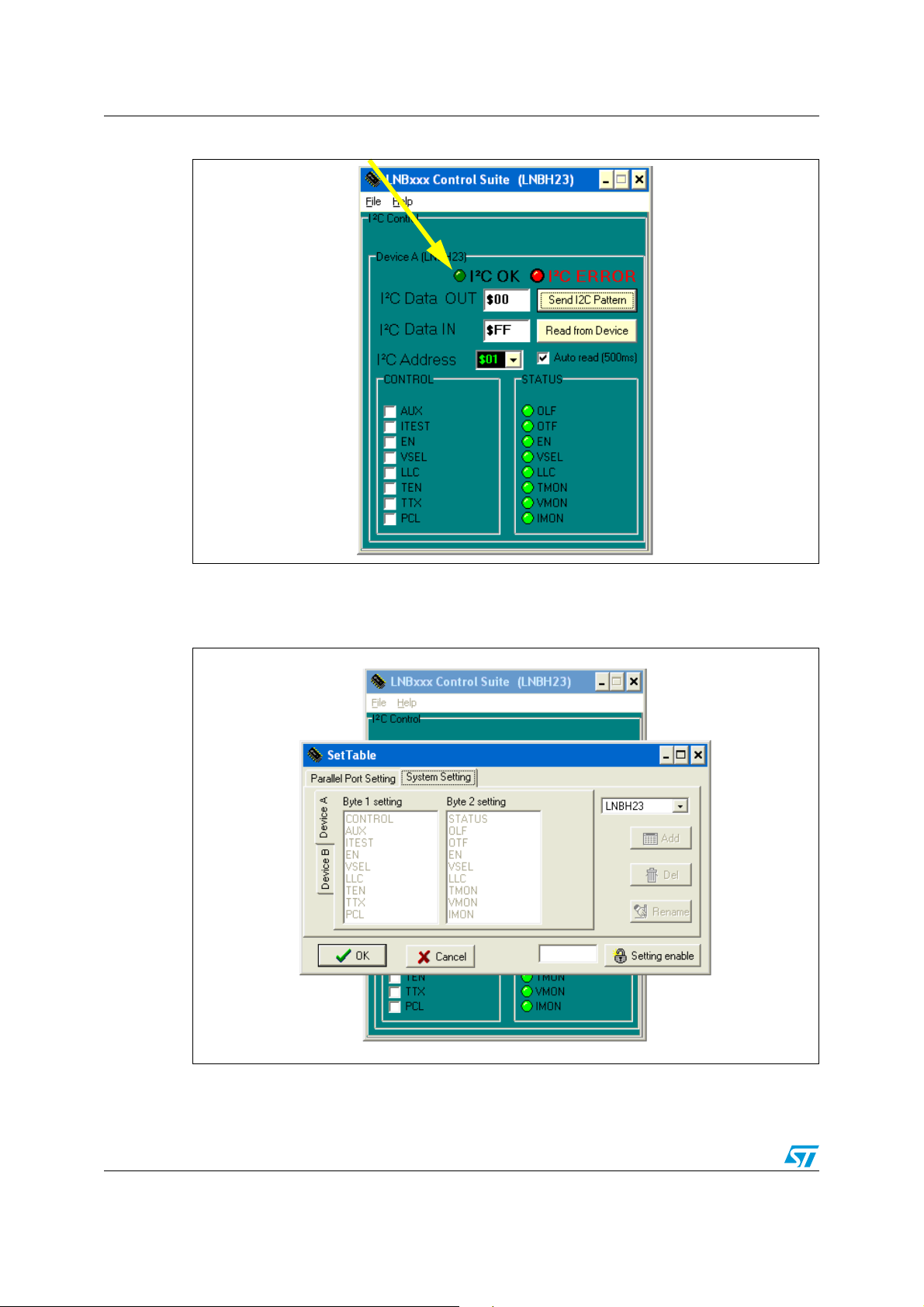
The screen shown in Figure 22 appears, with a green light indicating that the hardware and
software are ready to work.
®
“start” menu -> Program -> STMicroelectronics -> LNBxxx control suite.
Figure 22. PC to I
2
C main window
Click to send command
programmed in the
command window
Command window
The red "I
2
I
C cable (swap the SCL and SDA, if needed) and power supply need to be checked.
2
C ERROR" indicator signals that the LPT port needs to be configured, and/or the
Status window
Received bits from device
Doc ID 14431 Rev 1 27/40
Software installation AN2713
Figure 23. I2C bus communication error
The user can choose the device, printer port address for the PC and correct settings of the
SCL and SDA bits to customize the I
2
C hardware interface.
Figure 24. Main settings window
In the system setting menu, the device to be tested can be changed.
28/40 Doc ID 14431 Rev 1

AN2713 Software installation
Figure 25. Device selection window
From the parallel port setting menu, the LPT parameters can be set.
Figure 26. Parallel port setting
Doc ID 14431 Rev 1 29/40

Software installation AN2713
Figure 27. LPT1 setting
Setting for
LPT1
Figure 28. Password setting
“STM” is the
password
(case sensitive)
At this point, the device address can be chosen. For the LNBH23, only $02= ADDR pin force
to GND or $03= ADDR pin force to +5 V can be selected.
30/40 Doc ID 14431 Rev 1

AN2713 Software installation
Figure 29. I2C device address setting
To obtain the status of the received bits in real-time, the "Auto read" checkbox must be
checked.
Figure 30. Autoread setting
Doc ID 14431 Rev 1 31/40
Software installation AN2713
6.1 How to use the LNBH23 demonstration board with the LNBxxx control suite software
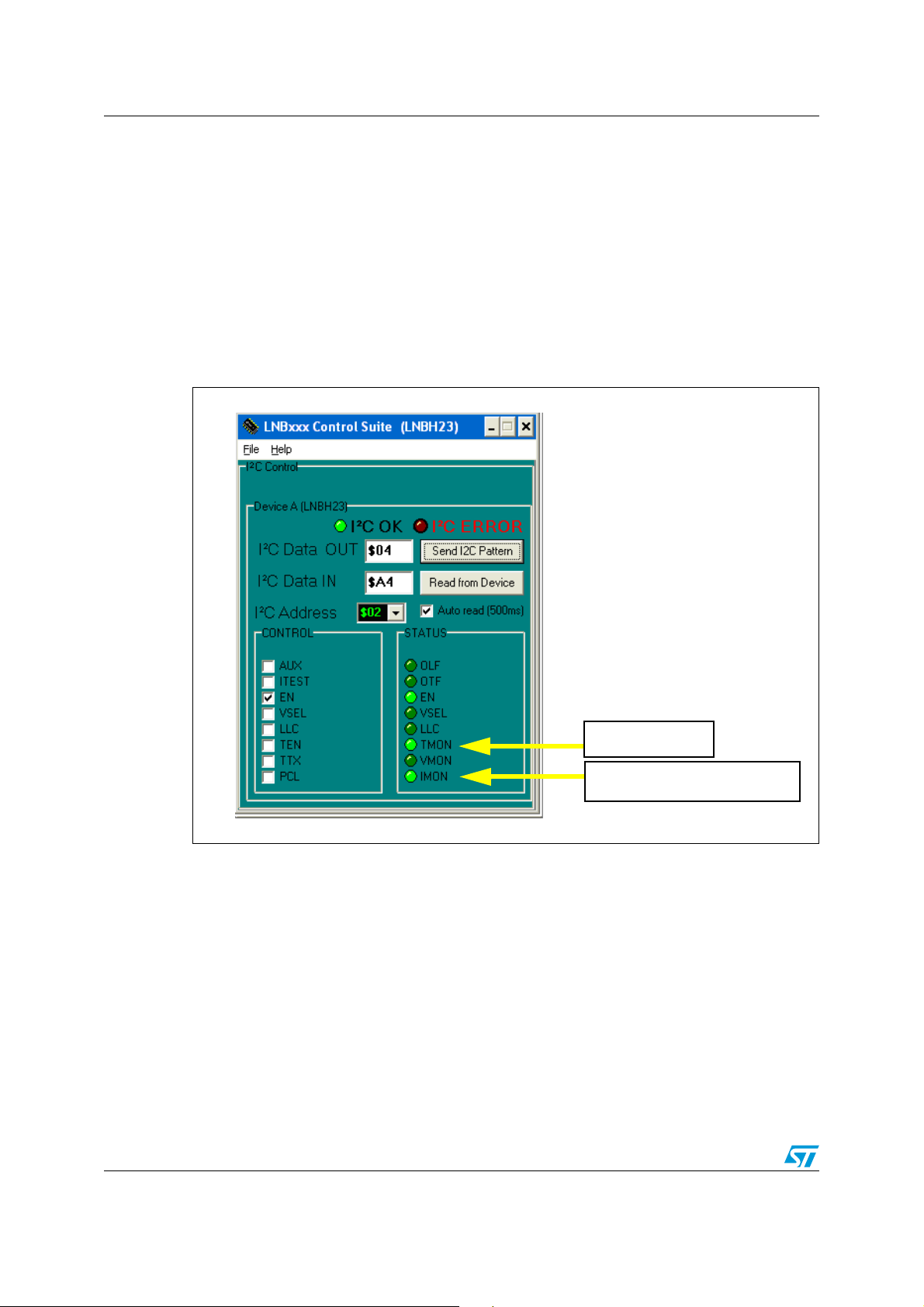
To power the IC, place a check in the EN checkbox and click the "Send I2C Pattern" button.
If the device accepts the command string, the green indicator turns on. If there is no
powerup after sending the command, it may be that the 12 V power supply is not sufficient
to start the application, and more current capability is needed.
The screenshot in Figure 31 shows the following conditions:
● EN=1=ON
● Vout=13.4 V
Figure 31. Power-on at 13.4 V
typ
A status light “on” for OLF, OTF, TMON, VMON and IMON indicates that an error has
occurred.
32/40 Doc ID 14431 Rev 1
Light on=22 kHz
tone absence
Light on=load less than 6 mA
(ITest=0) or 12 mA

AN2713 Software installation
The screenshot in Figure 32 shows the following conditions:
● EN=1, VSEL=1
● Vout=18.5 V
typ
Figure 32. Power-on at 18.5 V
Doc ID 14431 Rev 1 33/40

Software installation AN2713
The screenshot in Figure 33 shows the following conditions:
● EN=1, VSEL=1, LLC=1
● Vout=19.5 V
typ
Figure 33. LLC activation
34/40 Doc ID 14431 Rev 1

AN2713 Software installation
The screenshot in Figure 34 shows the following conditions:
● EN=1, TEN=TTX=1
● Vout=13.4 V
+ 22 kHz tone
typ
Figure 34. Tone activation
For 22 kHz tone, TEN and
TTX bits must be selected
Doc ID 14431 Rev 1 35/40

Software installation AN2713
Overload condition
If the OLF (overload flag) indicator is on, a fault condition on the output has been detected
and the status of this bit is changed. It turns off when the fault condition is removed.
● EN=1
● Vout=fault, OLF=1
Figure 35. Overload detection
Light on=overload flag
activated
Light on=Vout fault
The screenshot in Figure 36 shows the following conditions:
● EN=1
● Vout=fault, OTF=1
Figure 36. Overtemperature detection
Light on=overtemperature
flag activated
36/40 Doc ID 14431 Rev 1

AN2713 Software installation
If the PCL checkbox is checked, a simple output short-circuit current clamp is set. If not, the
overcurrent protection circuit works dynamically: as soon as an overload is detected, the
output current is provided for 90 ms (typ.), after which the output is set in shutdown for a
time TOFF of 900 ms (typ). Simultaneously, the diagnostic OLF I
2
C bit of the system register
is set high. This feature allows the reduction of the total power dissipation during an
overload or a short-circuit condition:
● EN=1, PCL=1
● Vout=13.4 V
typ
Figure 37. PCL deactivation
Doc ID 14431 Rev 1 37/40

Software installation AN2713
The AUX bit can be set high to force the LNBH23 output voltage to the highest voltage on
the line (22 V typ.) during the minimum current diagnostic phase, in order to detect the
output load and check the dish status or any optional devices inserted on the line.
The maximum current detected at ITEST=0 is 6 mA, while at ITEST=1 it is 12 mA.
During the minimum diagnostic current test, setting only EN=ITEST=AUX=1 is
recommended. The screenshot in Figure 38 shows the following conditions:
● EN=1, AUX=1
● Vout=22 V (for testing multiswitch-box dish connection)
Figure 38. AUX activation
38/40 Doc ID 14431 Rev 1

AN2713 Revision history
7 Revision history
Table 7. Document revision history
Date Revision Changes
13-Nov-2009 1 Initial release.
Doc ID 14431 Rev 1 39/40

AN2713
Please Read Carefully:
Information in this document is provided solely in connection with ST products. STMicroelectronics NV and its subsidiaries (“ST”) reserve the
right to make changes, corrections, modifications or improvements, to this document, and the products and services described herein at any
time, without notice.
All ST products are sold pursuant to ST’s terms and conditions of sale.
Purchasers are solely responsible for the choice, selection and use of the ST products and services described herein, and ST assumes no
liability whatsoever relating to the choice, selection or use of the ST products and services described herein.
No license, express or implied, by estoppel or otherwise, to any intellectual property rights is granted under this document. If any part of this
document refers to any third party products or services it shall not be deemed a license grant by ST for the use of such third party products
or services, or any intellectual property contained therein or considered as a warranty covering the use in any manner whatsoever of such
third party products or services or any intellectual property contained therein.
UNLESS OTHERWISE SET FORTH IN ST’S TERMS AND CONDITIONS OF SALE ST DISCLAIMS ANY EXPRESS OR IMPLIED
WARRANTY WITH RESPECT TO THE USE AND/OR SALE OF ST PRODUCTS INCLUDING WITHOUT LIMITATION IMPLIED
WARRANTIES OF MERCHANTABILITY, FITNESS FOR A PARTICULAR PURPOSE (AND THEIR EQUIVALENTS UNDER THE LAWS
OF ANY JURISDICTION), OR INFRINGEMENT OF ANY PATENT, COPYRIGHT OR OTHER INTELLECTUAL PROPERTY RIGHT.
UNLESS EXPRESSLY APPROVED IN WRITING BY AN AUTHORIZED ST REPRESENTATIVE, ST PRODUCTS ARE NOT
RECOMMENDED, AUTHORIZED OR WARRANTED FOR USE IN MILITARY, AIR CRAFT, SPACE, LIFE SAVING, OR LIFE SUSTAINING
APPLICATIONS, NOR IN PRODUCTS OR SYSTEMS WHERE FAILURE OR MALFUNCTION MAY RESULT IN PERSONAL INJURY,
DEATH, OR SEVERE PROPERTY OR ENVIRONMENTAL DAMAGE. ST PRODUCTS WHICH ARE NOT SPECIFIED AS "AUTOMOTIVE
GRADE" MAY ONLY BE USED IN AUTOMOTIVE APPLICATIONS AT USER’S OWN RISK.
Resale of ST products with provisions different from the statements and/or technical features set forth in this document shall immediately void
any warranty granted by ST for the ST product or service described herein and shall not create or extend in any manner whatsoever, any
liability of ST.
ST and the ST logo are trademarks or registered trademarks of ST in various countries.
Information in this document supersedes and replaces all information previously supplied.
The ST logo is a registered trademark of STMicroelectronics. All other names are the property of their respective owners.
© 2009 STMicroelectronics - All rights reserved
STMicroelectronics group of companies
Australia - Belgium - Brazil - Canada - China - Czech Republic - Finland - France - Germany - Hong Kong - India - Israel - Italy - Japan -
Malaysia - Malta - Morocco - Philippines - Singapore - Spain - Sweden - Switzerland - United Kingdom - United States of America
www.st.com
40/40 Doc ID 14431 Rev 1
 Loading...