

Page 1

AN2708
Application note
2X36 W digital dimmable ballast with L6574 and ST7FDALI
Introduction
This document describes a high-efficiency, high power factor, low THD and digital dimming
electronic ballast designed to drive 2X36 W T8 tube lamps.
The system consists of three main blocks:
The high-frequency ballast includes an active power factor correction circuit based on the
L6562 for universal input voltage as well as a ballast control circuit based on the L6574. The
digital dimming is performed by interfacing the ST7FDALI microcontroller with the analog
half-bridge driver.
The DALI control unit is dedicated to address the slaves, to display the lamp status and to
send the dimming commands. This unit is provided with a keyboard which allows setting
different dimming scenes over a wide range (5-100%) as well as putting in standby and
restarting the ballast. The DALI communication protocol includes single and group mode, as
well as broadcast mode to address the slaves.
The AC-DC adapter is based on the VIPer12A-E. This is an offline double-output isolated
power supply in DCM flyback configuration. The outputs are set for 20 V to supply the
communication bus and for 5 V to supply the MASTER microcontroller.
The three blocks are described in detail and their performances are shown. In addition some
of DALI basics are explained.
March 2008 Rev 1 1/42
www.st.com
Page 2

Contents AN2708
Contents
1 Block diagram and system operating conditions . . . . . . . . . . . . . . . . . 5
2 High-frequency ballast . . . . . . . . . . . . . . . . . . . . . . . . . . . . . . . . . . . . . . . 7
2.1 PFC converter . . . . . . . . . . . . . . . . . . . . . . . . . . . . . . . . . . . . . . . . . . . . . 11
2.2 Half-bridge inverter and ballast . . . . . . . . . . . . . . . . . . . . . . . . . . . . . . . . 14
2.2.1 Lamp dimming . . . . . . . . . . . . . . . . . . . . . . . . . . . . . . . . . . . . . . . . . . . . 16
2.2.2 Supply section . . . . . . . . . . . . . . . . . . . . . . . . . . . . . . . . . . . . . . . . . . . . 17
2.2.3 Lamp turn-on and lamp turn-off . . . . . . . . . . . . . . . . . . . . . . . . . . . . . . . 18
2.2.4 Verification of lamp status . . . . . . . . . . . . . . . . . . . . . . . . . . . . . . . . . . . 21
2.2.5 Ballast performances . . . . . . . . . . . . . . . . . . . . . . . . . . . . . . . . . . . . . . . 22
3 DALI master unit . . . . . . . . . . . . . . . . . . . . . . . . . . . . . . . . . . . . . . . . . . . 24
3.1 Master unit schematic and bill of material . . . . . . . . . . . . . . . . . . . . . . . . 26
4 Basics of DALI . . . . . . . . . . . . . . . . . . . . . . . . . . . . . . . . . . . . . . . . . . . . . 29
5 DALI master AC-DC adapter . . . . . . . . . . . . . . . . . . . . . . . . . . . . . . . . . . 32
5.1 Adapter description . . . . . . . . . . . . . . . . . . . . . . . . . . . . . . . . . . . . . . . . . 32
5.2 Adapter bill of material . . . . . . . . . . . . . . . . . . . . . . . . . . . . . . . . . . . . . . . 35
5.3 Adapter performances . . . . . . . . . . . . . . . . . . . . . . . . . . . . . . . . . . . . . . . 36
5.3.1 Steady state tests . . . . . . . . . . . . . . . . . . . . . . . . . . . . . . . . . . . . . . . . . 36
5.3.2 Startup behavior . . . . . . . . . . . . . . . . . . . . . . . . . . . . . . . . . . . . . . . . . . 37
5.3.3 Dynamic load tests . . . . . . . . . . . . . . . . . . . . . . . . . . . . . . . . . . . . . . . . 38
5.3.4 Line regulation . . . . . . . . . . . . . . . . . . . . . . . . . . . . . . . . . . . . . . . . . . . . 39
5.3.5 Load regulation . . . . . . . . . . . . . . . . . . . . . . . . . . . . . . . . . . . . . . . . . . . 39
5.3.6 Efficiency variation . . . . . . . . . . . . . . . . . . . . . . . . . . . . . . . . . . . . . . . . . 40
5.3.7 Conducted emissions test . . . . . . . . . . . . . . . . . . . . . . . . . . . . . . . . . . . 40
6 References . . . . . . . . . . . . . . . . . . . . . . . . . . . . . . . . . . . . . . . . . . . . . . . . 41
7 Revision history . . . . . . . . . . . . . . . . . . . . . . . . . . . . . . . . . . . . . . . . . . . 41
2/42
Page 3

AN2708 List of tables
List of tables
Table 1. System operating conditions. . . . . . . . . . . . . . . . . . . . . . . . . . . . . . . . . . . . . . . . . . . . . . . . . 6
Table 2. Ballast-slave communication . . . . . . . . . . . . . . . . . . . . . . . . . . . . . . . . . . . . . . . . . . . . . . . . 8
Table 3. Ballast bill of material . . . . . . . . . . . . . . . . . . . . . . . . . . . . . . . . . . . . . . . . . . . . . . . . . . . . . . 8
Table 4. PFC operating conditions . . . . . . . . . . . . . . . . . . . . . . . . . . . . . . . . . . . . . . . . . . . . . . . . . . 12
Table 5. Power stage design equations . . . . . . . . . . . . . . . . . . . . . . . . . . . . . . . . . . . . . . . . . . . . . . 12
Table 6. L6562 biasing circuitry design equations . . . . . . . . . . . . . . . . . . . . . . . . . . . . . . . . . . . . . . 13
Table 7. Lamp parameters . . . . . . . . . . . . . . . . . . . . . . . . . . . . . . . . . . . . . . . . . . . . . . . . . . . . . . . . 14
Table 8. L6574 biasing circuitry design equations for operating conditions . . . . . . . . . . . . . . . . . . . 16
Table 9. Ballast performances . . . . . . . . . . . . . . . . . . . . . . . . . . . . . . . . . . . . . . . . . . . . . . . . . . . . . 23
Table 10. Master unit bill of material. . . . . . . . . . . . . . . . . . . . . . . . . . . . . . . . . . . . . . . . . . . . . . . . . . 27
Table 11. SMPS operating conditions . . . . . . . . . . . . . . . . . . . . . . . . . . . . . . . . . . . . . . . . . . . . . . . . 32
Table 12. Adapter bill of material . . . . . . . . . . . . . . . . . . . . . . . . . . . . . . . . . . . . . . . . . . . . . . . . . . . . 35
Table 13. Document revision history . . . . . . . . . . . . . . . . . . . . . . . . . . . . . . . . . . . . . . . . . . . . . . . . . 41
3/42
Page 4

List of figures AN2708
List of figures
Figure 1. System block diagram . . . . . . . . . . . . . . . . . . . . . . . . . . . . . . . . . . . . . . . . . . . . . . . . . . . . . 5
Figure 2. 2X36 W digital dimmable ballast with L6574 and ST7FDALI . . . . . . . . . . . . . . . . . . . . . . . . 6
Figure 3. Ballast schematic . . . . . . . . . . . . . . . . . . . . . . . . . . . . . . . . . . . . . . . . . . . . . . . . . . . . . . . . . 7
Figure 4. PFC performances at 230 V
Figure 5. Lamp ballast model. . . . . . . . . . . . . . . . . . . . . . . . . . . . . . . . . . . . . . . . . . . . . . . . . . . . . . . 14
Figure 6. Ballast transfer functions (magnitude) . . . . . . . . . . . . . . . . . . . . . . . . . . . . . . . . . . . . . . . . 15
Figure 7. DALI protocol brightness values . . . . . . . . . . . . . . . . . . . . . . . . . . . . . . . . . . . . . . . . . . . . . 17
Figure 8. Ballast controls timing chart . . . . . . . . . . . . . . . . . . . . . . . . . . . . . . . . . . . . . . . . . . . . . . . . 19
Figure 9. Idle state . . . . . . . . . . . . . . . . . . . . . . . . . . . . . . . . . . . . . . . . . . . . . . . . . . . . . . . . . . . . . . . 20
Figure 10. Turn-on procedure . . . . . . . . . . . . . . . . . . . . . . . . . . . . . . . . . . . . . . . . . . . . . . . . . . . . . . . 20
Figure 11. Turn-off procedure . . . . . . . . . . . . . . . . . . . . . . . . . . . . . . . . . . . . . . . . . . . . . . . . . . . . . . . 20
Figure 12. Forward frame timing . . . . . . . . . . . . . . . . . . . . . . . . . . . . . . . . . . . . . . . . . . . . . . . . . . . . . 21
Figure 13. Backward frame timing . . . . . . . . . . . . . . . . . . . . . . . . . . . . . . . . . . . . . . . . . . . . . . . . . . . . 22
Figure 14. Ballast startup at 230 V
Figure 15. Lamps turn-on at 230 V
Figure 16. Lamps running at 230 V
Figure 17. Polling keyboard . . . . . . . . . . . . . . . . . . . . . . . . . . . . . . . . . . . . . . . . . . . . . . . . . . . . . . . . . 24
Figure 18. Pressed button event . . . . . . . . . . . . . . . . . . . . . . . . . . . . . . . . . . . . . . . . . . . . . . . . . . . . . 25
Figure 19. Master unit schematic . . . . . . . . . . . . . . . . . . . . . . . . . . . . . . . . . . . . . . . . . . . . . . . . . . . . . 26
Figure 20. Cable wiring . . . . . . . . . . . . . . . . . . . . . . . . . . . . . . . . . . . . . . . . . . . . . . . . . . . . . . . . . . . . 29
Figure 21. Master flowchart . . . . . . . . . . . . . . . . . . . . . . . . . . . . . . . . . . . . . . . . . . . . . . . . . . . . . . . . . 30
Figure 22. Slave flowchart . . . . . . . . . . . . . . . . . . . . . . . . . . . . . . . . . . . . . . . . . . . . . . . . . . . . . . . . . . 31
Figure 23. Adapter schematic . . . . . . . . . . . . . . . . . . . . . . . . . . . . . . . . . . . . . . . . . . . . . . . . . . . . . . . 33
Figure 24. Adapter PCB layout - top side -silkscreen (to scale). . . . . . . . . . . . . . . . . . . . . . . . . . . . . . 34
Figure 25. Adapter PCB layout - bottom side - copper tracks (to scale) . . . . . . . . . . . . . . . . . . . . . . . 34
Figure 26. Flyback transformer . . . . . . . . . . . . . . . . . . . . . . . . . . . . . . . . . . . . . . . . . . . . . . . . . . . . . . 34
Figure 27. VIPer12A-E steady state behavior at full load at 110 V
Figure 28. VIPer12A-E steady state behavior at full load at 230 V
Figure 29. VIPer12A-E steady state behavior at minimum load at 110 V
Figure 30. VIPer12A-E steady state behavior at minimum load at 230 V
Figure 31. Startup waveforms at full load at 110 V
Figure 32. Startup waveforms at full load at 230 V
Figure 33. Startup waveforms at minimum load at 110 V
Figure 34. Startup waveforms at minimum load at 230 V
Figure 35. Dynamic load waveforms at 110 V
Figure 36. Dynamic load waveforms at 230 V
Figure 37. Line regulation . . . . . . . . . . . . . . . . . . . . . . . . . . . . . . . . . . . . . . . . . . . . . . . . . . . . . . . . . . 39
Figure 38. Load regulation . . . . . . . . . . . . . . . . . . . . . . . . . . . . . . . . . . . . . . . . . . . . . . . . . . . . . . . . . . 39
Figure 39. Efficiency variations vs. input voltage at full load . . . . . . . . . . . . . . . . . . . . . . . . . . . . . . . . 40
Figure 40. Conducted emissions at 110 V
Figure 41. Conducted emissions at 110 V
Figure 42. Conducted emissions at 230 V
Figure 43. Conducted emissions at 230 V
-50 Hz . . . . . . . . . . . . . . . . . . . . . . . . . . . . . . . . . . . . . . . . . 13
ac
-full power . . . . . . . . . . . . . . . . . . . . . . . . . . . . . . . . . . . . . . . . . . 22
ac
-full power. . . . . . . . . . . . . . . . . . . . . . . . . . . . . . . . . . . . . . . . . . 22
ac
- full power . . . . . . . . . . . . . . . . . . . . . . . . . . . . . . . . . . . . . . . . 23
ac
- 60 Hz . . . . . . . . . . . . . . . . . . 36
ac
- 50 Hz . . . . . . . . . . . . . . . . . . . 36
ac
- 60 Hz . . . . . . . . . . . . . . . . . . . . . . . . . . . . . . . 37
ac
- 50 Hz . . . . . . . . . . . . . . . . . . . . . . . . . . . . . . . 37
ac
- 60 Hz . . . . . . . . . . . . . . . . . . . . . . . . . . . . . . . . . . . 38
ac
- 50 Hz . . . . . . . . . . . . . . . . . . . . . . . . . . . . . . . . . . . 38
ac
60 Hz - full load - line 1 peak detector . . . . . . . . . . . . . . 40
ac
60 Hz - full load - line 2 peak detector . . . . . . . . . . . . . 40
ac
50 Hz - full load - line 1 peak detector . . . . . . . . . . . . . . 41
ac
50 Hz - full load - line 2 peak detector . . . . . . . . . . . . . 41
ac
- 60 Hz . . . . . . . . . . . . . . . . . . . . . . . . . . 38
ac
- 50 Hz . . . . . . . . . . . . . . . . . . . . . . . . . . 38
ac
- 60 Hz . . . . . . . . . . . . . . 36
ac
- 50 Hz . . . . . . . . . . . . . . 36
ac
4/42
Page 5
AN2708 Block diagram and system operating conditions
1 Block diagram and system operating conditions
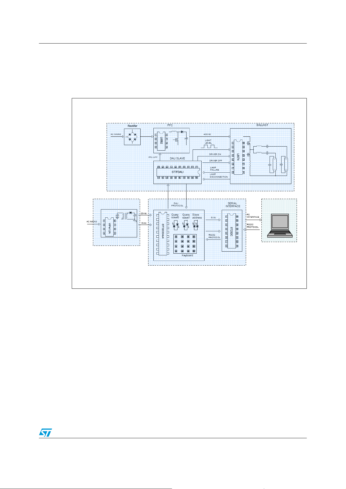
Figure 1 shows the block diagram of the system.
Figure 1. System block diagram
HIGH
FREQUENCY
BALLAST
ACíDC ADAPTER
SCI communication is considered as an option.
MASTER UNIT
SCI
Communication
Option
5/42
Page 6
Block diagram and system operating conditions AN2708
The present system has been designed according to the following specifications:
Table 1. System operating conditions
Parameter Value
Input voltage range 176-265 Vac/50 Hz; 90-140 Vac/60 Hz
Lamp type 2X36 W T8 tube lamps
Circuit power (max) 80 W
Lamp power (max) 72 W
Dimming range 5% to 100%
Power factor > 0.99
Current THD < 10%
Warm start < 1.5 sec
Standby mode power < 0. 6 W
In addition to the previous specs, the DALI communications are optically isolated, the digital
dimming is performed with high precision, and the lamp filament preheating time is
programmable as well as the ignition time.
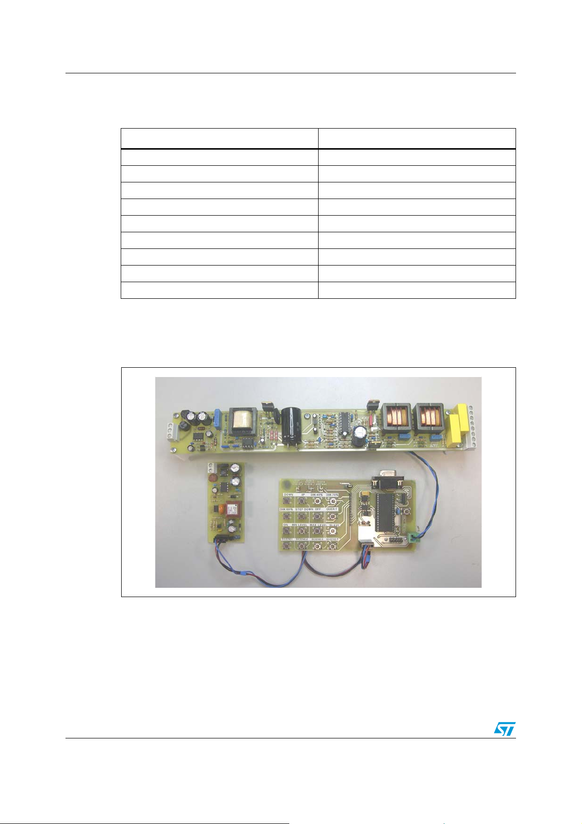
Figure 2. 2X36 W digital dimmable ballast with L6574 and ST7FDALI
HIGH FREQUENCY BALLAST
MASTER UNIT
MASTER UNIT
ACíDC
ACíDC
ADAPTE R
ADAPTE R
6/42
Page 7
AN2708 High-frequency ballast
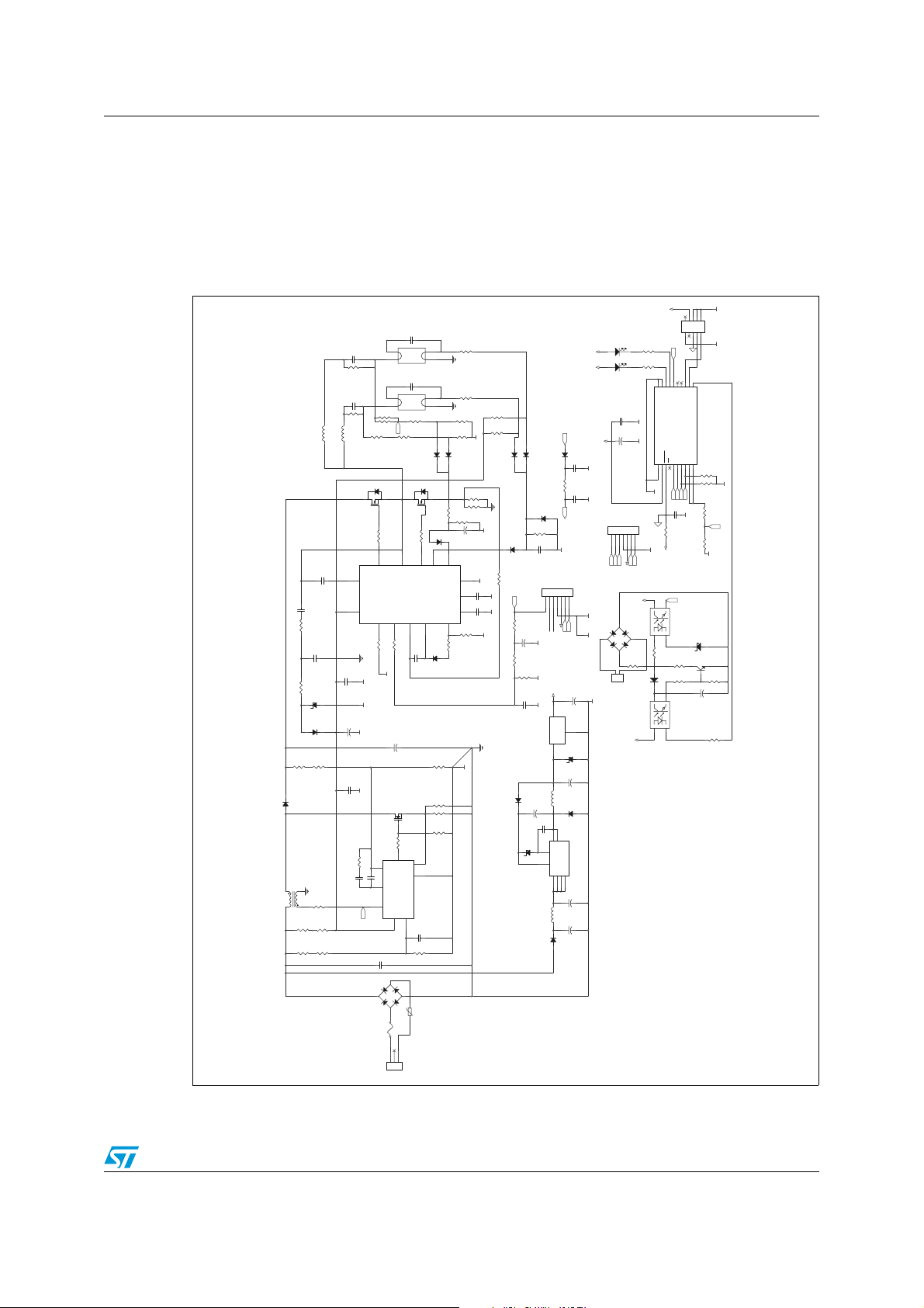
2 High-frequency ballast
This section describes the high-frequency ballast board which includes the power factor
correction stage, the half-bridge inverter driving circuitry, the output stage and the DALI
slave unit. The schematic of the board is shown in Figure 3.
Figure 3. Ballast schematic
5VDD
9
+1+3+5+7+
IC_GND
+2+4+6+8+
SIGN
IC_GND
IC_GND
0
R64
R63
CON7
IC_GND
5VDD
D17
2K49
1%
1%
2K49
19
20
OSC1/CLKIN
U11
VSS1VDD2RESET3SS/AIN0/PB04SCK/AIN1/ PB15MISO/AIN2/PB26MOSI/AIN3/PB37CLKIN/AIN4/PB48AIN5/PB59DALIIN/AIN6/PB6
IC_GND
Reset
R62
4
U10
112
R61
11K
BAS16
4
U9
112
J5
ICP Connector
10
Reset
PWM0
IC_GND
13
12
14
16
11
17
18
OSC2
PA0(HS)/LTIC
PA7/DALIOUT
PA1(HS)/ATIC
ST7FDALIF2M6
PA4(HS)/ATPWM2
PA3(HS)/ATPWM115PA2(HS)/ATPWM0
PA6/MC0/ICCCLK/BREAK
PA5(HS)/ATPWM3/ICCDATA
10
R70
1k 1%
R69
1k 1%
PB1
C45
100nF
4K7
1%
5VDD
334
SFH6156-2
2
1%
334
SFH6156-2
2
IC_GND
PB2
EN2
EN1
0
R68
50V
IC_GND
PIN3 SFH6156-2
R67
10K
1%
IC_GND
PIN3 SFH6156-2
D18
BZX284C 2V7
0.5W
Q4
BC817-25
312
R66
4R7
1%
R65
+
R72
3K16
1%
1%
332R
C46
22uF
20V
R71
1K21
1%
1600V
C20
8.2nF
C21
100nF
250V
1
23
Lamp2
T8 36W
1W
R30_2
100K
250V
C17
100nF
18
18
R30_1
100K
1W
L1
L2
1.8mH
1.8mH
213
Q2
16
C14
100nF
630V
C11
1nF
R17
22E 1W
Rs= max 5 ohm @100kHz
C10
4.7nF
R14
10E
DZ1
15V
On Air On Air
D3
1N4148
R9
750K
1%1%
D2
STTH1L 06
8 1
T1
5 4
TRANSFORMER
R6
R4
180K
R1
750KR2750K
VS
12
IC_GND
C19
100nF
0.5W
IC_GND
+
IC_GND
50V
C7
4.7uF
R10
750K
1%
IC_GND
C5
100n
R8
12K
C4
1000n
68K
PB2
R5
180K
1%
C1
R26_2A
R26_1
750K
STP8NM50
R21
10E
15
HVG
VBOOT
RPRE2OPIN+
R12
120K
1
C3
2
5
U1
100nF
BRIDGE
432
180K
R26_2
750K
R15
10K
IC_GND
23
R7
INV
330n
W08G
1
FUSE
4A/250V
Line
J1
1
23
SIGN
7
C6
+
33E
COMP
ZCD
VCC
8
C18
8.2nF
Lamp1
T8 36W
R27_2
750K
R27_1
750K
213
Q3
STP8NM50
R22
10E
14
OUT
U2
L6574
OPIN-6OPOUT5RING
C9
400V
47uF
Q1
STP8NM50
1
7
CS
GD
GND
U1
L6562
MULT
3
C2
R3
-+
NTC
15E@25° 3A
Neutral
123
CON3
4
1600V
4
LVG11EN18EN2
100nF
4
6
10nF
10K
1%
R29_2
15K
R29_1
15K
R24_2
680K
R28_2
4.7K
L1&L2: Choke Induc t or
- E25x13x7 core
- 2.62mm gap f or 1.8mH indu ct a nce
- 267 turns (AWG 40)
R24_1
680K
4.7K
R28_1
IC_GND
D5 BAT46
D7 BAT46
R23
330E
R20
D11
1N4148
EN1
EN2
9
GND
CPRE
CF
4
R1668K
D4
1N4148
R11
1%
9.53K
RS2
0.82E
1W
RS1
0.82E
1W
R13
47K
D6 BAT46
RS_2
1E
0.6W 0.6W
RS_1
1E
1K
+
IC_GND
C15
D8
1N4148
330uF 25V
IC_GND
10
R1910K
IC_GND
C13
PWM0
1000nF 25V
1
3
Rf
15K
C12
470pF
IC_GND
R18
68K
IC_GND
Rup
120K
C8
IC_GND
600V 1A
D14
STTH1L06
T1: Boost Inductor Spec (ITACOIL E2543/E)
- E25x13x7 core, 3C 85 f errite
- 1.5mm gap f or 0.7mH prim ar y inductanc e
- Primary: 105 turns (20 x 0.1mm)
- Secondary: 11 t ur ns (0 . 1m m )
SIGN
D61
BAT46
D9 BAT46
68K
1%
R100
D10
BAT46
PB1
R25
470E
IC_GND
C16
10nF 25V
J2
1234567
EN2
EN1
5VDD
PB2
+
Cf
Rlow
100nF
SIGN
50V
4.7uF
IC_GND
4.7K
5VDD
IC_GND
1
IC_GND
VOUT
GND
2
VIN
U7 LE50CZ
3
Cout
+
95mA
L3
1.8mH
CVdd
10uF 25V
+
2
Cfb
S1S
DZ2
15V 0.5W
22nF 25V
FB
3
Vdd
4
D5D6D7D
8
+
L4
680uH
240mA
+
D15
1N4007 1A 1000V
HSMG-C670
GREEN
LD2
5VDD5VDD
LD1
RED
HSMS-C670HE
C44
100nF
50V
C43
1uF
16V
+
5VDD
IC_GND
C72
33nF
50V
IC_GND
C73
50V
68pF
J4
1234567
PB2
EN1
EN2
5VDD
PWM0
CON7
3
-+
IC_GND
142
D16
MB2S
Vss_STDALI
C42
2.2uF16V
+
D12
18V 0.5W
10uF 25V
D13
STTH1L 06
600V
1A
U8 Viper12A
Cin2
3.3uF 450V
Cin1
3.3uF 450V
R60
1
2
J3
DALI Bus
CON2
Vss_ST7DALI
5VDD
7/42
Page 8
High-frequency ballast AN2708
This block is essentially a "double board" as the DALI slave board and its external circuitry
are mounted on a small separated board which is connected to the bottom side by means of
a 7-pin connector. Ta bl e 2 shows the ballast-slave communication.
Table 2. Ballast-slave communication
Pin ref. Description Analog stage Microcontroller
1 PWM0 (ref op-amp)
2 Disable L6574 EN1 & disconnected lamp
3 Enable L6574 EN2 & not ignited lamp
4GND
55 VDD
6 PB2 disable PFC
7 SIGN (lamp failure)
Table 3. Ballast bill of material
Reference Value Description
Bridge W08G 1.5 A 800 V Bridge rectifier
Cout, CVdd 10 µF 25 V Electrolytic cap
C7,Cf 4.7 µF 50 V Electrolytic cap
Cfb 22 nF 25 V Ceramic cap
Cin1,Cin2 3.3 µF 450 V Electrolytic cap
C1 100 nF 400 V Polyester cap
C2 10 nF 50 V Ceramic cap
C3 330 nF 50 V Ceramic cap
C4 1000 nF 50 V Ceramic cap
C5,C8,C9,C1
9
C6 47 µF 450 V Electrolytic cap
C14 100 nF 100 V Ceramic cap
C10 4.7 nF 100 V Ceramic cap
C11 1 nF 630 V Evox Rifa polypropylene cap Rs
C12 470 pF 50 V Ceramic cap
C13 1 µF 50 V Ceramic cap
C15 330 µF 25 V Electrolytic cap
100 nF 50 V Ceramic cap
= 5 Ω at 100 kHz
max
C16 10 nF 25 V Ceramic cap
C17, C21 100 nF 250 V Polyester cap
C18,C20 8.2 nF 1600 V Polyester cap
C42 2.2 µF16 V Electrolytic cap
8/42
Page 9

AN2708 High-frequency ballast
Table 3. Ballast bill of material (continued)
Reference Value Description
C43 1 µF 20 V SMD tantalum cap
C44,C45 100 nF 50 V 0805 SMD cap
C46 22 µF 20 V SMD tantalum cap
C72 33 nF 50 V 0805 SMD cap
C73 68 pF 50 V 0805 SMD cap
DZ1,DZ2 15 V 0.5 W Zener diode
D2,D13,D14 STTH1L06
D3,D4,D8,D1
1
1N4148 Small signal rectifier 200 mA 100 V
STMicroelectronics ultrafast high voltage rectifier 1 A 600
V
D5,D6,D7,D9
, D10,D61
D12 18 V 0.5 W Zener diode
D15 1N4007 1 A 1000 V General purpose rectifier
D16 MB2S 0.5 A 200 V SMD bridge rectifier
D17 BAS16 Small signal diode
D18 BZX284C 2V7 0.5 W Zener diode
FUSE 4 A 250 V Radial fuse
J1 Input 250 V connector 3-way PCB screw terminal, 5.08 mm
J2 Ballast-slave connector 7-way strip line socket
J3 Dali Bus 2-way vertical PCB header, 3.81 mm pitch
J4 Ballast-slave connector 7-way strip line connector
J5 ICP connector 10-way 2-row vertical through-hole boxed header
J13 4-way strip line socket
J14 4-way strip line connector
Lamp 1 Lamp connector 4-way PCB screw terminal, 5.08 mm
Lamp 2 Lamp connector 4-way PCB screw terminal, 5.08 mm
LD1 LS M67K-H2L1-1 2 mA red LED SMD 0805
LD2 LG M67K-G1J2-24 2 mA green LED SMD 0805
L1,L2 1.8 mH
L3 1.8 mH 95 mA Epcos BC series Axial inductor
L4 680 µH 240 mA Epcos LBC series Axial inductor
BAT46 DO 35 STMicroelectronics small signal Schottky diode
Choke inductor 2.62 mm gap, 267 turns (AWG40);
E25x13x7
NTC 15 Ω at 25 °C 3 A Inrush current suppressor
Q1,Q2,Q3 STP8NM50 TO220
STMicroelectronics N-CHANNEL 550 V 0.7 Ω - 8 A
MDmesh MOSFET
9/42
Page 10

High-frequency ballast AN2708
Table 3. Ballast bill of material (continued)
Reference Value Description
Q4 BC817-25 NPN small signal bipolar
RS_1,RS_2 1 Ω 0.6 W 1% metal film resistor
RS1,RS2 0.82 Ω 1 W resistor
R29_1,
R29_2,Rf
R28_1,
R28_2,Rlow
R12,Rup 120 kΩ Resistor
R1,R2,R9,
R10, R26_1,
R26_2,
R27_1,
R27_2
R15,R19 10 kΩ Resistor
R3 10 kΩ 0.6 W 1% resistor
15 kΩ Resistor
4.7 kΩ Resistor
750 kΩ 0.6 W 1% resistor
R4,R5,
R26_2A
R6,R16,R18 68 kΩ Resistor
R7 33 Ω Resistor
R8 12 kΩ Resistor
R11 9.53 kΩ 1% Resistor
R13 47 kΩ Resistor
R14,R21,R22 10 Ω Resistor
R17 22 Ω 1 W resistor
R20 1 kΩ Resistor
R23 330 Ω Resistor
R25 470 Ω Resistor
R60,R68 0 Ω SMD resistor 0805
R61 11 kΩ 1% SMD resistor 0805
R62 4.7 kΩ 1% SMD resistor 0805
R63,R64 1 kΩ 1% SMD resistor 0805
R65 330 Ω 1% SMD resistor 0805
R66 4.7 Ω 1% SMD resistor 0805
180 kΩ Resistor
R67 10 kΩ 1% SMD resistor 0805
R69,R70 1 kΩ 1% SMD resistor 0805
R71 1.2 kΩ 1% SMD resistor 0805
R72 3 kΩ 1% SMD resistor 0805
10/42
Page 11
AN2708 High-frequency ballast
Table 3. Ballast bill of material (continued)
Reference Value Description
R100 68 kΩ 1% SMD resistor 0805
R24_1,R24_
2
R30_1,R30_
2
T1 Transformer Choke boost inductor (ITACOIL E2543/E)
U1 L6562N STMicroelectronics transition-mode PFC controller
U2 L6574 STMicroelectronics ballast driver
U7 LE50CZ TO-92 STMicroelectronics very low drop voltage regulators
U8 VIPer12A-E DIP8
U9,U10 SFH6156-2 Optocoupler
U11 ST7FDALIF2M6 SO20
680 kΩ Resistor
100 kΩ 2 W resistor
STMicroelectronics offline SMPS primary IC 730 V 0.4 A
27R
STMicroelectronics
8-bit MCU with single voltage Flash memory, data
EEPROM, ADC, timers, SPI, DALI
Note: Resistors are 0.25 W unless specified. Q1, Q2 &Q3 are mounted with 8 °C/W heatsink.
2.1 PFC converter
This block allows drawing a quasi-sinusoidal current from the mains, in phase with the line
voltage in order to get a PF very close to 1 (more than 0.99).
To achieve such high PF the boost topology is implemented because of the advantages it
offers:
● Minimum number of external components, thus making it a low-cost solution
● Low input di/dt thus minimizing the noise generated at the input and, therefore, the
requirements on the input EMI filter
● The switch is source-grounded, therefore is easy to drive
However, boost topology requires the DC output voltage (400 Vdc) to be higher than the
maximum expected line peak voltage.
ST's L6562 has been used as the driver. It implements a transition mode control (fixed ON
time, variable frequency), that, for such output power, is preferred to the fixed frequency
average current mode being simpler and cheaper. The circuit operates on the boundary
between continuous and discontinuous current mode.
Besides providing good results in terms of power factor, this IC considerably reduces the
Total Harmonic Distortion (THD) as it reduces the conduction dead-angle that occurs to the
AC input current near the zero-crossings of the line voltage.
11/42
Page 12
High-frequency ballast AN2708
The basic design specifications are listed in Tab le 4 .
Table 4. PFC operating conditions
Parameter Value
Mains voltage range: Virms(min) - Virms(max) 90 – 265 Vac
Regulated DC output voltage: Vo 400 Vdc
Rated output power: Po 75 W
Minimum switching frequency: f
sw
Maximum output voltage ripple: ∆Vo < ± 10 V
35 kHz
Maximum overvoltage admitted: ∆V
Expected efficiency: η
PFC
OVP
60 V
> 90 V
For reference, it is useful to define also the following quantities:
● Input power: Pi (= Po / η ) ≈ 80 W
● Maximum mains RMS current: Iirms (= Pi/Virms(min)) ≈ 1 A
● Rated output current: Io (= Po/Vo) ≈ 0.2 A
The design guidelines are deeply explained in AN966 ("L6561, enhanced transition mode
power factor corrector"), AN1757 ("Switching from the L6561 to the L6562) and AN1089
("control loop model of L6561-based TM PFC"). The main design formulas are summarized
as follows inTab le 5.
Table 5. Power stage design equations
Input capacitor (C1) Boost inductor Power MOSFET (Q1) Boost diode (D1)
C1
Irms
------------------------------- ---------------------------------------- -=
2π fsw r Vinrmsmin⋅⋅⋅
where
r 0.01 0.1÷=
Output capacitor (C6)
Volume 4K L I2irms⋅⋅≥
V2irms Vo 2 Virms⋅–()⋅
L
-------------------------------- --------------------------------------------- -=
where
2fswPi Vo⋅⋅⋅
K1410
⋅⋅≅
V
Vo ∆V
DSS
2
Pon I
Qrms
where
3–
Ie
------------ -
Igap
I
Qrms
2 2 Iirms
OVP
⋅=
R
Vm inarg++=
DS on()
42
1
---------- -
---
9π
6
⋅–⋅⋅=
Virms
---------------- -
Vo
V
RRM
IF3Io⋅=
1.2 Vo⋅=
--------------------------------- ---------------- -
C6
≥
4π fVo∆Vo⋅⋅ ⋅
Po
Pcu
I2irms Rcu⋅⋅=
3
Pcross Vo Iirms t
⎛⎞
Pcap 3.3Coss V
⎝⎠
4
---
12/42
⋅⋅⋅=
fallfsw
1.5
drain
1
-- -
Cd V2drain⋅+⋅
2
P
lossesVTIDC
fsw⋅=
Rd I2rms⋅+⋅=
Page 13
AN2708 High-frequency ballast
Table 6. L6562 biasing circuitry design equations
Pin 1 (INV) Pin 2 (COMP) Pin 3 MULT Pin 4 (CS)
∆OVP R
V
out
high
R
-------------------------------- ---------- -
2.5
⋅=
6–
40 10
⋅⋅=
+()
highRlow
R
low
A RC-C network is
placed between this
pin and pin 1, leading
to a low crossover
frequency (some tens
of hertz) as well as to
an adequate phase
margin.
A small capacitor of 10 nF
filters the signal on MULT pin.
V
MULTpkx
------------------------------- -
Rlow
250 106–⋅
R
low
--------------------------------- -----
R
+
lowRhigh
-------------------------------- --------------- -=
2V
⋅
2.5
----------------------------- -==
250 106–⋅
2.5
inrmsmax
R
sense
Pin 5 (ZCD) Pin 6 (GND) Pin 7 (GD) Pin 8 Vcc
The supply voltage is
provided by a capacitive
power supply connected to
the half-bridge inverter.
R
start
Vout 2 V
m
--------------------------------- ---------------------------------------=
R6
≥
⋅–()
2.1 1.15⋅
Vout 2 V
---------------------------------- ------------------------------------ -
⋅–()
m310
⋅⋅
inrmsmax
inrmsmin
3–
IC ground. As a layout
hint, this pin has to be
kept separated from
power ground. All the
IC signals have to be
referred to this pin.
Gate driver.
A "bleeder" resistor between
the gate and the source is
used to avoid undesired
switch-on, without affecting
the power consumption.
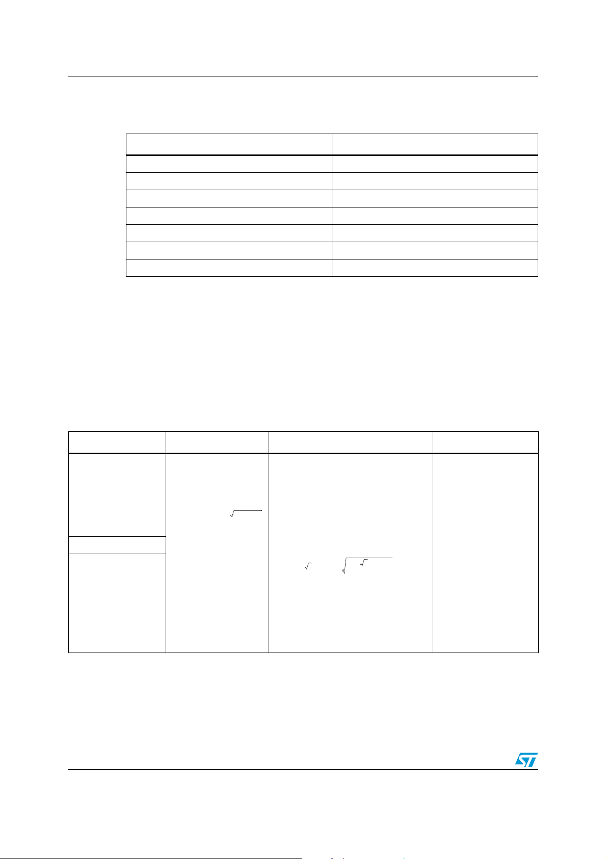
The PFC preregulator performances are shown in the following graphs:
Figure 4. PFC performances at 230 Vac-50 Hz
V
⎛⎞
inrmsmin
1.65 2.5
--------------------------------- --------------------------------------- -
≤
Pd Rs I
-------------------------------- -
⋅
⋅
⎜⎟
V
⎝⎠
inrmsmax
22I
⋅⋅
inrms
2
⋅=
Qrms
V
inrmsmin
-------------------------------- --------------=
I
2⋅
startup
CH1 (yellow): rectified input voltage
CH2 (blue): input current
13/42
Page 14

High-frequency ballast AN2708
2.2 Half-bridge inverter and ballast
A voltage fed series resonant half-bridge inverter has been implemented to drive the tubes.
This topology allows to easily operates in zero-voltage switching (ZVS) resonant mode,
heavily reducing the transistor switching losses and the electromagnetic interference. In
addition it guarantees design simplicity and low cost.
A parallel configuration has been chosen for the output stage. The half-bridge inverter
operating conditions and the ballast design have been obtained by assuming, for each lamp,
the following basic model:
Figure 5. Lamp ballast model
To increase the life time of the lamps a current mode preheat was preferred. The preheating
current brings the cathodes to the correct temperature, then a high voltage ignites the lamp
and finally the correct current guarantees the running power. These phases are ensured by
changing the frequency of the input voltage and properly selecting V
, L and C. During
IN
preheating and ignition, the lamp is not conducting and the circuit is reduced to a series L-C.
During running, the lamp is conducting and the circuit is an L in series with a parallel R-C. To
determine the optimum values for L and C and to calculate the ballast operating frequencies
the transfer functions for each mode of operation have to be inspected.
The table below shows the parameters and the values for a T8 36 W tube lamp which need
to be known in order to calculate the ballast operating conditions.
Table 7. Lamp parameters
Parameter Value
Input DC bus voltage: Vdc 400 V
Preheat current: Iph 0.6 A
Preheat time: Tph 1 sec
Max preheat voltage: Vphmax 300 Vpk
Ignition voltage: Vign 800 Vpk
Running lamp power: Prun 34 W
Running lamp voltage: Vrun 144 Vpk
Expected efficiency: η 95%
14/42
Page 15
AN2708 High-frequency ballast
Once the lamp and its parameters have been chosen, the ballast design will be optimized by
selecting the resonant components L and C as follows:
● Set Tpre
● Select frunmin (> 20 kHz)
● Choose ∆f = fmax-frunmin
● Select L & C such that fph > frun
● Select half-bridge switches
● Select L6574 biasing circuitry
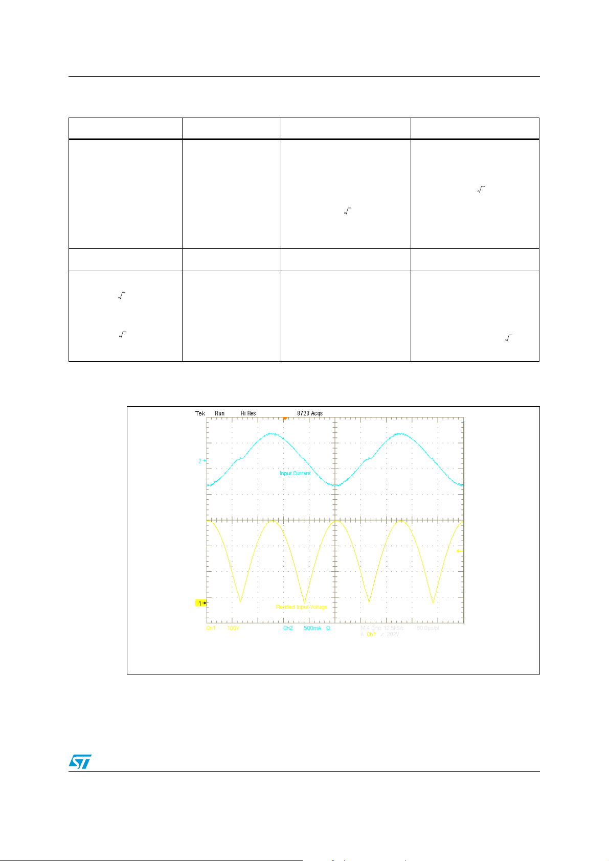
The magnitude of the transfer function (lamp voltage divided by input voltage) for the two
circuit configurations (preheating-ignition and running) illustrates the operating frequencies
and where they lie with respect to one another.
Figure 6. Ballast transfer functions (magnitude)
The currents and voltages corresponding to the resulting operating frequencies determine
the maximum current and voltage ratings for the inductor, capacitor, and the switches,
which, in turn, directly determine the size and cost of the ballast.
Moreover the zero-voltage switching is ensured as shown by the curves above in Figure 6.
STP8NM50 (8 A, 550 V) has been selected as power switch according to the current stress
and the input DC voltage.
The half-bridge inverter driving circuitry is based on the high performance L6574 which is an
OFF-LINE half-bridge driver designed in 600 V BCD technology, including all the features
needed to drive and properly control the tubes. A dedicated timing section in the L6574
allows setting the necessary parameters for proper preheat and ignition of the lamps. Also,
an op-amp is available to implement closed-loop control of the lamp current during normal
lamp burning. To avoid cross conduction of the power MOSFETs the internal logic ensures a
minimum deadtime. Moreover the L6574 is provided with two lamp status control functions
to protect the application against lamp failure as well as lamp disconnection. Finally it is
15/42
Page 16

High-frequency ballast AN2708
possible to modulate the output power in order to allow dimming by varying the switching
frequency.
The ballast operating frequencies determine the L6574 biasing circuitry as explained in
AN993 "Electronic Ballast With PFC Using L6574 and L6561" and as summarized below.
Table 8. L6574 biasing circuitry design equations for operating conditions
Pin 1 (CPRE) Pin 2 (RPRE) Pin 3 (CF) Pin 4 (RIGN) Pin 5 (OPOUT)
A capacitor is connected
Tph1.5 C
T
sh
K
PRE
---------------- -
10
⋅=
PRE
fph frun–
C
⋅=
PRE
----------------------- -=
R
1.41
PRE
Cf
1.41
frun
------------------- -= frun
RignCf
1.41
------------------- -=
RignCf
between this pin and OPINfor the current feedback loop
compensation. It set also the
turn on delay in a dimming
application.
2.2.1 Lamp dimming
In this system the lamps are dimmed down to 5% by interfacing the ST7FDALI
microcontroller with the analog driver L6574.
A PWM output of the ST7FDALI microcontroller is used to generate a 0-5 V PWM at 4 kHz.
Its integrated value gives the op amp voltage reference. The dimming level is set by varying
the PWM duty cycle from 70% (100% dimming) to 14% (5% dimming). This modification
allows changing the L6574 op-amp positive reference voltage from 120 mV to 20 mV which
increases the switching frequency and reduces the current in the load.
On the slave unit the duty cycle values have been calculated according the DALI protocol
brightness values, listed in Figure 7.
16/42
Page 17

AN2708 High-frequency ballast
Figure 7. DALI protocol brightness values
To avoid the presence of stationary waves along the tubes at minimum dimming level, a
resistor of 100 kΩ / 2 W has been placed in parallel to the battery capacitor of each lamp.
The resistance value ensures an additional current of 2 mA on the cathodes without
affecting the ballast efficiency.
Finally, during the startup sequence the frequency always goes from fmax to fmin,
independently of the set dimming level. Only after lamp turn-on does the frequency move
towards higher values.
2.2.2 Supply section
To supply the DALI slave microcontroller an AC-DC buck converter based on the
VIPer12A-E and L78L05 has been implemented on the ballast board. It converts the
rectified and filtered mains to a 5 V regulated output voltage dedicated to the
microcontroller. The converter works in discontinuous current mode adjusting the duty cycle
17/42
Page 18

High-frequency ballast AN2708
of the VIPer12A-E power switch in order to deliver the energy from the input to the output by
means of an inductor. PWM driver, power switch, thermal and overcurrent protection are
integrated in the same silicon chip ensuring minimum size and good performances at very
low cost.
Thanks to this implementation strategy the microcontroller is always supplied, allowing the
lamps to turn on, even when L6562 and L6574 are in a latched shutdown state.
The startup procedure is very important in an application that contains two different
sections. The ballast section starts before the PFC, avoiding any extra voltage at the PFC
section output, and consequently the L6562 OVP activation. This behavior is guaranteed
under all conditions because the VS turn-on threshold of L6574 is lower than that of the
L6562. The turn-on threshold is reached by a resistor chosen in order to ensure the startup
current of both the L6562 and the L6574. When the ballast section is running, the charge
pump (C11, R14, D3 and DZ1) supplies both the devices and the filter R17-C10 allows to
reduce the noise at Vcc.
2.2.3 Lamp turn-on and lamp turn-off
To get low-power consumption (less than 0.6 W) during the lamps’ turnoff state, both the
half-bridge and the PFC have to be disabled, even in the presence of the mains at the
ballast input. To manage this standby condition the L6574 control section and the L6562
ZCD pin are interfaced with the DALI slave microcontroller.
Short pulses (> 200 nsec) at the EN1 and EN2 inputs are recognized by the L6574. In
particular, EN1 high (> 0.6 V) stops all the half-bridge functions and puts the L6574 in a
latched shutdown state. At the same time, by forcing externally the ZCD pin to a voltage
below 150 mV, the L6562 is stopped. To cancel this status, in order to turn on the lamps, a
pulse (>0.6 V) is sent by the microcontroller to the L6574 second control pin EN2 and the
ZCD pin external pull down is removed. The half-bridge driver restarts the preheating and
ignition procedure, and the L6562 performs again its operation. The controls timing diagram
is shown in Figure 8.
18/42
Page 19
AN2708 High-frequency ballast
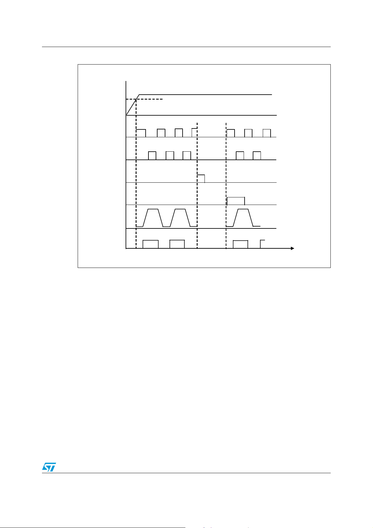
Figure 8. Ballast controls timing chart
Vsupply
LVG
HVG
Latched
Disable
EN1
Forced
Restart
EN2
ZCD
GD
TIME
On the slave unit the turning ON/OFF process is implemented by setting the pins PB3 (EN1)
and PB4 (EN2) as output pull-up, while PB2 (ZCD) as output open drain. The three
corresponding bits in the port data register are clear by software. To "switch on" the ballast,
a pulse must be sent to PB4 (EN2 signal) and the third bit must be set in the port B (ZCD)
data register. To "switch off" the ballast, a pulse must be sent to PB3 (EN1 signal) and the
third bit must be cleared in the port B (ZCD signal) data register.
Figure 9, 10, and 11 show the idle state and the turn-on/off commands.
19/42
Page 20

High-frequency ballast AN2708
Figure 9. Idle state
CH3 (blue): EN1 low level
CH4 (green): EN2 low level
Figure 10. Turn-on procedure
CH3 (blue): EN1 low level
CH4 (green): EN2 pulse
Figure 11. Turn-off procedure
CH3 (blue): EN1 pulse
CH4 (green): EN2 low level
20/42
Page 21

AN2708 High-frequency ballast
2.2.4 Verification of lamp status
This function detects a lamp disconnection or a lamp failure on the slave board. The
microcontroller performs a double check: one on the PB1 pin for the lamp hardware status
and one on the flag "LAMP_ARC_POWER_ON" for the lamp software status. If the PB1
logical level is low and the flag is true, lamp disconnection happened. The condition is
recorded on ST7FDALI, so when the microcontroller receives a "query frame" from the
master, it changes the PB3 (EN1) and PB4 (EN2) configuration from input to output, and
sends a byte answer as 'STATUS INFORMATION' described below:
● bit 0 status of ballast; '1'= NOK
● bit 1 Lamp failure; '1'= NOK
● bit 2 Lamp arc power on; '0' = OFF
● bit 3 Query: Limit Error; '0' = Last requested arc power level is between MIN..MAX
LEVEL or OFF
● bit 4 Fade ready; '0' = fade is ready; '1' = fade is running
● bit 5 Query: 'RESET STATE'? '0' = 'No'
● bit 6 Query: Missing short address? '0' = 'No'
● bit 7 Query: 'POWER FAILURE'? '0' = 'No'; 'RESET' or an arc power control command
has been received after last power-on
When the master receives this frame, it displays the lamp status by means of two LEDs
(green stands for ok, red for status not ok). Once the failure condition has been detected
and solved, an "ON" command has to be sent to the slave, allowing the master's
microcontroller to toggle again the LED status from red to green. From the analog side, to
detect a disconnection or a failure event for each lamp, two signal Schottky diodes have
been used to bias the EN1 or EN2 pin of L6574. The failure condition is detected both at
startup and when running.
The forward and backward frame timing is shown in Figure 12 and 13:
Figure 12. Forward frame timing
21/42
Page 22

High-frequency ballast AN2708
Figure 13. Backward frame timing
The forward as well as the backward frame duration is the same for all kinds of commands.
2.2.5 Ballast performances
In this section the main ballast waveforms are shown.
Figure 14. Ballast startup at 230 Vac-full
power
CH2 (blue): lamp current
CH3 (magenta): V
CPRE
CH4 (green): supply voltage
Figure 15. Lamps turn-on at 230 Vac-full
power
CH1 (yellow): lamp1 voltage
CH2 (blue): lamp1 current
CH3 (magenta): lamp2 voltage
CH4 (green): lamp2 current
22/42
Page 23
AN2708 High-frequency ballast
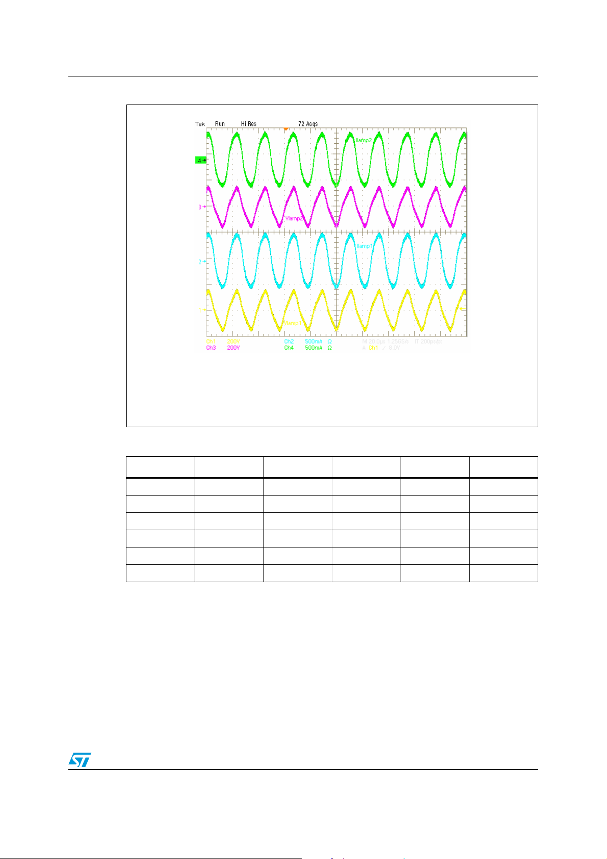
Figure 16. Lamps running at 230 Vac - full power
CH1 (yellow): lamp1 voltage
CH2 (blue): lamp1 current
Ch3 (magenta): lamp2 voltage
CH4 (green): lamp2 current
Table 9. Ballast performances
Vin (Vac) Pin (W) PF THD (%) Po (W) η (%)
90 76.5 0.999 3.9 66 86.2
110 75.5 0.999 3.6 66 87.4
140 74.2 0.998 5.5 66 89
176 73.7 0.997 7.2 66 90
230 73 0.997 7.3 66 90
265 72.8 0.996 8.3 66 91
The efficiency of the system is a little bit lower than a standard HF ballast due to the supply
section of the slave and the resistors in series to the lamp’s cathode used to ensure a
minimum current at low dimming level.
23/42
Page 24

DALI master unit AN2708
3 DALI master unit
The ST2C334J4 microcontroller is used as master, implementing the DALI Peripheral via
software.
The communication master-slave uses a 20 V bus. To adapt the TTL level of the
microcontroller to the communication bus level, two opto-couplers and a NPN transistor BC817 have been used.
The RS232 interface with ST232C is available on the board to implement the SCI
communication as an option. This option expects the use of a PC to address the ballast
either with broadcast or group or single mode thanks to a GUI called (DALI Power Control).
The DALI master unit has been thought of as a standalone solution. In fact it is provided
with a keyboard to manage the DALI commands, to address the slaves and to display the
lamps’ status.
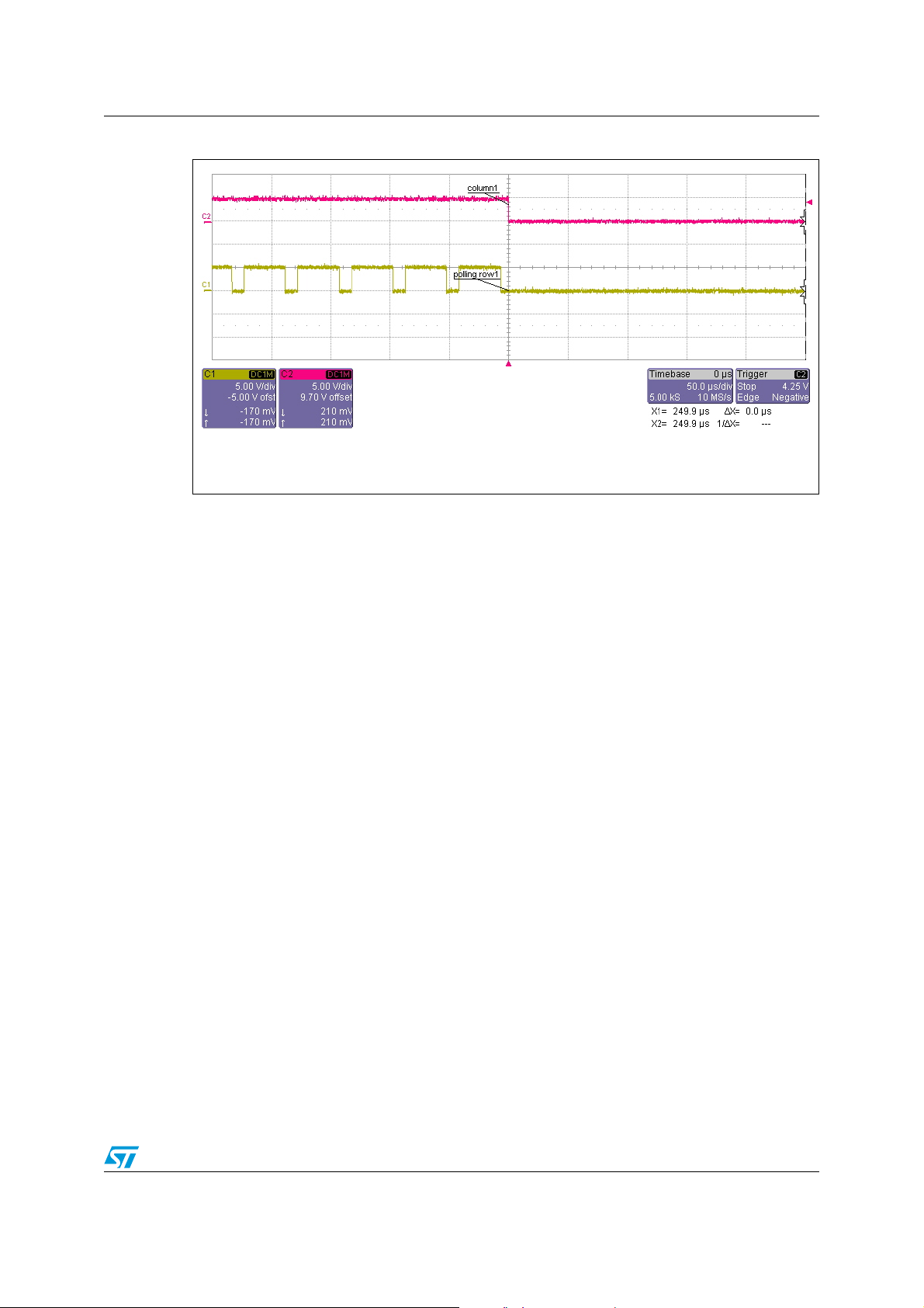
The keyboard is made up of 16 push buttons controlled by means of a matrix
representation. In particular the first four pins of PORTD are associated to the rows and the
first four pins of PORTB to the columns.
The check of the keyboard is implemented as a loop mode by clearing the PDDR register
port and setting the PBDR register port sequentially. When a button is pressed, the pin of
the port B corresponding to the interested column goes down and this condition is taken
over by an interrupt condition. Inside the interrupt routine, a read procedure of the port
registers PDDR and PBDR is expected and by this information the pressed button is
acknowledged. The “press button” procedure is described by Figure 17 and 18.
Figure 17. Polling keyboard
CH1 (yellow): row polling
CH2 (purple): column level
24/42
Page 25
AN2708 DALI master unit
Figure 18. Pressed button event
CH1 (yellow): row polling
CH2 (purple): column level
25/42
Page 26
DALI master unit AN2708
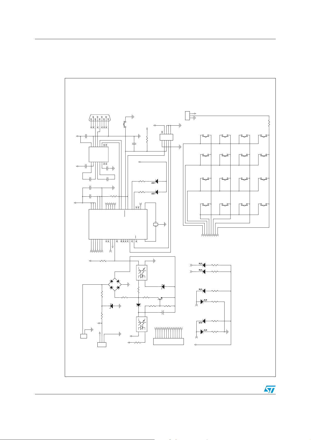
3.1 Master unit schematic and bill of material
The schematic of the master unit is shown in Figure 19.
Figure 19. Master unit schematic
5VDD
3
2
P1
C48
100nF
50V
5VDD
16
15
14
VDD
GND
T1OU T
C1+1V+2C1-3C2-5V-6T2OU T7R2IN8C2+
U13
5VDD
C47
50V
100nF
C51
100nF
50V
C50
50V
100nF
C49
220nF
50V
5VDD
8
36
VDDA
VDD_125VDD_2
U12
AIN0/PD02AIN1/PD13AIN2/PD24AIN3/PD35AIN4/PD46AIN5/PD57MCO/ PF 010BEEP/PF111PF212OCMP1_A/PF413ICAP1_A/(HS)/PF614EXTCLK_A/(HS)/PF715OCMP2_B/PC016OCMP1_B/PC117ICAP2_B/(HS)/PC218ICAP1_B/(HS)/PC319ISPDATA/MISO/PC420MOSI/PC521SCK/ISPCLK/ PC622SS'/PC723OSC1
RS232
594837261
SW1
Reset
13
11
9
12
T2IN10T1IN
R1IN
R2OUT
R1OUT
ST232C
4
C53
100nF
50V
C52
100nF
50V
R76
Col4
Col3
Col2
Col1
9
VSSA
PB4
1
PB039PB140PB241PB342PB4
33
VSS_126VSS_2
C54
10K
1%
30
37
38
31
32
RESET
ISPSEL
PE0/TD0
PE1/RD1
100nF
5VDD
PA4(HS)27PA5(HS)28PA6(HS)29PA7(HS)
5VDD
5VDD
9
+1+3+5+7+
+2+4+6+8+
J8
4.7K
R82
50V
R81
1K
R80
1K
PA3
34
24
PA3
OSC2
35
10
LD4
LG M67K-G1J2-24
Green
LD3
Red
LS M67K-H2L1-1
16MHz
Y1
ST72C334J4B6
1
J18
Pull-Up Jumper
R102
SW23SW24 SW25
ICP Connector
Porta
PD3
Row4
SW20 SW21
Porta
PD2
Row3
SW19
Porta
PD1
Row2
Porta
PB0
Colomn4
Porta
PB1
SW18
Porta
PD0
Row1
Rows
Row2
Row4
Row3
SW22
Columns
Row1
Col2
Col1
Col4
Col3
SW27SW28
SW30
Colomn3
Porta
PB2
SW26
SW31 SW32 SW33
Porta
PB3
Colomn2
Colomn1
SW29
10k
Row1
Row2
Row3
5VDD
R74
R7305%
VD
1
2
J6
DALI Bus
J7
TRANSM.
Row4
AIN5
PF2
R75
10K
1%
3
-+
1
D20
MB2S
4
5% 1W
220R
D19
BZX85C22
5VDD AIN4
123
Supply Volt age
4
334
SFH6156-2
U15
112
2
R77
0
TRAN SM.
2
R79
11K
1%
R84
4R7
1%
D21
BAS16
R83
4
334
SFH6156-2
U14
112
2
5VDD
J9
R78
1K2
1%
26/42
321
1%
330R
PA3
D28
LG M67K-G1J2-24
R91
1K
Query status
Query status
5VDD
Green
R90
1K
D27
Green
LG M67K-G1J2-24
R89
Green
D26
LG M67K-G1J2-24
1K
R88
1K
D25
PA3
Red
LS M67K-H2L1-1
R87
1K
Green
LG M67K-G1J2-24
D24
R86
1K
Red
D23
PB4
LS M67K-H2L1-1
AIN5
Slave address
AIN4
D22
BZ84C 2V7
Q5
BC817-25
3K
1%
R85
+
C55
22uF
25V
Row2
Row1
Row4
Row3
AIN4
PF2
AIN5
Col2
Col4
Col3
Col1
PB4
12345678910111213
Page 27

AN2708 DALI master unit
Table 10. Master unit bill of material
Reference Value Description
C47,C48,C50,C51,C52,
C53,C54
C49 220 nF 50 V Ceramic capacitor SMD 0805
C55 22 µF 25 V Tantalum capacitor SMD
D19 BZX85C22 22 V 0.5 W Zener diode
D20 MB2S SMD bridge rectifier
D21 BAS16 SMD diode
D22 BZ84C 2V7 2.7 V 0.5 W Zener SMD diode
D23,D25 LS M67K-H2L1-1 Red SMD LED 2 mA, 0805
D24,D26,D27,D28 LG M67K-G1J2-24 Green SMD LED 2 mA, 0805
J6 DALI BUS 2-way single row, header shrouded
J7 Supply voltage 3-way single row header shrouded
J8 ICP connector
J9 13-way strip line connector (not mounted)
J12 Pull-up jumper 3-way strip line connector
LD3 LS M67K-H2L1-1 Red SMD LED 2 mA, 0805
LD4 LG M67K-G1J2-24 Green SMD LED 2 mA, 0805
100 nF 50 V Ceramic capacitor SMD 0805
10-way 2-row vertical through-hole boxed header, 2.54 mm
pitch/grid
P1 Serial connector 9-way 90° PCB mount D plug
Q5 BC817-25 SMD NPN transistor
R73 0 Resistor SMD 1206
R77 0 Resistor SMD 0805
R74 220 Ω 1 W 5% resistor
R75,R76 10 kΩ 1% resistor SMD 0805
R78 1.2 kΩ 1% resistor SMD 0805
R79 11 kΩ 1% resistor SMD 0805
R80,R81 1 kΩ Resistor SMD 0805
R82 4.7 kΩ Resistor SMD 0805
R83 330 Ω 1% Resistor SMD 0805
R84 4.7 Ω 1% Resistor SMD 0805
R85 3 kΩ 1% Resistor SMD 0805
R86,R87,R88,R89,R90,
R91
R101 10 kΩ Resistor SMD 0805
SW1 Reset THT button
1 kΩ Resistor SMD 0805
27/42
Page 28

DALI master unit AN2708
Table 10. Master unit bill of material (continued)
Reference Value Description
SW2, SW3, SW4, SW5,
SW6, SW7, SW8, SW9,
SW10, SW11, SW12,
SW13, SW14, SW15,
SW16, SW17
U12
U13 ST232C SOP
U14,U15 SFH6156-2 SMD Opto-coupler
Y1 16 MHz Oscillator
Keyboard THT button
ST72C334J4B6
PSDIP42
8-bit MCU with single voltage flash memory, Adc, 16-bit timers,
STMicroelectronics 5 V powered multi-channel
STMicroelectronics
SPI, SCI interface
RS-232 drivers and receivers
Note: Resistors are 0.25 W unless specified
28/42
Page 29
AN2708 Basics of DALI
4 Basics of DALI
DALI stands for "Digital Addressable Lighting Interface". It is a standard interface for lighting
control solutions, defined by the main lighting manufacturers and standardized as IEC 929.
The DALI protocol is implemented on a master-slave architecture.
It uses the bi-phase Manchester asynchronous serial data format. All the bits of the frame
are bi-phase encoded except the two stop bits. Following are some of the standard features:
● Transmission rate at 1.2 kHz.
● Bi-phase bit period is 833.33 µS ±10%.
A forward frame consists of 19 bi-phase encoded bits:
– 1 start bit (0->1: logical '1')
– 1 address byte (8-bit address)
– 1 data byte (8-bit data)
– 2 high level stop bits (no change of phase)
A backward frame consists of 11 bi-phase encoded bits:
– 1 start bit (0->1: logical '1')
– 1 data byte (8-bit data)
– 2 high level stop bits (no change of phase)
Each frame has 2 stop bits which do not contain any change of phase.
The setting time between two subsequent forward frames is 9.17 ms (minimum), while the
delay between forward and backward frame goes from 2.92 ms to 9.17 ms. If a backward
frame has not been started after 9.17 ms, this is interpreted as "no answer".
In the event of code violation, the frame is ignored and the system is ready again for data
reception.
The main advantages of the DALI system can be summarized as follows:
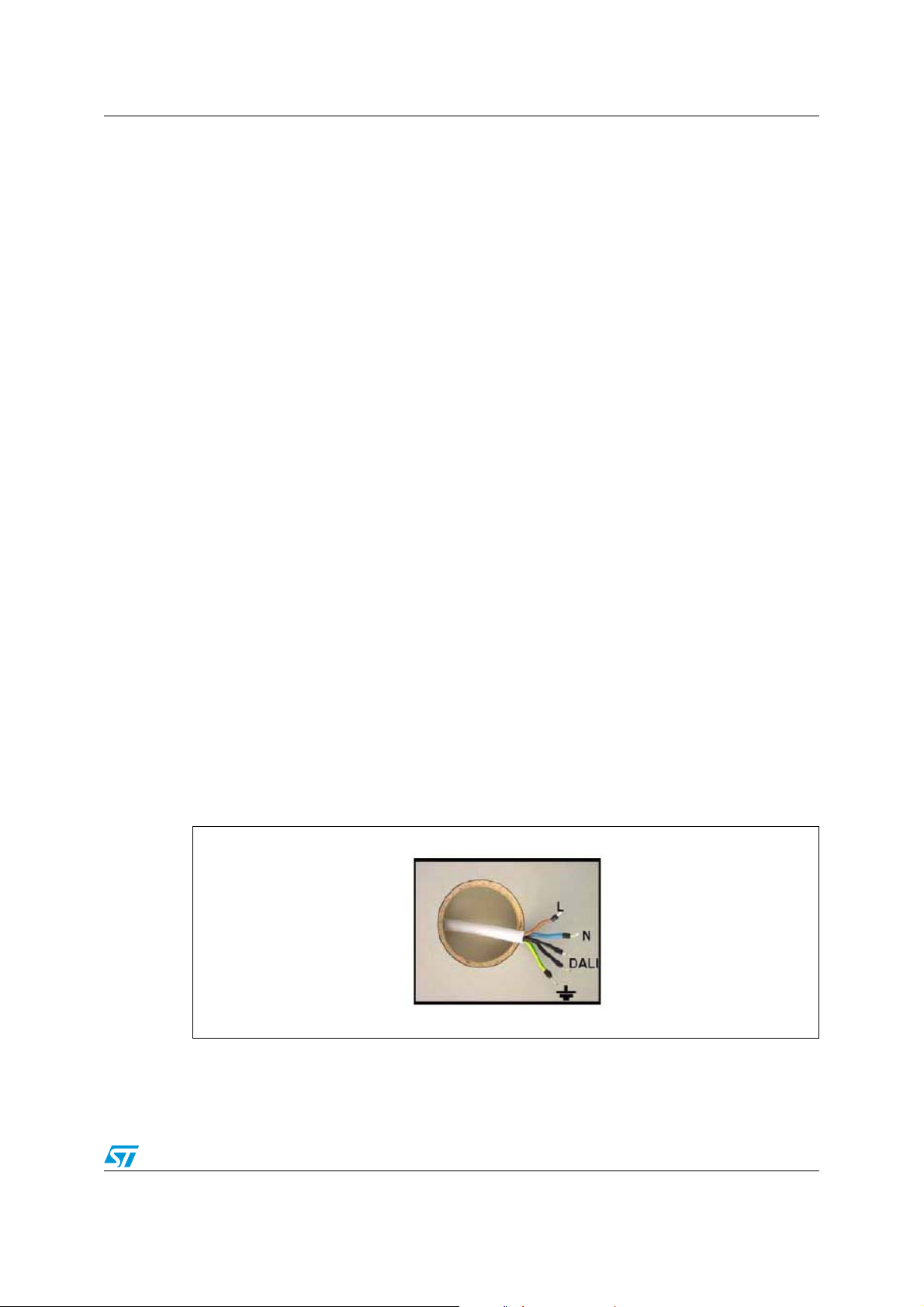
● Simple wiring: all of the units in the system are interconnected using a simple five-core
cable.
Figure 20. Cable wiring
29/42
Page 30
Basics of DALI AN2708
N
N
N
N
● No mains switching required: lamps can be dimmed or switched on and off using
control system commands without any need for mains switching.
● Easy system re-configuration: the configuration of the system can be changed quickly
without any modification to the hardware.
● Easy system modification: if the lighting system needs to be enlarged, new
components can be added anywhere on the DALI cable.
● It is possible to define light scenes. A scene means a particular light level intensity. 16
scenes can be defined at maximum.
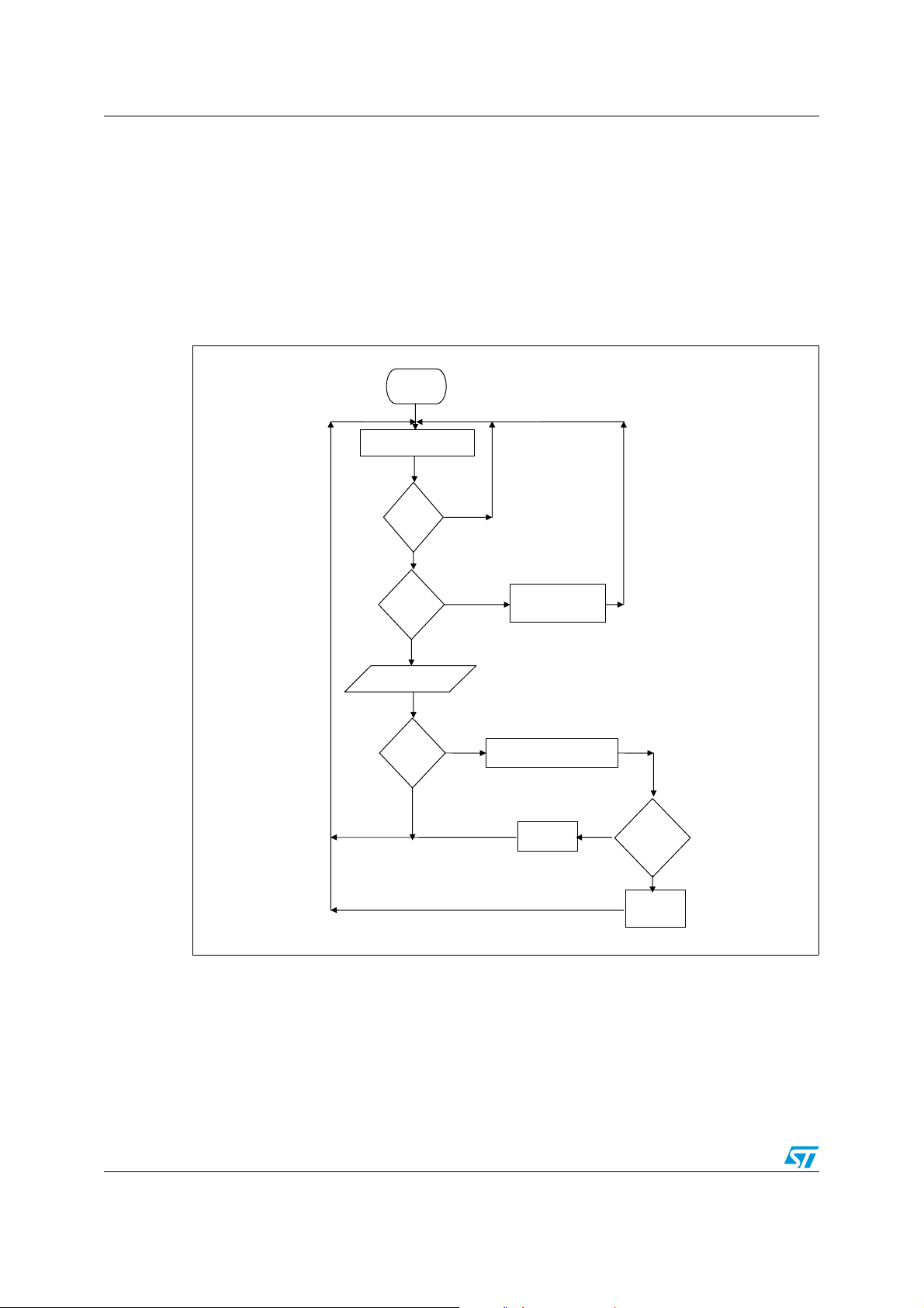
Figure 21. Master flowchart
START
POLLING KEYBOARD
PUSH
BUTTON
Y
BUTTON
NUMBER
11
SEND COMMAND
QUERY
FRAME
Y
Y
CHANGE SLAVE
ADDRESS
WAIT BACKWARD FRAME
NO
ANSWER
FRAME
RECEIVED
Y
TOGGLE
LED
30/42
Page 31

AN2708 Basics of DALI
g
,
d
Figure 22. Slave flowchart
Start
Main
New Frame Received
PWM
routine
Failure=1
Dali Peripheral
Pulse on EN1(OFF) or
EN2 (ON) change pin
confi
uration
Y
Pin
PB1=low
level
N
Process
Command
ON/
Y
OFF
N
Y
Other indirect
arc power control
comman
s
N
Query
N
command
Y
Send Lamp
OK
N
Failure=1
Y
Change
configuration
of PB3
PB4pin
Send Lamp
Failure
31/42
Page 32

DALI master AC-DC adapter AN2708
5 DALI master AC-DC adapter
This is an offline wide-range double-output SMPS based on the VIPer12A-E. The first
output, 20 V at 100 mA, is dedicated to the bus communication allowing to address up to 64
slaves, while the second one delivers 5 V at 10 mA to the MASTER DALI microcontroller
thanks to a linear post-regulator.
The VIPer12A-E combines on the same silicon chip a dedicated current mode PWM
controller, a high voltage power MOSFET and the protection features (thermal, overcurrent,
and overvoltage) which increases the converter reliability and saves size, parts count and
cost.
The converter topology is an isolated flyback designed to work in discontinuous current
mode according to the following specifications:
Table 11. SMPS operating conditions
Parameter Value
Input voltage range 90 – 265 Vac
Input frequency range 50/60 Hz
Output voltage 1 V1=20 V
Output voltage 2 V2=5 V
Output current 1 I1=100 mA
Output current 2 I2=10 mA
Output power (peak) 2.2 W
Line regulation +/- 1%
Load regulation +/- 1%
EMI EN55015
5.1 Adapter description
The schematic of the board is shown in Figure 23.
The AC input is rectified by the diodes bridge and then filtered by the bulk capacitor C1, and
C2 to generate the high voltage DC.
The input EMI filter is a simple CLC PI filter for both differential and common mode noise
suppression.
An NTC limits the inrush current and ensures a reliable operation of the bridge at startup.
The switching frequency is fixed at 60 kHz by the IC internal oscillator allowing optimization
of the transformer size and cost. An RCD snubber circuit (R92, C59, D30) reduces the
leakage inductance voltage spike and the voltage ringing on the drain pin of VIPer12A-E.
As soon as the voltage is applied on the input of the converter the high voltage startup
current source connected to the drain pin is activated and starts to charge the Vdd capacitor
C8 by a constant current of 1mA. When the voltage across this capacitor reaches the Vddon
threshold (about 14 V) the VIPer12AS-E starts to switch. During normal operation the smart
32/42
Page 33

AN2708 DALI master AC-DC adapter
power IC is powered by the auxiliary winding of the transformer via the diode D31. No spike
killer for the auxiliary voltage fluctuations is needed thanks to the wide range of the Vdd pin
(9-38 V). The primary current is measured using the integrated current sensing for current
mode operation.
The output rectifier D29 has been chosen in accordance with the maximum reverse voltage
and power dissipation. In particular a 1 A - 150 V power Schottky, type STPS1150, has
been selected.
The output voltage regulation is performed by secondary feedback on the 20 V output while
the 5 V output, is linearly post-regulated from the 20 V output. This operation is performed
by a low drop voltage regulator, L78L05CZ, in the TO92 package. The feedback network
consists of a programmable voltage reference, TL431, driving an optocoupler which ensures
the required insulation between the primary and secondary sections. The optotransistor
drives directly the VIPer12A-E feedback pin which controls the operation of the IC.
A small LC filter has been added on the 20 V output in order to reduce the high frequency
ripple with reasonable output capacitor value.
The flyback transformer is a layer type based on the EF13 core and Fi 324 ferrite,
manufactured by Vogt, and ensures safety insulation in accordance with the EN60950.
Figure 26 shows the main features of the transformer. The power supply has been
implemented on a double-sided 35 µm PCB in FR-4, sizing 81 x 37 mm.
Figure 23. Adapter schematic
L9
3
C61
2.2nF Y 1
+
1mH 130m A
C56
+
2.2uF
4
Vdd
FB
3
U18
VIPer12A
BRIDGE2
4
DF06
NTC2
10R @ 25°
J17
2
Input 250V Con
1
FUSE2 0.5A
T1: S MT
- EF12.6/3. 7c ore, F i324 f errite
- 0.16mm gap f or 2m H prim ary induc t anc e
- Primary : 135 t urns (0. 14m m -AW G35)
- Secondary: 28 turns (0.36mm-AWG27)
- Auxiliary : 21 t urns (0. 05m m -AW G44)
1
-+
2
C63
10uF
50V
5
+
2
C57
2.2uF
400V400V
STTH1L06
U17
PC817
43
R93
560R
C6510nF
+
L8
100uH 600mA
C59
150uF
35V
12
U19
2 1
TL431
20V@100mA
C60
+
22uF
35V
U16
L78L05CZ
VIN3VOUT
R96
R95
33K
1K
R98
150K
C64
100nF
50V
3
R99
4.7K
1
GND
2
2.2uF
5V@10mA
C62
+
Supply Volt age
J10
1
2
3
R92
C58
56K
D30
R94
10R
D31
1N4148
8
D
D7D6D
S1S
470pF
1kV
1
2
4
5
SL 060 918 11 01
D29
STPS1150
T3
9
6
R97
10K
50V
33/42
Page 34

DALI master AC-DC adapter AN2708
Figure 24. Adapter PCB layout - top side -
silkscreen (to scale)
Figure 26. Flyback transformer
Figure 25. Adapter PCB layout - bottom side -
copper tracks (to scale)
● Operating switching frequency: 60 kHz
● Core geometry: EF 12.6/3.7
● Core material: FI 324 or equivalent
● Primary inductance value: 2 mH
● Leakage inductance: 75 µH
● Air gap length: 0.16 mm
● Safety: EN60950
34/42
Page 35

AN2708 DALI master AC-DC adapter
5.2 Adapter bill of material
Table 12. Adapter bill of material
Reference Value Description
BRIDGE2 DF06M 1 A 600 V Bridge rectifier
C56,C57 2.2 µF 400 V Electrolytic cap
C58 470 pF 1 kV Ceramic cap
C59 150 µF 35 V Low ESR electrolytic cap
C60 22 µF 35 V Low ESR electrolytic cap
C61 2.2 nF Y1 Y1 ceramic cap
C62 2.2 µF 25 V Electrolytic cap
C63 10 µF 50 V Electrolytic cap
C64 100 nF 50 V Ceramic cap
C65 10 nF 50 V Ceramic cap
D29 STPS1150 STMicroelectronics power Schottky rectifier 1 A 150 V
D30 STTH1L06 STMicroelectronics ultrafast high-voltage rectfifier 1 A 600 V
D31 1N4148 Small signal rectifier 200 mA 100 V
FUSE2 0.5 A Radial fuse
J10 Supply voltage 3-way single row shrouded header
J11 Input 250 V connector 2-way PCB screw terminal, 5.08 mm
L8 100 µH 600 mA Axial inductor
L9 1 mH 130 mA Axial inductor
NTC2 10 Ω @ 25° Inrush current suppressor
R92 56 kΩ Resistor, metal film 0.25 W
R93 560 Ω Resistor, metal film 0.25W
R94 10 Ω Resistor, metal film 0.25 W
R95 1 kΩ Resistor, metal film 0.25 W
R96 33 kΩ Resistor, metal film 0.25 W
R97 10 kΩ Resistor, metal film 0.25 W
R98 150 kΩ Resistor, metal film 0.25 W
R99 4.7 kΩ Resistor, metal film 0.25 W
T3 SL 060 918 11 01 VOGT SMT
U16 L78L05CZ TO92 STMicroelectronics positive voltage regulator
U17 PC817 Sharp Optocoupler 5 kV
U18 VIPer12A-E DIP8 STMicroelectronics offline SMPS primary IC 730 V 0.4 A 27 Ω
U19 TL431 TO92 STMicroelectronics programmable voltage reference
35/42
Page 36

DALI master AC-DC adapter AN2708
5.3 Adapter performances
Several tests have been performed on the board to evaluate the converter behavior in terms
of efficiency, stability, safe operating area of the devices, line & load regulation and EMI
performances.
5.3.1 Steady state tests
These tests have been performed at the input voltage of 110 Vac and 230 Vac at full and
minimum load condition.
Figure 27. VIPer12A-E steady state behavior at
f u l l l o a d a t 1 1 0 V a c - 6 0 H z
CH1 (blue): drain voltage
CH4 (purple): drain current
As shown by the waveforms the power supply operates in discontinuous current mode.
Figure 29. VIPer12A-E steady state behavior at
minimum load at 110 Vac - 60 Hz
Figure 28. VIPer12A-E steady state behavior at
full load at 230 Vac - 50 Hz
CH1 (blue): drain voltage
CH4 (purple): drain current
Figure 30. VIPer12A-E steady state behavior at
minimum load at 230 Vac - 50 Hz
CH1 (blue): drain voltage
CH4 (purple): drain current
36/42
CH1 (blue): drain voltage
CH4 (purple): drain current
Page 37

AN2708 DALI master AC-DC adapter
At minimum load the VIPer12A-E ensures the burst mode operation, saving the input power
consumption.
5.3.2 Startup behavior
Figure 31, 32, 33, and 34 show the typical waveforms during the startup of the power supply.
In particular, the full load condition is considered since it represents the heaviest case in
terms of voltage and current stress, as well as the minimum load condition for loop stability
and voltage stress.
Figure 31. Startup waveforms at full load
at 110 Vac - 60 Hz
CH1 (blue): drain voltage
CH2 (red): 5 Vout
CH3 (green): 20 Vout
CH4 (purple): drain current
Figure 32. Startup waveforms at full load
at 230 Vac - 50 Hz
CH1 (blue): drain voltage
CH2 (red): 5 Vout
CH3 (green): 20 Vout
CH4 (purple): drain current
37/42
Page 38

DALI master AC-DC adapter AN2708
Figure 33. Startup waveforms at minimum
load at 110 Vac - 60 Hz
CH1 (blue): drain voltage
CH2 (red): 5 Vout
CH3 (green): 20 Vout
CH4 (purple): drain current
There is no overshoot on the output voltages and the measured wakeup time is 180 mS.
5.3.3 Dynamic load tests
Figure 34. Startup waveforms at minimum
load at 230 Vac - 50 Hz
CH1 (blue): drain voltage
CH2 (red): 5 Vout
CH3 (green): 20 Vout
CH4 (purple): drain current
These tests show the transient load response at 110 Vac and 230 Vac mains when the 20 V
output current is increased from 10% to 90% of the maximum value.
Figure 35. Dynamic load waveforms
at 110 Vac - 60 Hz
CH3 (green): 20 Vout voltage ripple
CH4 (purple): 20 Vout current
In the worst case the result is 224 mV or 1.12% of dynamic load regulation which indicates a
very good dynamic behavior.
Figure 36. Dynam i c load w aveforms
at 230 Vac - 50 Hz
CH3 (green): 20 Vout voltage ripple
CH4 (purple): 20 Vout current
38/42
Page 39

AN2708 DALI master AC-DC adapter
5.3.4 Line regulation
For this test the output power is kept at the peak value (2.2 W) while the line voltage is
slowly increased from 85 Vac to 265 Vac. The board has a line regulation of +0.9%.
Figure 37. Line regulation
23
21
19
17
15
13
11
9
Output Voltage (Vdc)
7
5
3
1
70 80 90 100 110 120 140 160 170 180 190 200 210 220 230 240 250 260 270 290 310
Input Voltage (Vac)
20Vout
5Vout
5.3.5 Load regulation
As the 5 V output is obtained by a linear regulator, the load regulation measurements have
been performed only on 20 V output by changing its load from 10 mA to full load 100 mA.
The input voltage is kept at the nominal value of 230 Vac.
The board has a load regulation of +0.9%.
Figure 38. Load regulation
24
23
22
21
20
19
20V Output (Vdc)
18
17
16
0 102030405060708090100110
20V Output
Output Current (mA)
39/42
Page 40

DALI master AC-DC adapter AN2708
5.3.6 Efficiency variation
For this test the efficiency is measured when the line input is varied from 85 Vac to
264 Vac at full load. The average efficiency is 66.5%. A moderate value is typical of low
power applications.
Figure 39. Efficiency variations vs. input voltage at full load
80
77.5
75
72.5
70
67.5
65
62.5
Effiiciency (%)
60
57.5
55
52.5
50
70 80 90 100 110 120 140 160 170 180 190 200 210 220 230 240 250 260 270 290 310
Input Voltage(Vac)
Efficiency
5.3.7 Conducted emissions test
Conducted emissions have been measured in neutral and line wires, using peak detector
and considering the limits for lighting applications i.e. EN55015. The measurements have
been performed at 110 Vac and 230 Vac line with fully loaded outputs. The results are
shown in Figure 40, 41, 42, and 43.
Since the emission level is below both the quasi-peak and average limits with acceptable
margin, the power supply passes the pre-compliance test.
Figure 40. Conducted emissions at 110 Vac
60 Hz - full load - line 1 peak
µ
Ref 75 dB
Peak
Log
10
dB/
W1 S2
S3 FC
AA
detector
01:55:30 Apr 10, 2007
V#
Atten 10 dB
Figure 41. Conducted emissions at 110 Vac
60 Hz - full load - line 2 peak
detector
Ref 75 dBµV#Atten 10 dB
Peak
Log
10
dB/
W1 S2
S3 FC
01:55:07 Apr 10, 2007
AA
Start 150 kHz
Res BW 9 kHz VBW 30 kHz
Sweep 881.3 ms (2115 pts)
Stop 30 MHz
40/42
Start 150 kHz
Res BW 9 kHz VBW 30 kHz
Sweep 881.3 ms (2115 pts)
Stop 30 MHz
Page 41

AN2708 References
Figure 42. Conducted emissions at 230 Vac
50 Hz - full load - line 1 peak
Ref 75 dBµV#Atten 10 dB
Peak
Log
10
dB/
W1 S2
S3 FC
AA
Start 150 kHz
Res BW 9 kHz VBW 30 kHz
detector
01:53:40 Apr 10, 2007
Sweep 881.3 ms (2115 pts)
Stop 30 MHz
6 References
1. "L6561, enhanced transition mode power factor corrector" (AN966)
2. "Switching from the L6561 to the L6562" (AN1757)
3. "Control loop modelling of L6561-based TM PFC" (AN1089)
4. "Electronic Ballast With Pfc Using L6574 And L6561" (AN993)
5. "Choosing A Dali Implementation Strategy With ST7DALI" (AN1756)
6. "Hardware Implementation for ST7DALI-EVAL" (AN1900)
Figure 43. Conducted emissions at 230 Vac
50 Hz - full load - line 2 peak
detector
Ref 75 dB
Peak
Log
10
dB/
W1 S2
S3 FC
Start 150 kHz
Res BW 9 kHz VBW 30 kHz
01:54:24 Apr 10, 2007
µ
V#
AA
Atten 10 dB
Sweep 881.3 ms (21 15 pts)
Stop 30 MHz
7 Revision history
Table 13. Document revision history
Date Revision Changes
07-Mar-2008 1 Initial release
41/42
Page 42

AN2708
Please Read Carefully:
Information in this document is provided solely in connection with ST products. STMicroelectronics NV and its subsidiaries (“ST”) reserve the
right to make changes, corrections, modifications or improvements, to this document, and the products and services described herein at any
time, without notice.
All ST products are sold pursuant to ST’s terms and conditions of sale.
Purchasers are solely responsible for the choice, selection and use of the ST products and services described herein, and ST assumes no
liability whatsoever relating to the choice, selection or use of the ST products and services described herein.
No license, express or implied, by estoppel or otherwise, to any intellectual property rights is granted under this document. If any part of this
document refers to any third party products or services it shall not be deemed a license grant by ST for the use of such third party products
or services, or any intellectual property contained therein or considered as a warranty covering the use in any manner whatsoever of such
third party products or services or any intellectual property contained therein.
UNLESS OTHERWISE SET FORTH IN ST’S TERMS AND CONDITIONS OF SALE ST DISCLAIMS ANY EXPRESS OR IMPLIED
WARRANTY WITH RESPECT TO THE USE AND/OR SALE OF ST PRODUCTS INCLUDING WITHOUT LIMITATION IMPLIED
WARRANTIES OF MERCHANTABILITY, FITNESS FOR A PARTICULAR PURPOSE (AND THEIR EQUIVALENTS UNDER THE LAWS
OF ANY JURISDICTION), OR INFRINGEMENT OF ANY PATENT, COPYRIGHT OR OTHER INTELLECTUAL PROPERTY RIGHT.
UNLESS EXPRESSLY APPROVED IN WRITING BY AN AUTHORIZED ST REPRESENTATIVE, ST PRODUCTS ARE NOT
RECOMMENDED, AUTHORIZED OR WARRANTED FOR USE IN MILITARY, AIR CRAFT, SPACE, LIFE SAVING, OR LIFE SUSTAINING
APPLICATIONS, NOR IN PRODUCTS OR SYSTEMS WHERE FAILURE OR MALFUNCTION MAY RESULT IN PERSONAL INJURY,
DEATH, OR SEVERE PROPERTY OR ENVIRONMENTAL DAMAGE. ST PRODUCTS WHICH ARE NOT SPECIFIED AS "AUTOMOTIVE
GRADE" MAY ONLY BE USED IN AUTOMOTIVE APPLICATIONS AT USER’S OWN RISK.
Resale of ST products with provisions different from the statements and/or technical features set forth in this document shall immediately void
any warranty granted by ST for the ST product or service described herein and shall not create or extend in any manner whatsoever, any
liability of ST.
ST and the ST logo are trademarks or registered trademarks of ST in various countries.
Information in this document supersedes and replaces all information previously supplied.
The ST logo is a registered trademark of STMicroelectronics. All other names are the property of their respective owners.
© 2008 STMicroelectronics - All rights reserved
STMicroelectronics group of companies
Australia - Belgium - Brazil - Canada - China - Czech Republic - Finland - France - Germany - Hong Kong - India - Israel - Italy - Japan -
Malaysia - Malta - Morocco - Singapore - Spain - Sweden - Switzerland - United Kingdom - United States of America
www.st.com
42/42
 Loading...