

Page 1
AN2705
Application note
TSH173 triple video buffer with filter for SD video
evaluation board user guidelines
Introduction
This application note describes the TSH173 ev aluation bo ard, designed to help you e valu ate
the TSH173 triple video buffer.
This document includes:
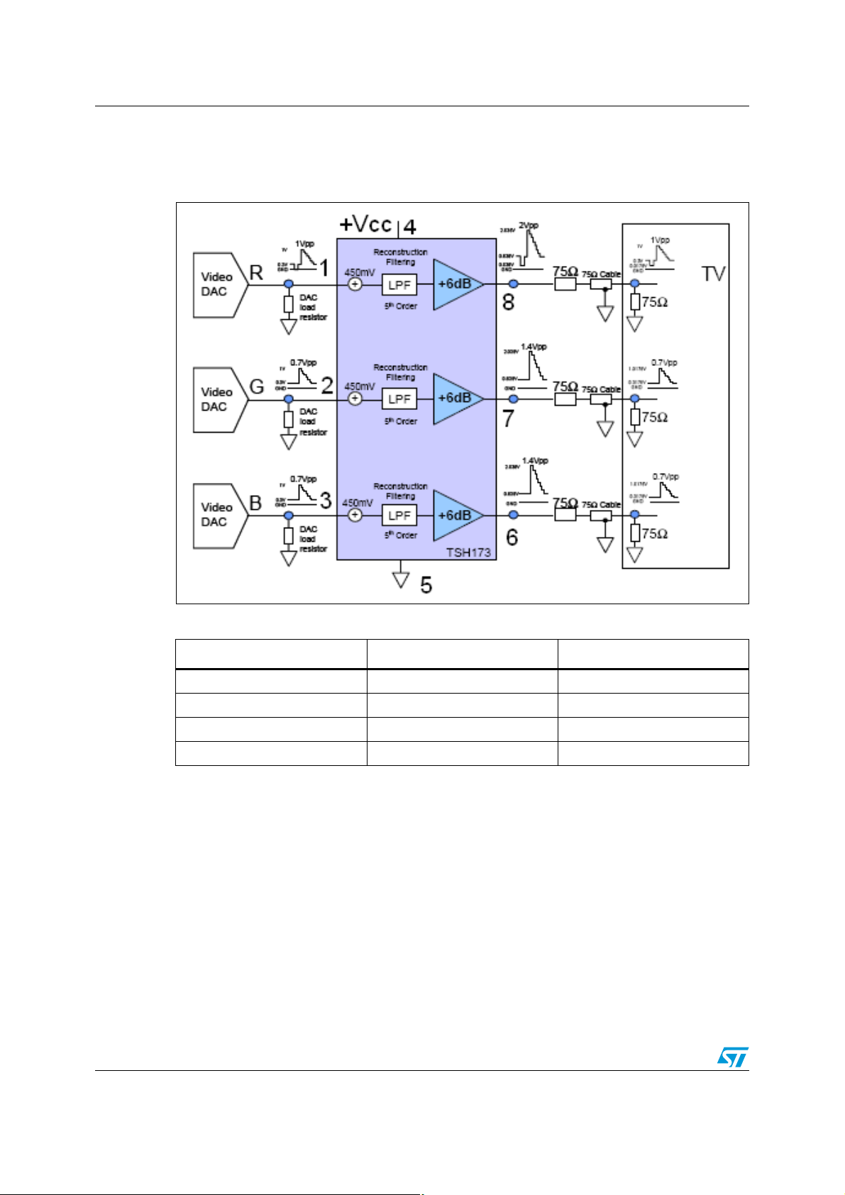
■ A short description of the TSH173 video buffer, including the internal block diagram
■ A description of the evaluation board and all of its components
■ The layout of the evaluation board
About the TSH173
The TSH173 is a single supply triple video buffer featuring an internal gain of 6dB and an
internal low pass filter of 8.2MHz cut-off frequency for each channel to fit with Standard
Definition requirements for video line interfaces.
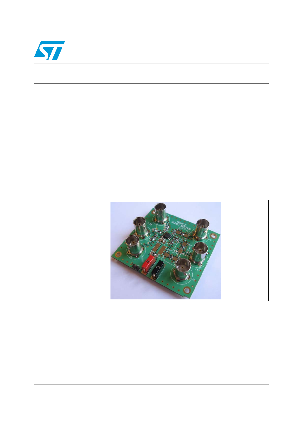
Figure 1. TSH173 evaluation board
Main features of the TSH173
– 4.5V to 5.5V single supply operation – No input capacitor required
– R-G-B, Y-Pb-Pr, Y-C-CVBS driving – Ve ry low harmonic distortion
– 3 channels with 6dB gain buffer – Each output can drive AC- or DC-coupled 150Ω loads
– 3 video reconstruction filters for SD – Tested on 5V power supply
– 3 internal input DC level shifter
January 2008 Rev 1 1/8
www.st.com
Page 2
TSH173 description AN2705
1 TSH173 description
Figure 2. TSH173 internal block diagram
Table 1. Pin description
Name Pin number Description
IN1, IN2, IN3 1, 2, 3 Input pins
OUT1, OUT2, OUT3 8, 7, 6 Output pins
+VCC 4 Positive supply
GND 5 Ground
2/8
Page 3
AN2705 Evaluation board description
2 Evaluation board description
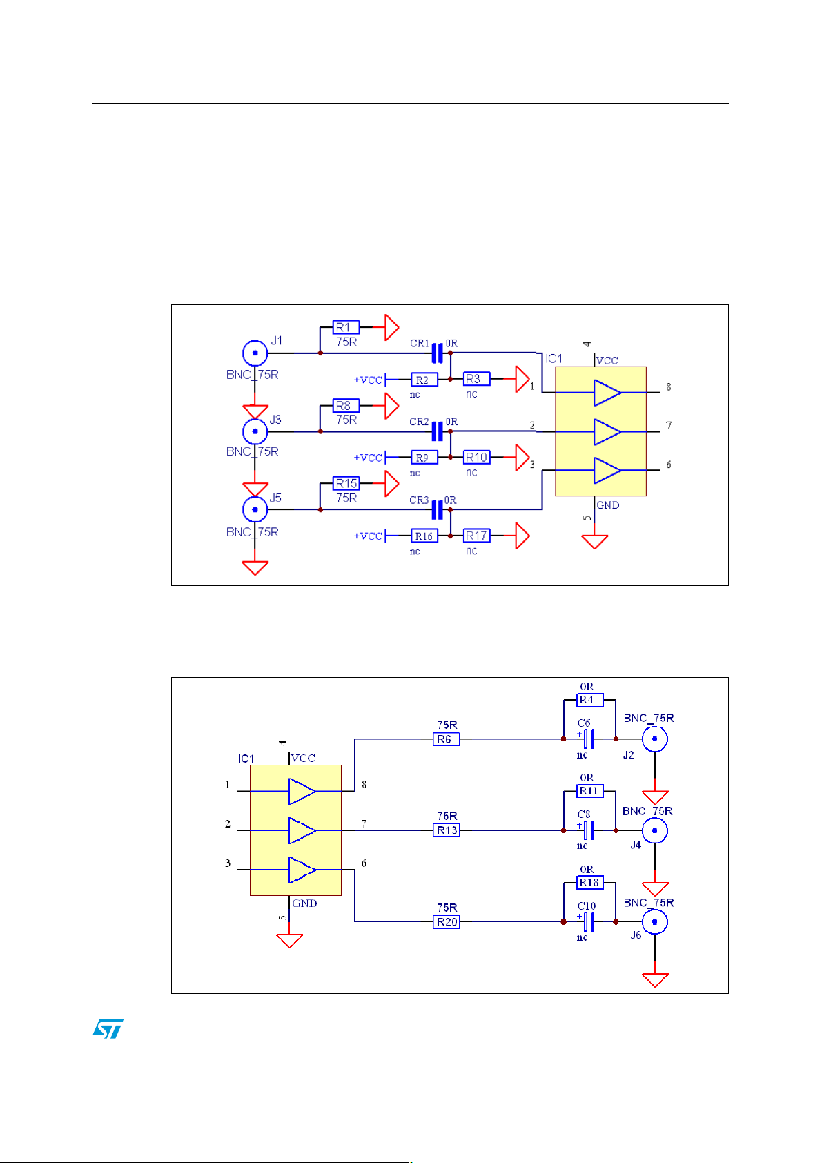
This board is designed to be tested with a 75Ω generator and 75Ω measurement tool.
Input signal must be between 0V and 1.4V so that it is not clamped. Otherwise, you must
replace the zero ohm resistor by a 100nF capacitor in CR1, CR2, and CR3, and add a
resistor bridge to polarize the input signal at the right level as shown in Figure 3. Resistor
bridge footprints are located on the back of the PCB.
Figure 3. TSH173 input
The TSH173 output can be AC coupled by a 220nF capacitor to minimize the DC
component on the line. To do this, you must remove the R4, R11, and R18 zero ohm
resistors and solder a 220µF capacitor on C6, C8, and C10 footprints as shown in Figure 4.
Figure 4. TSH173 AC output
3/8
Page 4

Evaluation board description AN2705
If you connect a system with an input impedance other than 75Ω to the PCB output, a Π
resistor footprint on the board allows you to match impedances.
For ex ample: you conn ect a scope with a 50Ω out put impedance. To match impedances, you
must add the following resistors: R5=2.2kΩ, R6=130Ω, R7=82Ω
The output can be AC or DC connected with this configuration.
Figure 5. TSH173 output impedance matching
Power supply
Correct power supply b ypassing is v ery important for optimizing perf ormance. A 10µF an d a
100nF are soldered on the board. This gives good performance. However, you can improve
it by adding a 100µF capacitor in C3 and placing a 560µH coil instead of the zero ohm
resistor in LR1.
Figure 6. Power supply
4/8
Page 5

AN2705 Schematic diagram and board components
3 Schematic diagram and board components
Figure 7. Board components
Figure 8. Full layout schematics
5/8
Page 6

Schematic diagram and board components AN2705
Table 2. List of board components
Part type Name on board Footprint Description
10 µF C1 1206 Bypass ceramic capacitor on V
100 µF C2 0805 Bypass ceramic capacitor on V
C3 8mm diameter
C4 0805
Bypass chemical capacitor on V
connected
Bypass ceramic capacitor on V
connected
CC
CC
CC
CC
not
not
0 ohm CR1, CR2, CR3 0805 Input capacitor replaced by a 0 ohm resistor
C6,C8,C10 Output capacitor 220µF not connected
TSH173 IC1 SO8
BNC 75Ω J1, J3, J5 BNC Input signal connectors
BNC 75Ω J2, J4, J6 BNC Output signal connectors
JACK J7, J8 Jack 2mm supply connectors
SIL J9 SIL SIL supply connector 2.54mm pitch
0 ohm LR1 1206 Coil replaced by 0 ohm resistor
75Ω R1, R8, R15 0805 input resistor
75Ω R6, R13, R20 0805 output resistor
R2, R3, R9, R10,
R16, R17
0805 Bridge resistors not connected
0 ohm R4, R11, R18 0805 Strap when output is DC coupled
R5, R7, R12,
R14, R19, R21
0805
Optional resistors to adapt output
impedance
6/8
Page 7

AN2705 PCB layout
4 PCB layout
Figure 9. Top layer Figure 10. Top layout
Figure 11. Bottom layer Figure 12. Bottom layout
5 Revision history
Table 3. Document revision history
31-Jan-2008 1 Initial release.
Date Revision Changes
7/8
Page 8

AN2705
Please Read Carefully:
Information in this document is provided solely in connection with ST products. STMicroelectronics NV and its subsidiaries (“ST”) reserve the
right to make changes, corrections, modifications or improvements, to this document, and the products and services described herein at any
time, without notice.
All ST products are sold pursuant to ST’s terms and conditions of sale.
Purchasers are solely res ponsibl e fo r the c hoic e, se lecti on an d use o f the S T prod ucts and s ervi ces d escr ibed he rein , and ST as sumes no
liability whatsoever relati ng to the choice, selection or use of the ST products and services described herein.
No license, express or implied, by estoppel or otherwise, to any intellectual property rights is granted under this document. If any part of this
document refers to any third pa rty p ro duc ts or se rv ices it sh all n ot be deem ed a lice ns e gr ant by ST fo r t he use of su ch thi r d party products
or services, or any intellectua l property c ontained the rein or consi dered as a warr anty coverin g the use in any manner whats oever of suc h
third party products or servi ces or any intellectual property contained therein.
UNLESS OTHERWISE SET FORTH IN ST’S TERMS AND CONDITIONS OF SALE ST DISCLAIMS ANY EXPRESS OR IMPLIED
WARRANTY WITH RESPECT TO THE USE AND/OR SALE OF ST PRODUCTS INCLUDING WITHOUT LIMITATION IMPLIED
WARRANTIES OF MERCHANTABILITY, FITNESS FOR A PARTICUL AR PURPOS E (AND THEIR EQUIVALE NTS UNDER THE LAWS
OF ANY JURISDICTION), OR INFRINGEMENT OF ANY PATENT, COPYRIGHT OR OTHER INTELLECTUAL PROPERTY RIGHT.
UNLESS EXPRESSLY APPROVED IN WRITING BY AN AUTHORIZED ST REPRESENTATIVE, ST PRODUCTS ARE NOT
RECOMMENDED, AUTHORIZED OR WARRANTED FOR USE IN MILITARY, AIR CRAFT, SPACE, LIFE SAVING, OR LIFE SUSTAINING
APPLICATIONS, NOR IN PRODUCTS OR SYSTEMS WHERE FAILURE OR MALFUNCTION MAY RESULT IN PERSONAL INJ URY,
DEATH, OR SEVERE PROPERTY OR ENVIRONMENTAL DAMAGE. ST PRODUCTS WHICH ARE NOT SPECIFIED AS "AUTOMOTIVE
GRADE" MAY ONLY BE USED IN AUTOMOTIVE APPLICATIONS AT USER’S OWN RISK.
Resale of ST products with provisions different from the statements and/or technical features set forth in this document shall immediately void
any warranty granted by ST fo r the ST pro duct or serv ice describe d herein and shall not cr eate or exten d in any manne r whatsoever , any
liability of ST.
ST and the ST logo are trademarks or registered trademarks of ST in various countries.
Information in this document su persedes and replaces all information previously supplied.
The ST logo is a registered trademark of STMicroelectronics. All other names are the property of their respective owners.
© 2008 STMicroelectronics - All rights reserved
STMicroelectronics group of compan ie s
Australia - Belgium - Brazil - Canada - China - Czech Republic - Finland - France - Germany - Hong Kong - India - Israel - Italy - Japan -
Malaysia - Malta - Morocco - Singapore - Spain - Sweden - Switzerland - United Kingdom - United States of America
www.st.com
8/8
 Loading...