


AN2692
Application note
How to program/reprogram the ST10F269Zx Flash memory
Introduction
This application note provides software guidelines and examples to program the
ST10F269Zx. More generally, this application note is applicable to any ST10 variant with an
0.35 µm technology embedded Flash memory.
The first section gives an overview of the ST10F269Zx embedded Flash memory’s key
features. It also shows the differences between the ST10F269Zx and ST10F168.
The second section describes how to develop software for the ST10F269Zx embedded
Flash memory through guidelines, examples and tips.
The last section is dedicated to embedded application aspects. More specifically, it gives
advices for Flash memory field reprogramming.
This application note does not replace the ST10F269Zx product datasheet. It refers to it and
it is necessary to have a copy of it to follow some of the explanations.
March 2008 Rev 1 1/29
www.st.com

Contents AN2692
Contents
1 Introduction to ST10F269Zx 0.35 µm embedded Flash memory . . . . . 6
1.1 Differences with ST10F168 . . . . . . . . . . . . . . . . . . . . . . . . . . . . . . . . . . . . 6
1.1.1 Single supply . . . . . . . . . . . . . . . . . . . . . . . . . . . . . . . . . . . . . . . . . . . . . . 6
1.1.2 New Erase/Program Controller . . . . . . . . . . . . . . . . . . . . . . . . . . . . . . . . 6
1.1.3 Improved granularity of block sizes . . . . . . . . . . . . . . . . . . . . . . . . . . . . . 6
1.2 Comparison with Standalone Flash memories . . . . . . . . . . . . . . . . . . . . . . 7
1.2.1 Similar but different erase/program commands . . . . . . . . . . . . . . . . . . . . 7
1.2.2 Description of the commands to the Flash memory Erase/Program
Controller . . . . . . . . . . . . . . . . . . . . . . . . . . . . . . . . . . . . . . . . . . . . . . . . . 7
1.2.3 Same Flash memory Status Register . . . . . . . . . . . . . . . . . . . . . . . . . . . 9
1.2.4 Boot block architecture . . . . . . . . . . . . . . . . . . . . . . . . . . . . . . . . . . . . . 10
1.2.5 Protection . . . . . . . . . . . . . . . . . . . . . . . . . . . . . . . . . . . . . . . . . . . . . . . . 10
1.2.6 Operating modes . . . . . . . . . . . . . . . . . . . . . . . . . . . . . . . . . . . . . . . . . . 11
2 Writing code for the ST10F269Zx with 0.35 µm embedded Flash . . . 12
2.1 ST10 programming constraints . . . . . . . . . . . . . . . . . . . . . . . . . . . . . . . . 12
2.1.1 Programming language . . . . . . . . . . . . . . . . . . . . . . . . . . . . . . . . . . . . . 12
2.2 Polling the Flash memory Erase/Program Controller . . . . . . . . . . . . . . . . 12
2.2.1 Ready/Busy signal . . . . . . . . . . . . . . . . . . . . . . . . . . . . . . . . . . . . . . . . . 12
2.2.2 Flash memory Status Register . . . . . . . . . . . . . . . . . . . . . . . . . . . . . . . 13
2.3 Flash memory mapping in the ST10F269Zx memory space . . . . . . . . . . 14
2.4 Program command . . . . . . . . . . . . . . . . . . . . . . . . . . . . . . . . . . . . . . . . . . 14
2.5 Erase commands . . . . . . . . . . . . . . . . . . . . . . . . . . . . . . . . . . . . . . . . . . . 16
2.6 Flash protection commands . . . . . . . . . . . . . . . . . . . . . . . . . . . . . . . . . . . 17
2.6.1 Set Block Protection . . . . . . . . . . . . . . . . . . . . . . . . . . . . . . . . . . . . . . . 17
2.6.2 Set Code Protection . . . . . . . . . . . . . . . . . . . . . . . . . . . . . . . . . . . . . . . . 17
2.7 Other Flash memory commands . . . . . . . . . . . . . . . . . . . . . . . . . . . . . . . 19
2.8 Tips to reduce Flash memory programming and erase times . . . . . . . . . 19
2.8.1 Reducing the programming time . . . . . . . . . . . . . . . . . . . . . . . . . . . . . . 19
2.8.2 Reducing erase times . . . . . . . . . . . . . . . . . . . . . . . . . . . . . . . . . . . . . . 19
3 Embedded application aspects . . . . . . . . . . . . . . . . . . . . . . . . . . . . . . . 21
3.1 Reading the Flash memory while erasing or programming . . . . . . . . . . . 21
2/29

AN2692 Contents
3.1.1 Minimum software to be copied into the on-chip RAM . . . . . . . . . . . . . . 21
3.1.2 Maximizing programming performance at system level . . . . . . . . . . . . . 21
3.1.3 Erase Suspend and Resume commands . . . . . . . . . . . . . . . . . . . . . . . 22
3.2 Field reprogramming with ST10F269Zx . . . . . . . . . . . . . . . . . . . . . . . . . . 22
3.2.1 Field events and Flash memory reliability . . . . . . . . . . . . . . . . . . . . . . . 22
3.2.2 Reset . . . . . . . . . . . . . . . . . . . . . . . . . . . . . . . . . . . . . . . . . . . . . . . . . . . 22
3.2.3 List of events and suggested handling methods . . . . . . . . . . . . . . . . . . 23
3.2.4 Generic aspects of Flash field reprogramming . . . . . . . . . . . . . . . . . . . 24
3.3 Ruggedized aspects . . . . . . . . . . . . . . . . . . . . . . . . . . . . . . . . . . . . . . . . . 25
3.3.1 Checksum . . . . . . . . . . . . . . . . . . . . . . . . . . . . . . . . . . . . . . . . . . . . . . . 25
3.3.2 Initialization of unused memory locations . . . . . . . . . . . . . . . . . . . . . . . 25
4 Quick summary . . . . . . . . . . . . . . . . . . . . . . . . . . . . . . . . . . . . . . . . . . . . 26
5 Conclusion . . . . . . . . . . . . . . . . . . . . . . . . . . . . . . . . . . . . . . . . . . . . . . . . 27
6 Revision history . . . . . . . . . . . . . . . . . . . . . . . . . . . . . . . . . . . . . . . . . . . 28
3/29

List of tables AN2692
List of tables
Table 1. Commands for ST10 with 0.35 µm embedded Flash memory . . . . . . . . . . . . . . . . . . . . . . . 7
Table 2. Flash memory block mapping (lower 32 Kbytes of memory) . . . . . . . . . . . . . . . . . . . . . . . 14
Table 3. Document revision history . . . . . . . . . . . . . . . . . . . . . . . . . . . . . . . . . . . . . . . . . . . . . . . . . 28
4/29

AN2692 List of figures
List of figures
Figure 1. Data polling flow . . . . . . . . . . . . . . . . . . . . . . . . . . . . . . . . . . . . . . . . . . . . . . . . . . . . . . . . . 13
Figure 2. Verification algorithm for word programming . . . . . . . . . . . . . . . . . . . . . . . . . . . . . . . . . . . 14
Figure 3. Verification algorithm for erasing . . . . . . . . . . . . . . . . . . . . . . . . . . . . . . . . . . . . . . . . . . . . 16
5/29

Introduction to ST10F269Zx 0.35 µm embedded Flash memory AN2692
1 Introduction to ST10F269Zx 0.35 µm embedded Flash
memory
This section describes the improvements made from the ST10F168 and the differences with
standalone Flash memories.
1.1 Differences with ST10F168
1.1.1 Single supply
ST10 variants with 0.35 µm embedded Flash memories do not require specific a supply for
programming. On-chip charge pumps provide the necessary supply from the external single
5 V supply.
1.1.2 New Erase/Program Controller
The 0.35 µm Erase/Program Controller was changed to be more similar to the one of
standalone Flash memories: erasing and programming of Flash memory cells is no more
done by the ST10. This allows:
● Savings on system stack: Space no longer needs allocated on the ST10 system
stack for erasing and programming,
● Improved efficiency during programming: ST10 CPU can be used to handle
communication during the time where the Erase/Program Controller is dealing with the
Flash memory
● Improved clock scheme: the Flash Erase/Program Controller has its own clock; there
is no more need to specify it to the CPU clock. This also simplifies the handling of
special events (like PLL unlock) during erasing/programming.
1.1.3 Improved granularity of block sizes
The ST10F269Zx 0.35 µm embedded Flash memory has an improved block granularity
(smaller blocks) and also features a boot block organization:
● Block size is 64 Kbytes for standard blocks,
● Small blocks for the 4 boot blocks (16 Kbyte, then 8 Kbyte, 8 Kbyte, 32 Kbyte).
6/29
AN2692 Introduction to ST10F269Zx 0.35 µm embedded Flash memory
1.2 Comparison with Standalone Flash memories
1.2.1 Similar but different erase/program commands
The Erase/Program Controller of ST10F269Zx is derived from the Common Flash memory
Interface:
● To keep the same level of proven safety, the special sequence of commands of
standalone Flash memories has been kept,
● To differentiate embedded Flash memories from external Flash memories, the value of
the commands (addresses and data) have been slightly modified.
1.2.2 Description of the commands to the Flash memory Erase/Program Controller
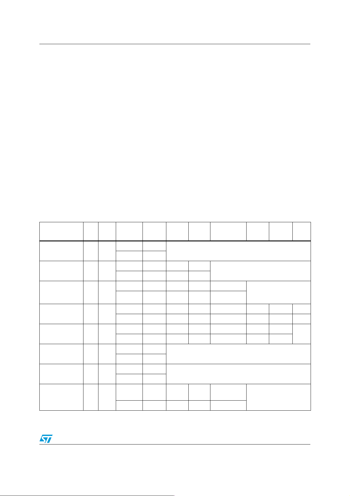
Ta bl e 1 describes the commands allowed with the ST10F269Zx Erase/Program Controller.
Commands to the Flash memory are defined by a sequence of ST10F269Zx write cycles
with specific addresses and data within the Flash memory address range. The length of the
sequence varies from 1 cycle (e.g.: Read/Reset) to 6 cycles (Chip Erase).
The Block Erase command can be extended by 1 cycle per additional block to erase. This
translates in a maximum of 12 cycles for the ST10F269Zx.
Table 1. Commands for ST10 with 0.35 µm embedded Flash memory
Instruction Mne Cycle
Read/Reset RD 1+
Address/
Data
(2)
Addr.
st
1
cycle
X
2nd
cycle
3rd
cycle
th
4
Read Memory Array until a new write cycle is initiated
Data xxF0h
(2)
Read/Reset RD 3+
Addr.
Data xxA8h xx54h xxF0h
Addr.
x1554h x2AA8h xxxxxh
Read Memory Array until a new write
cycle is initiated
(2)
x1554h x2AA8h x1554h WA Read Data Polling or
Program Word PW 4
Data xxA8h xx54h xxA0h WD
(2)
Addr.
x1554h x2AA8h x1554h x1554h x2AA8h BA BA’
Block Erase BE 6
Data xxA8h xx54h xx80h xxA8h xx54h xx30h xx30h
(2)
Addr.
x1554h x2AA8h x1554h x1554h x2AA8h x1554h
Chip Erase CE 6
Data xxA8h xx54h xx80h xxA8h xx54h xx10h
(2)
Erase Suspend ES 1
Erase Resume ER 1
Addr.
Data xxB0h
(2)
Addr.
Data xx30h
X
Read until Toggle stops, then read or program all data
needed from block(s) not being erased then Resume Erase.
X
Read Data Polling or Toggle bit until Erase completes or
Erase is suspended another time.
cycle
(1)
th
5
6th
cycle
cycle
Toggle bit until program
completes.
7th
cycle
(3)
Note
(4)
Set Block/Code
Protection
SP 4
Addr.
(2)
x2A54h x15A8h x2A54h
Any odd word
address
Data xxA8h xx54h xxC0h WPR
7/29
(5)
(6)
Introduction to ST10F269Zx 0.35 µm embedded Flash memory AN2692
cycle
(1)
(continued)
th
5
6th
cycle
Read Protection Register
(5)
until a new write cycle is
cycle
initiated.
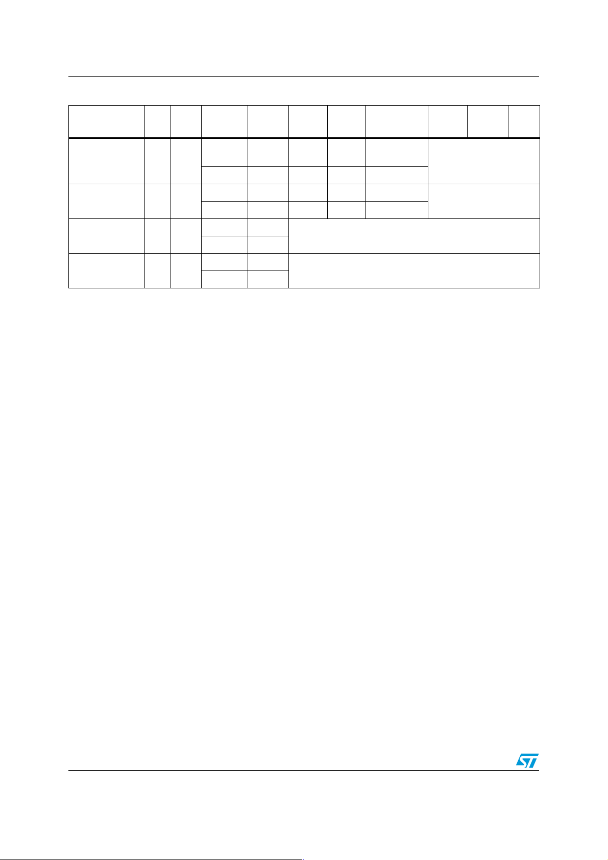
Table 1. Commands for ST10 with 0.35 µm embedded Flash memory
Instruction Mne Cycle
Read Protection
Status
RP 4
Address/
Data
(2)
Addr.
Data xxA8h xx54h xx90h Read PR
(2)
Block Temporary
Unprotection
Code Temporary
Unprotection
Code Temporary
Protection
1. Mne = mnemonic, X = Don’t Care.
WA = Write Address: address of memory location to be programmed.
WD = Write Data: 16-bit data to be programmed.
BA = Block address.
2. Address bit A14, A15 and above are don’t care for coded address inputs.
3. Optional, additional blocks addresses must be entered within a timeout delay (96 µs) after last write entry, timeout status
can be verified through FSB.3 value. When full command is entered, read Data Polling or Toggle bit until Erase is
completed or suspended.
4. Read data polling or toggle bit until erase completes.
5. Odd word address = 4n-2 where n = 0, 1, 2, 3..., e.g. 0002h, 0006h, etc.
6. WPR = Write protection register. To protect code, bit 15 of WPR must be ‘0’. To protect block N (N=0,1,...), bit N of WPR
must be ‘0’. Bit that are already at ‘0’ in protection register must also be ‘0’ in WPR, else a writing error will occurs (it is not
possible to write a ‘1’ in a bit already programmed at ‘0’).
7. MEM = any address inside the Flash memory space. Absolute addressing mode must be used (MOV MEM, Rn), and
instruction must be executed from Flash memory space.
BTU 4
CTU 1
CTP 1
Addr.
Data xxA8h xx54h xxC1h xxF0h
(2)
Addr.
Data FFFFh
(2)
Addr.
Data FFFBh
st
1
cycle
x2A54h x15A8h x2A54h
2nd
cycle
3rd
cycle
th
4
Any odd word
address
x2A54h x15A8h x2A54h X
(7)
MEM
Write cycles must be executed from Flash.
(7)
MEM
Write cycles must be executed from Flash.
7th
cycle
Flash commands and ST10 pipeline effect
Due to the ST10F269Zx pipeline effect, all erase and program commands must not be
immediately followed by a JMPx, CALLx or RETx instruction.
For any erase or program command, a NOP instruction must be inserted after sending the
last command to the Flash memory Erase/Program Controller.
When not implemented, and when the ST10F269Zx is in bootstrap mode with the code
running from the XRAM or an external memory, the TestFlash may be selected instead of
the user Flash memory (for details, please refer to ST10F269Zx errata sheet).
8/29

AN2692 Introduction to ST10F269Zx 0.35 µm embedded Flash memory
1.2.3 Same Flash memory Status Register
The Flash memory Status Register is used to flag the status of the Flash memory and the
result of an operation.
To maximize the reuse of Flash memory programming software, the Flash memory Status
Register of standalone Flash memories has been kept.
This register can be accessed by read cycles during Program/Erase Controller (P/E.C.)
operations. Erase/program operations can be controlled by data polling on the FSB7 bit of
the Status Register. Toggle detection is indicated on FSB6 and FSB2, error on FSB5 and
erase timeout on the FSB3 bit. Any read attempt from the Flash memory during an erase or
a program operation will automatically output these five bits. The P/E.C. sets bits FSB2,
FSB3, FSB5, FSB6 and FSB7. Other bits are reserved for future use and should be
masked.
Flash memory Status
Note: The address of the Flash memory Status Register is the address of the word being
programmed when a programming operation is in progress, or an address within the block
being erased when an erasing operation is in progress.
15 14 13 12 11 10 9 8 7 6 5 4 3 2 1 0
--------FSB.7FSB.6FSB.5-FSB.3FSB.2--
FSB.7 bit Flash Status Bit 7: Data Polling bit
FSB.6 bit Flash Status Bit 6: Toggle bit
FSB.5 bit Flash Status Bit 5: Error bit
FSB.3 bit Flash Status Bit 3: Erase Timeout bit
RRR RR
Programming operation: this bit outputs the complement of the bit 7 of the word being programmed,
and after completion, will output the bit 7 of the programmed word.
Erasing operation: outputs a ‘0’ during erasing, and ‘1’ after erasing completion.
If the block(s) selected for erasure is (are) protected, FSB.7 is set to ‘0’ for about 100 µs, and then
returns to the previous addressed memory data value.
FSB.7 also flags the Erase Suspend mode by switching from ‘0’ to ‘1’ at the start of Erase Suspend.
During program operation in Erase Suspend mode, FSB.7 has the same behavior as in normal
program execution outside the Erase Suspend mode.
Programming or erasing operations: successive read operations of Flash Status register deliver
complementary values. FSB.6 toggles each time the Flash Status Register is read. The program
operation is completed when two successive reads yield the same value. The next read will output
the last programmed bit, or a ‘1’ after an erase operation
FSB.6 is set to‘1’ if a read operation is attempted on an Erase Suspended block. In addition, an
Erase Suspend/Resume command will cause FSB.6 to toggle.
This bit is set to ‘1’ when there is a failure of a program, Block or Chip Erase operation.This bit is
also set if a user tries to program a bit to ‘1’ to a Flash memory location that is currently
programmed with ‘0’.
The error bit is reset after a Read/Reset command.
In case of success, the Error bit is set to ‘0’ during Program or Erase and then outputs the last
programmed bit or a ‘1’ after erasing
This bit is set to ‘1’ by the P/E.C. when the last Block Erase command has been entered to the
Command Interface and is awaiting the erase start. When the timeout period is finished, after
96 µs, FSB.3 returns to ‘1’.
9/29
 Loading...