

Page 1

AN2689
Application note
Protection of automotive electronics from electrical hazards,
guidelines for design and component selection
Introduction
Electronic equipment represents a large part of the automobiles of today. Although these
electronic modules bring much more comfort and security for the vehicle user, they also
bring significant concerns in terms of reliability regarding the automobile environment.
Because electronic modules are sensitive to electromagnetic disturbances (EMI),
electrostatic discharges (ESD) and other electrical disturbances (and automobiles are the
source of many such hazards), caution must be taken wherever electronic modules are
used in the automotive environment.
Several standards have been produced to model the electrical hazards that are currently
found in automobiles. As a result manufacturers and suppliers have to consider these
standards and have to add protection devices to their modules to fulfill the major obligations
imposed by these standards.
The objective of this document is to help electronic module designers with a protection
design approach for selecting the most suitable devices for typical applications depending
on the protection standard the electronic module has to meet.
Section 1 describes the electrical hazards considered in this document. Section 2 presents
a list of parameters to be taken into account before selecting possible protection devices.
Section 3 and Section 4 provide worked design examples, with design calculations, for
several protection solutions. Section 5 provides recommendations for the design of PCB
layout for improved solutions.
Transil is a trademark of STMicroelectonics.
March 2010 Doc ID 14310 Rev 2 1/41
www.st.com
Page 2

AN2689
Contents
1 Electrical hazards in the automotive environment . . . . . . . . . . . . . . . . . 4
1.1 Source of hazards . . . . . . . . . . . . . . . . . . . . . . . . . . . . . . . . . . . . . . . . . . . 4
1.1.1 Conducted hazards . . . . . . . . . . . . . . . . . . . . . . . . . . . . . . . . . . . . . . . . . 4
1.1.2 Radiated hazards . . . . . . . . . . . . . . . . . . . . . . . . . . . . . . . . . . . . . . . . . . . 4
1.2 Propagation of electrical hazards . . . . . . . . . . . . . . . . . . . . . . . . . . . . . . . . 5
1.2.1 Propagation on the data lines . . . . . . . . . . . . . . . . . . . . . . . . . . . . . . . . . 5
1.2.2 Hazards on the supply rail . . . . . . . . . . . . . . . . . . . . . . . . . . . . . . . . . . . . 6
1.3 Standards for the protection of automotive electronics . . . . . . . . . . . . . . . 7
2 Parameters to consider in selecting protection devices . . . . . . . . . . . . 8
3 Data line protection . . . . . . . . . . . . . . . . . . . . . . . . . . . . . . . . . . . . . . . . . 9
3.1 Protection topologies . . . . . . . . . . . . . . . . . . . . . . . . . . . . . . . . . . . . . . . . . 9
3.1.1 Clamping topology . . . . . . . . . . . . . . . . . . . . . . . . . . . . . . . . . . . . . . . . . . 9
3.1.2 Rail-to-rail topology . . . . . . . . . . . . . . . . . . . . . . . . . . . . . . . . . . . . . . . . 10
3.2 Data line protection example . . . . . . . . . . . . . . . . . . . . . . . . . . . . . . . . . . 12
3.3 Design calculation example . . . . . . . . . . . . . . . . . . . . . . . . . . . . . . . . . . . 14
3.3.1 Determination of Rd . . . . . . . . . . . . . . . . . . . . . . . . . . . . . . . . . . . . . . . . 14
3.3.2 Power dissipation determination . . . . . . . . . . . . . . . . . . . . . . . . . . . . . . 16
4 Supply rail protection . . . . . . . . . . . . . . . . . . . . . . . . . . . . . . . . . . . . . . . 21
4.1 Protection topology . . . . . . . . . . . . . . . . . . . . . . . . . . . . . . . . . . . . . . . . . . 21
4.1.1 Clamping topology . . . . . . . . . . . . . . . . . . . . . . . . . . . . . . . . . . . . . . . . . 21
4.2 Supply rail protection example 1: pulse 2 ISO 7637-2 . . . . . . . . . . . . . . . 21
4.3 Calculations for example 1 . . . . . . . . . . . . . . . . . . . . . . . . . . . . . . . . . . . . 23
4.3.1 Determination of R
4.3.2 Power dissipation determination . . . . . . . . . . . . . . . . . . . . . . . . . . . . . . 24
4.3.3 Junction temperature determination . . . . . . . . . . . . . . . . . . . . . . . . . . . 26
4.4 Supply rail protection example 2: pulse 5a load dump ISO 7637-2 . . . . . 28
4.5 Calculations for example 2 . . . . . . . . . . . . . . . . . . . . . . . . . . . . . . . . . . . . 29
d . . . . . . . . . . . . . . . . . . . . . . . . . . . . . . . . . . . . . . . . . . . . . . . . . . . 23
4.5.1 Determination of Rd . . . . . . . . . . . . . . . . . . . . . . . . . . . . . . . . . . . . . . . . 30
4.5.2 Power dissipation determination . . . . . . . . . . . . . . . . . . . . . . . . . . . . . . 31
5 PCB layout recommendations . . . . . . . . . . . . . . . . . . . . . . . . . . . . . . . . 33
2/41 Doc ID 14310 Rev 2
Page 3

AN2689
5.1 Parasitic inductances of the Transil and the PCB tracks . . . . . . . . . . . . . 33
5.1.1 Parasitic inductance from Transil wiring . . . . . . . . . . . . . . . . . . . . . . . . . 33
5.1.2 Capacitive and inductive coupling . . . . . . . . . . . . . . . . . . . . . . . . . . . . . 37
5.1.3 Parasitic coupling due to the loop-effect . . . . . . . . . . . . . . . . . . . . . . . . 39
6 Conclusion . . . . . . . . . . . . . . . . . . . . . . . . . . . . . . . . . . . . . . . . . . . . . . . . 40
7 Revision history . . . . . . . . . . . . . . . . . . . . . . . . . . . . . . . . . . . . . . . . . . . 40
Doc ID 14310 Rev 2 3/41
Page 4
Electrical hazards in the automotive environment AN2689
1 Electrical hazards in the automotive environment
The automotive environment is the source of many electrical hazards. These hazards, such
as electromagnetic interference, electrostatic discharges and other electrical disturbances
are generated by various accessories like ignition, relay contacts, alternator, injectors,
SMPS (i.e. HID front lights) and other accessories.
These hazards can occur directly in the wiring harness in case of conducted hazards, or be
applied indirectly to the electronic modules by radiation. These generated hazards can
impact the electronics in two ways - either on the data lines or on the supply rail wires,
depending on the environment.
1.1 Source of hazards
1.1.1 Conducted hazards
These hazards occur directly in the cable harness. They are generated by inductive loads
like electro-valves, solenoids, alternators, etc.
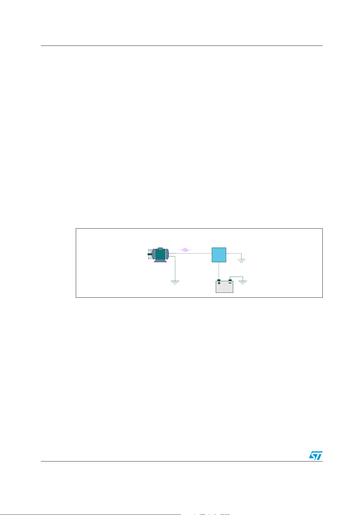
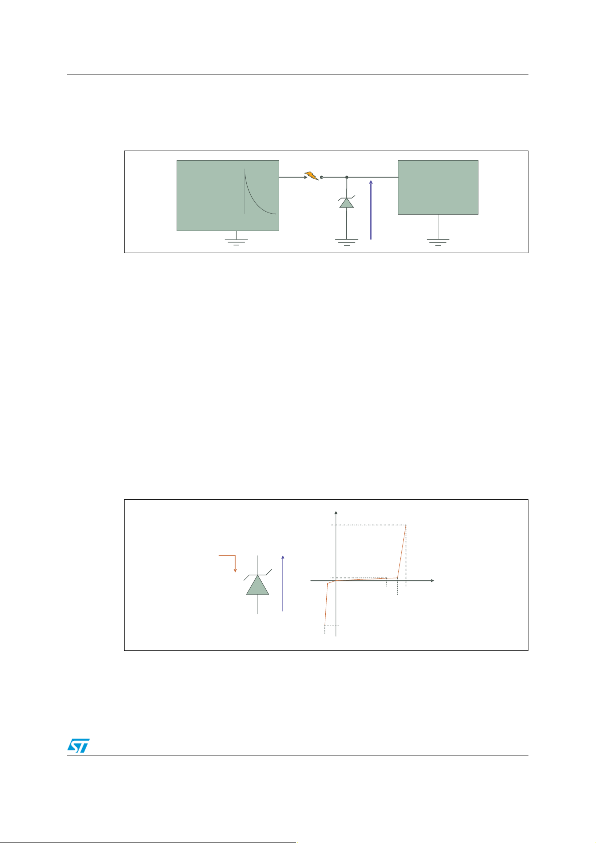
The schematic in Figure 1 shows a typical configuration.
Figure 1. Conducted hazards
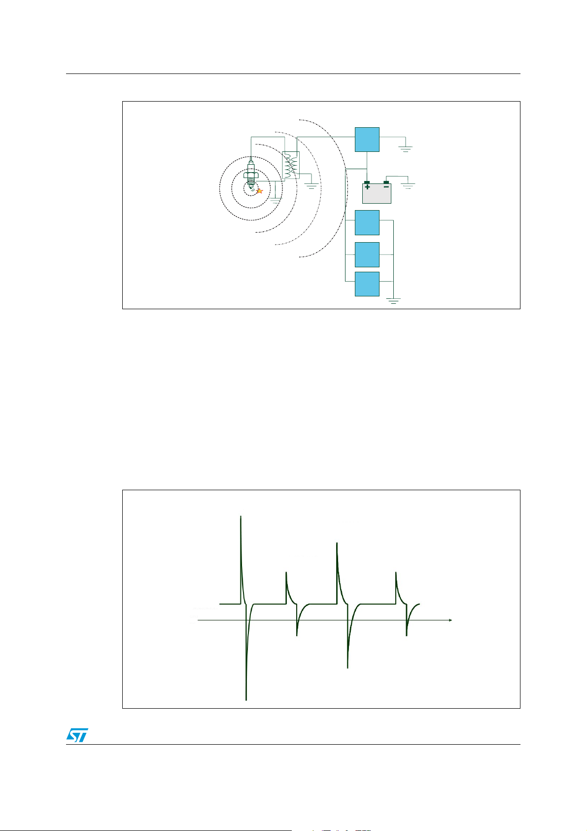
1.1.2 Radiated hazards
These hazards are generated by high current switching like relay contact, high current MOS
or IGBT switches, ignition systems, etc. The electromagnetic field generated by these
circuits directly affects lines or modules near the source of the electromagnetic radiation.
The schematic diagram in Figure 2 indicates how electromagnetic radiation creates such
hazards as electromagnetic interference in electronic modules.
Source of
distrubances
Alternator
Equipment
needing protection
ECU
Battery
4/41 Doc ID 14310 Rev 2
Page 5
AN2689 Electrical hazards in the automotive environment
Figure 2. Electromagnetic radiation in the automotive environment
Equipment
needing protection
Ignition coil
Spark
plug
1.2 Propagation of electrical hazards
1.2.1 Propagation on the data lines
Transients that are generated on data lines are mainly ESD surges which are low energy but
very high dv/dt and can generate a very strong electromagnetic field. These mainly concern
ISO 10605 and IEC 61000-4-2 standards.
ECU
Battery
ABS
CAR
RADIO
...
The data lines concerned are communication lines like media transfer lines, data buses,
sensor data lines and so on.
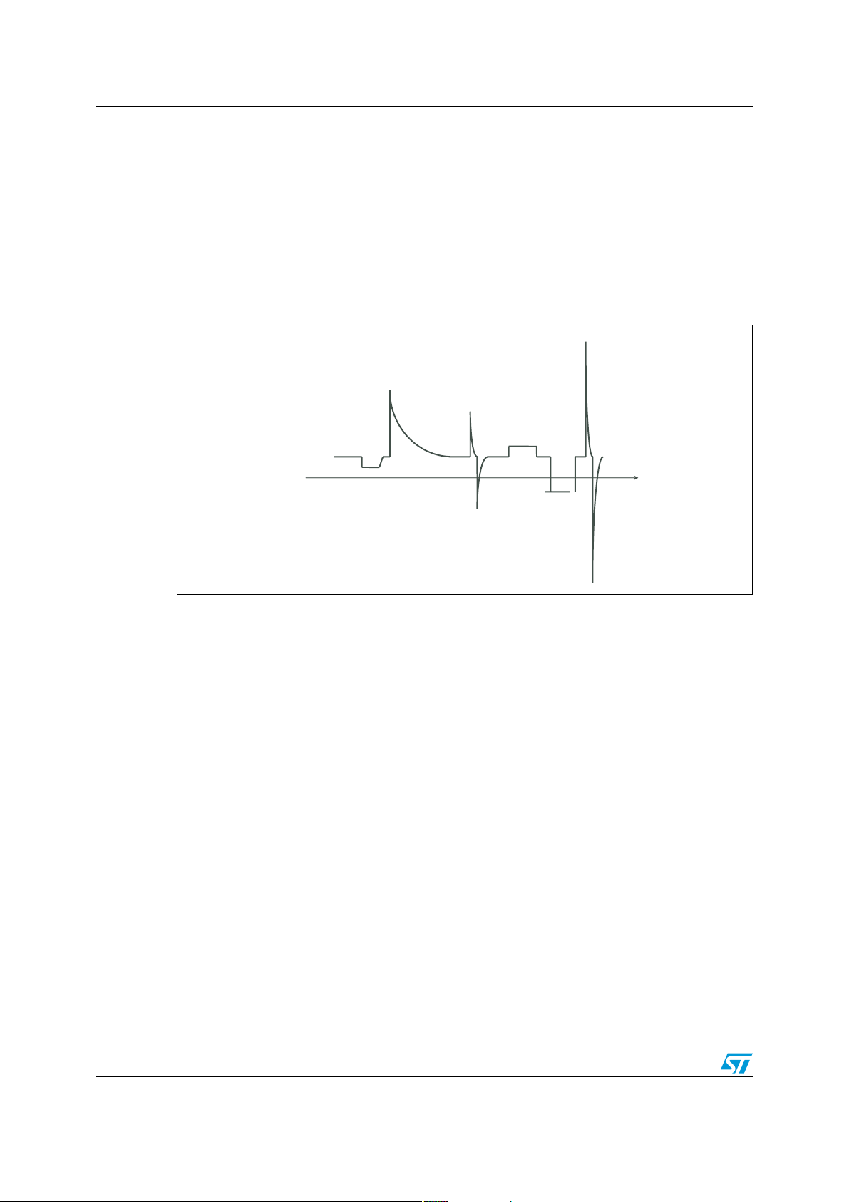
Figure 3 shows surge forms of hazards that can be found on data lines.
Figure 3. Kinds of surges on data lines
±25 kV (1)
ISO 10605
±15 kV (1)
IEC 61000-4-2
±8 kV (2)
ISO 10605
Nominal
V dataline
0V
±8 kV (2)
IEC 61000-4-2
(1): Air discharge
(2): Contact discharge
Doc ID 14310 Rev 2 5/41
Page 6
Electrical hazards in the automotive environment AN2689
The ISO 10605 ESD surge test is applied to a complete system. This is simulating the ESD
occurring on an electronic module in its environment due to human body contact.
1.2.2 Hazards on the supply rail
Transients that are generated on the supply rail range from severe low level-high energy, to
high level-low energy with sometimes high dv/dt. These mainly concern ISO 7637-2 and ISO
10605 standards.
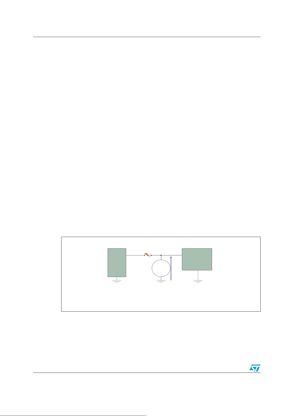
Figure 4 shows a simple representation of the form of major supply rail transients.
Figure 4. Kinds of surges on power rail
±25 kV
ESD spikes
87 V
Load dump
Nominal
14 V
0V
6 VCrank
+100/-150V
Spikes
24 VJump start
Reverse battery
The most energetic transients are those resulting from load-dump and jump start. But all
other hazards may affect the normal operation of electronic modules.
The “6 V crank” is caused by the starting of the car. The energy necessary to crank the
engine makes the power voltage drop to 6 V.
The load-dump is caused by the discharged battery being disconnected from the alternator
while the alternator is generating charging current. This transient can last 400 ms and the
equivalent generator internal resistance is specified as 0.5 Ω minimum to 4 Ω maximum.
The “+100/-150 V Spikes” are due to the ignition system that is necessary to ignite the
gasoline mixture. The frequency of the spikes depends on the engine rotation speed and the
number of cylinders. These generate electromagnetic radiation.
The “24 V jump start” results from the temporary application of an over voltage in excess of
the battery voltage. The circuit power supply may be subjected to a temporary over voltage
condition due to the regulator failing or deliberately generated when it is necessary to boost
start the car. In such condition some repair vehicles use 24 V battery jump to start the car.
Automotive specifications call for the support of this over voltage application for up to 5
minutes.
The “reverse battery” is the result of battery inversion by mistake. Thus accessories have
their power termination polarized in the wrong way.
The “25 kV ESD spike” is the result of electrostatic discharge (ESD)
All these events may affect the electronic environment as conducted hazards or as radiated
hazards.
6/41 Doc ID 14310 Rev 2
Page 7

AN2689 Electrical hazards in the automotive environment
1.3 Standards for the protection of automotive electronics
All the hazards indicated above are described by several standards bodies such as the
Society of Automobile Engineers (SAE), the Automotive Electronic Council (AEC) and the
International Standard Organization (ISO ).
Because the ISO 10605
(a)
and the ISO 7637
standards regarding electrical hazards, this document mainly concerns the cases
considering such standards.
(b)
are the most important automotive
a. ISO 10605: standard for “Electrostatic discharges” due to human body discharging inside a vehicle applied to a
complete system
b. ISO 7637 standard for “Electrical disturbances from conduction and coupling
Doc ID 14310 Rev 2 7/41
Page 8
Parameters to consider in selecting protection devices AN2689
2 Parameters to consider in selecting protection
devices
To make the best choice in protection device and considering Figure 5, it is necessary to
consider several parameters such as:
● Nominal voltage the electronic module runs with (V
● Maximum voltage this electronic module can support (V
● Kind of surge that the electronic module may be called upon to support
– If the surge shape is exponential:
What is the surge maximum voltage (V
)?
s
What is the surge duration and at what level is it measured (t
What is the surge generator impedance (R
s
What is the number of cycles in the surge (1/f)?
– If the surge is a dc surge:
What is the dc voltage level (V
What is the duration of the surge (t
What is the surge generator impedance (R
● What is the ambient temperature (T
● What kind of protection package is preferred?
● Is the electronic module a simple dc module or a digital one?
dc
amb
)?
)?
)?
p
s
– If digital:
What is the signal frequency (F)?
What are the rise and fall time of the surge signal (t
What is the maximum line capacitance (C
)?
l
)?
)?
nom
)
max
, tf)?
r
)
)?
p
Figure 5. Surge application topology
Surge
Generator
Vs
Rs
Td
F
(*) Transil
8/41 Doc ID 14310 Rev 2
Protection
device (*)
or rail-to-rail protection device
Module to protect
Vcl
Vnom
Vmax
Page 9
AN2689 Data line protection
3 Data line protection
3.1 Protection topologies
3.1.1 Clamping topology
Various protection topologies can be chosen for data line protection. There is the usual
topology that consists of using a clamping device as shown in Figure 6. The action of the
suppressor upon positive and negative surge occurrence is shown respectively in Figure 7
and Figure 8.
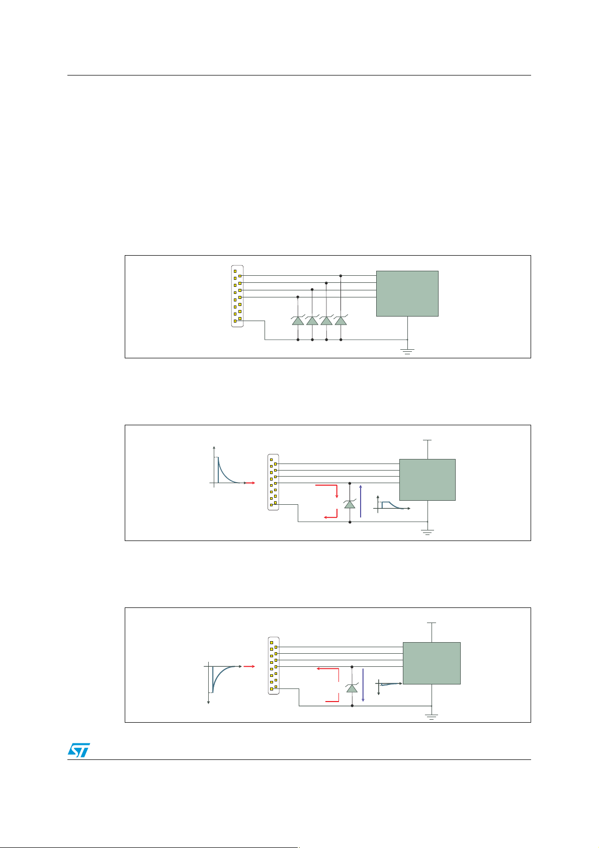
Figure 6. Data line protection using Transils
Module to protect
Sensitiveline
Vnom
Vmax
Accessory Connector
Transil
When a positive surge occurs, the over voltage is suppressed by the Transil as the voltage
passes the breakdown voltage (Vbr). Thus the current is diverted to ground. The remaining
voltage on the data line is limited to the clamping voltage (V
).
cl
Figure 7. Positive surge suppression
Vcc
Vs
Module to protect
Vnom
Sensitivedatalines
Accessory Connector
I
Vcl
Vmax
For the negative surge, the Transil is now in forward mode and the over voltage is eliminated
as the surge voltage passes the forward voltage drop of the protection device (V
remaining voltage is limited to the peak forward voltage of the Transil (V
).
fp
). The
f
Figure 8. Negative surge suppression
Vcc
Module to protect
Vnom
Sensitivedatalines
Vs
Accessory Connector
I
Vfp
Vmax
Doc ID 14310 Rev 2 9/41
Page 10
Data line protection AN2689
This topology is easy to manage. There should be as many protection devices as there are
lines to protect. The protection device in fact can be several single Transils but there is a
possibility to use protection devices in an array package so that one device protects each
data line as shown in Figure 9.
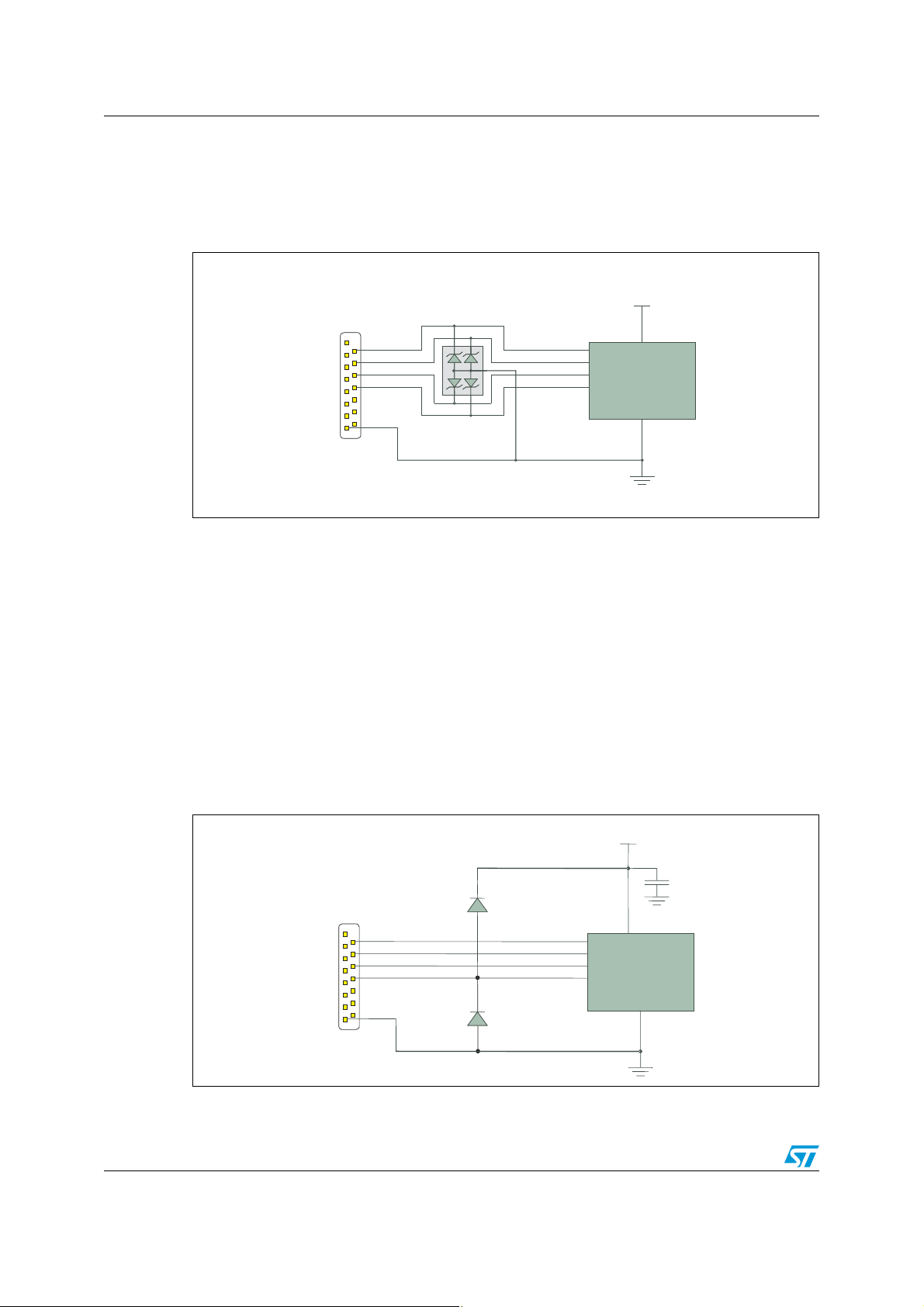
Figure 9. Data line protection using a diode array
Vcc
Transilarray
Module to protect
Sensitiveline
Accessory Connector
Vnom
Vmax
This clamping topology is good when the clamping voltage of each Transil is close to the
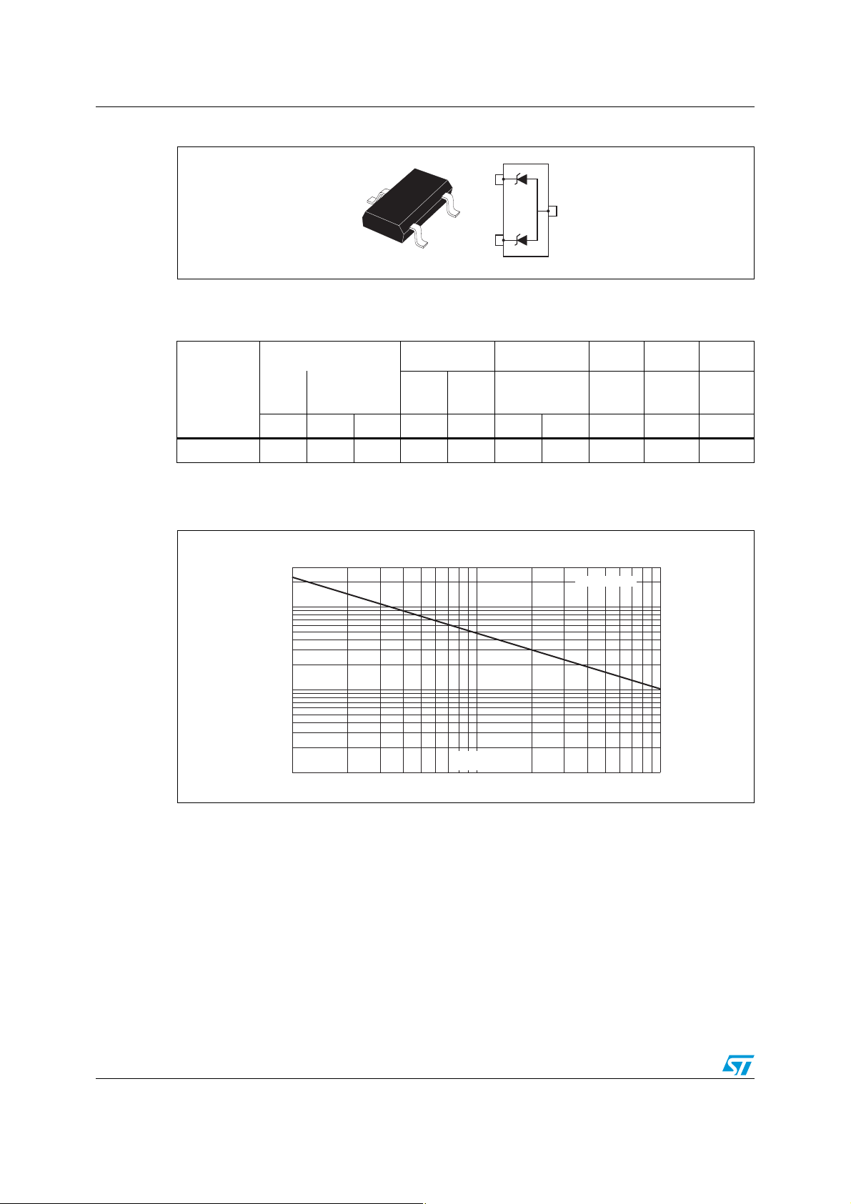
nominal voltage of the data lines to be protected. For example, if the nominal voltage is 5 V,
an ESDA6V1xx (V
= 6.1 V) protection device is ideal. The Transil offers a fixed clamping
br
voltage which does not require external power supply as in the rail-to-rail configuration but
for some cases it is more convenient to use the rail-to-rail topology as described below.
3.1.2 Rail-to-rail topology
The rail-to-rail topology, shown in Figure 10, is achieved using simple regular diodes. In that
case the clamping level is no longer fixed but, instead, depends on the power supply voltage
V
. As soon as a surge occurs, all the voltage over Vcc is diverted to the power supply as
cc
shown in Figure 11.
In this case the remaining over voltage that the data line is exposed to is very low.
Figure 10. Rail-to-rail protection topology
Connector
Accessory
Vcc
lines
Module to protect
Sensi t i ve dat a
Vnom
Vmax
10/41 Doc ID 14310 Rev 2
Page 11
AN2689 Data line protection
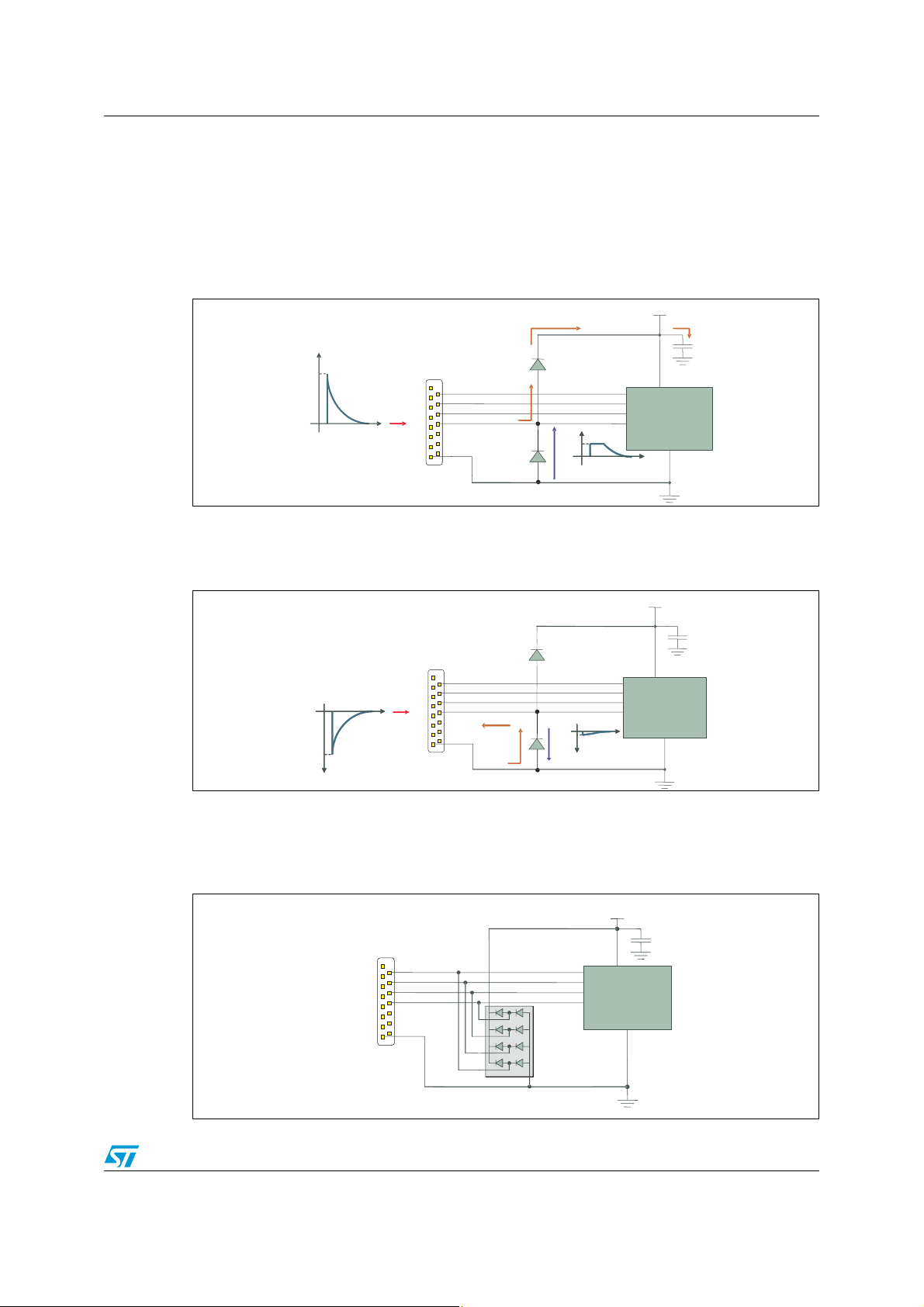
For a positive surge, shown in Figure 11, as the over voltage reaches the power supply
voltage V
plus the forward voltage drop of the upper diode, the surge current is diverted
cc
into the power supply line. To prevent this power supply line oscillating or being raised too
much, a capacitor (47 nF suggested) is needed close to the rail-to-rail protection device.
The remaining voltage V at the module data line is limited to Vcc plus the forward voltage
drop V
of the upper diode.
f
Figure 11. Positive surge suppression
Isurge
Vs
Sensitivedata lines
Accessory Connector
V
Vcc
Module to protect
Vnom
Vmax
For the negative surge case (Figure 12), the surge suppression is the same as described in
Figure 8.
Figure 12. Negative surge suppression
Vcc
Module to protect
Isurge
Sensitivedata lines
Vs
Accessory Connector
V
Vnom
Vmax
In the same approach as for the previous topology, there is a possibility to manage this railto-rail protection topology using as many single devices as there are data lines to protect or
one diode array device that fulfills all line protection needs as shown in Figure 13.
Figure 13. Rail-to-rail diode array
Vcc
lines
Connector
Sensi t i ve dat a
Module to protect
Vnom
Vmax
Accessory
DiodeArray
Doc ID 14310 Rev 2 11/41
Page 12
Data line protection AN2689
This solution requires that the Vcc voltage track be accessible and a decoupling capacitor is
required close to the diode array device. On the other hand this topology is suitable for high
speed data lines that often requires low parasitic line capacitance.
3.2 Data line protection example
Let’s consider the ISO 10605 standard.
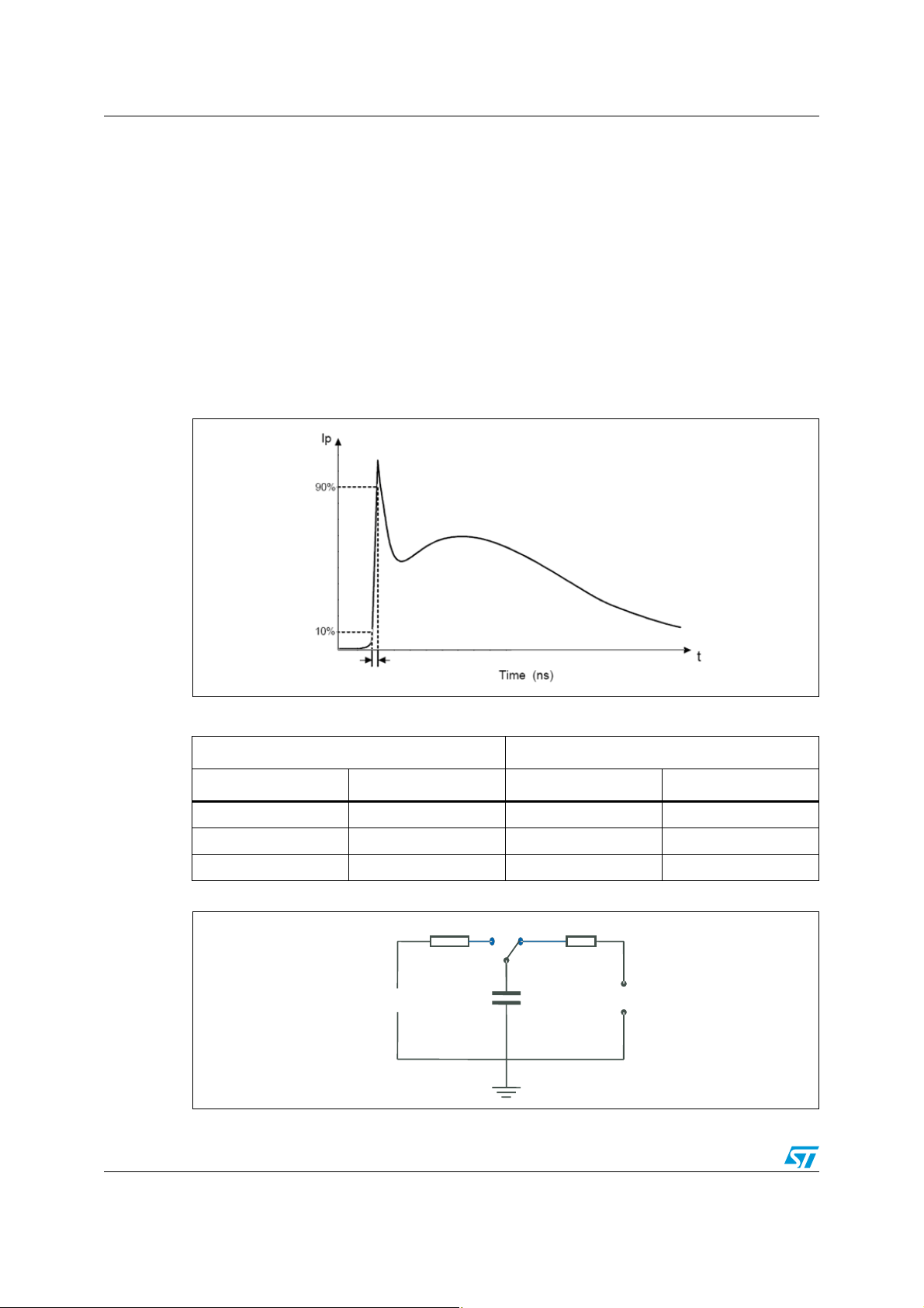
The ESD current waveform, shown in Figure 14, has the corresponding generator circuit
given in Figure 15 when the generator output is in short circuit.
This surge is specified for contact or air-discharge as shown in Ta bl e 1 and maximum
voltage occurring is a 25 KV (air-discharge)
Figure 14. ESD current waveform with generator output in short circuit
tr 1 ns≤
Table 1. Surge voltage levels for contact and air discharge
Contact discharge Air discharge
Level Test voltage (kV) Level Test voltage (kV)
1±4 1±8
2±62±15
3±83±25
Figure 15. Equivalent circuit schematic (occupant discharge model)
R (MΩ )2 kΩ
High voltage
supply
330 pf
Device
under test
12/41 Doc ID 14310 Rev 2
Page 13
AN2689 Data line protection
If we consider the +25 kV air discharge surge test, then, regarding the suggested
application given in Figure 16: the worked example below may be used as a guideline for
protection solution selection.
Figure 16. ISO 10605 ESD test set-up
Surge
Generator
Vs = 25 kV contact
= 2 kΩ
Rs
tr
≤
1 ns
Vcl
Module to protect
= 13.5 V
Vnom
Vmax
= 45 V
Tmax
= 85 °C
Identification of the best protection (Transil)
About the module to protect:
● The protection shall be “transparent” for the normal operating conditions of the module,
in this case 13.5 V.
● The maximum voltage the module can withstand is 45 V so the Transil will not offer a
higher voltage than 45 V when acting.
● The max temperature is 85 °C.
About the surge to suppress:
● The maximum voltage (V
● The surge time constant duration τ is 660 ns (R*C).
● The maximum repetition is one strike (t1).
● The internal series resistor of the generator is 2 kΩ.
About the Transil:
● The suppressor has the following electrical characteristics (Figure 17):
) of the surge is 25 kV.
pp
Figure 17. Transil diode electrical characteristics
I
Ipp
I
V
Irm
Vcl
Vrm
Vbr
If
Vf
V
Where:
V
is the stand-off voltage measured @Irm. This corresponds to the nominal voltage of the
rm
application V
≥ 13.5 V.
rm
Doc ID 14310 Rev 2 13/41
Page 14

Data line protection AN2689
Vbr is the breakdown voltage measured @1 mA. This corresponds to the beginning of the
action of the Transil.
V
is the clamping voltage Vcl ≤ 45 V. Its value depends on the current that flows through the
cl
device. The relationship between this parameter and the current is given by:
IppRdVbrVcl *+=
Where:
● R
● I
● I
● V
is the dynamic resistance of the Transil.
d
is the current imposed by the surge generator.
pp
is the leakage current measured @Vrm.
rm
is the direct voltage drop measured at current If depending on the application.
f
3.3 Design calculation example
Whatever the protection device package choice, the final choice will be directly linked to the
power dissipation demanded by the surge.
Power is:
IppVclPpp *=
with
IppRdVbrVcl *+=
The important missing parameter to solve these equations is the dynamic resistance R
which depends on the current value imposed by the surge.
3.3.1 Determination of R
Rd is the dynamic resistance of the Transil. It is dependent on the current surge rate and
duration.
R
is calculated by:
d
Rd
Where V
For example, considering an SM6T27A device (Figure 18), we can determine the R
pulse duration t
Figure 18. SM6T27A package
-
VbrVcl
=
cl
max
Ipp
is the dynamic clamping voltage measured at Ipp for exponential surge duration.
= 1 ms thanks to the 10/1000 µs parameters of Ta bl e 2 :
p
,
d
d
for a
d
A
K
Unidirectional
14/41 Doc ID 14310 Rev 2
Page 15

AN2689 Data line protection
Table 2. SM6T27A electrical characteristics, parameter values (T
V
IRM @ V
RM
VBR @ I
@ I
(1)
R
CL
10/1000 µs
PP
V
8/20 µs
CL
amb
@ I
= 25 °C)
PP
αT
(2)
C
Order code
max min. typ. max max max max typ.
µA
=25°C)µA(Tj=85°C)
(T
j
VVVVmAV AVA10
-4
/°C pF
SM6T27A 0.5 1 23.1 25.7 27 28.4 1 37.5 16 48.3 83 9.6 1150
1. Pulse test: tp < 50 ms.
2. ΔVBR = αT * (T
Rd
1000/10 µs
- 25) * VBR(25 °C).
amb
-
=57.0
4.285.37
16
Ω=
In the same way we can determine Rd for tp = 20 µs pulse duration. In this case we should
refer to the 8/20 µs parameters of Ta b le 2 .
-
=24.0
Rd
20/8µs
For other t
For t
p
pulse durations the next procedure should be considered:
p
< 20 µs, Rd is approximately equivalent to R
4.283.48
83
Ω=
so we consider the 8/20 µs
d20 µs
parameters of Ta bl e 2 .
For 20 µs < t
Rd
tp
For tp > 1 ms, R
=
α
< 1 ms, R
p
RdRd
-
201
980
is given by the following (tp is the pulse duration in s in this case):
dtp
⎛
⎜
1
-=
-
ajtp
⎜
⎝
is given by (tp in µs):
dtp
µsms
()
-
tp
τ
Rdtp
20
+-
20
Β
⎞
2
⎟
VbreTRthRd
nom
⎟
⎠
µs
αT is the temperature coefficient of V
R
is the thermal impedance of the device at the junction-ambient area.
thj-a
given in the Transil datasheet (see Tabl e 2 ).
br
τ, and Β define the transient thermal impedance. These parameters depend on the package
as shown in Ta bl e 3 .
Table 3. Transient thermal impedance versus packages
Package B τ(s) R
SMA 0.47 22 120
SMB 0.40 40 100
SMC 0.48 45 75
D2 PACK 0.63 120 60
Doc ID 14310 Rev 2 15/41
thj-a
(°C/W)
Page 16

Data line protection AN2689
µ
During an ESD strike, the voltage diagrams look like those given in Figure 19.
Figure 19. Voltage diagrams during an ESD strike
Vs
ESDwaveform
τ
= RC
Vcl
Voltage and
across the transil
current
Ip
Ip/2
3.3.2 Power dissipation determination
To make sure the power of the surge will not damage the Transil we need to determine the
power dissipated in the Transil.
Dissipated power is given by:
IppRdVbrVcl *+=
Ipp-=
and
In this study, the transient duration is much lower than 20 µs, therefore we consider R
equivalent to R
This R
Section 3.3.1: Determination of R
So
Rd
Rd
Then the power dissipation can be determined from:
VclVs
Rs
IppVclPpp *=
.
d20 µs
can be easily calculated thanks to the Transil datasheets (see example given in
d20µs
µs
20
20 µs
µs
=
Ipp
=0.24Ω
+=
VbrVcl
-
max20
s
20
IppRdVbrVcl
µs
20max
for SM6T27A)
d
t’ t
d
Ipp
Vbr
max
=
≈ Vbr
+
min
VbrVs
RdRs
+ 10%
20
max
µs
16/41 Doc ID 14310 Rev 2
Page 17

AN2689 Data line protection
Considering the ISO 10605 surge with Vpp = +25 kV, Rs = 2000 Ω and V
= 28.4 V, the
brmax
calculation produces:
VsRdRsVbr
+
µs
Vcl
=
Ipp
VbrVs
-
=
RdRs
+
20max
RdRs
+
µs
20
max
µs
20
Then Vcl = 31.4 V and Ipp = 12.5 A
Therefore the maximum residual voltage that will be applied to the module is lower than the
maximum voltage admissible (<45 V).
The question now is to determine if the Transil is able to withstand the power of the surge.
The peak pulse power (P
) dissipated in the Transil is:
pp
WPppIppVclPpp 392=⇒*=
To see if this power can be supported by the Transil, it is necessary to determine the
duration of the current that crosses the Transil during the surge compared to the peak pulse
power versus exponential pulse duration graph shown in Figure 20 (also in the datasheet).
Care must be taken at this step because the duration to be considered is the pulse duration
at I
/2. So it is necessary to determine the current surge duration (t’ in Figure 19) that
p
corresponds to half of the peak current crossing the Transil.
Figure 20. Peak pulse power versus exponential pulse duration
Doc ID 14310 Rev 2 17/41
Page 18

Data line protection AN2689
Figure 21. ESD ISO 10605 equivalent circuit
R (MΩ)
2 kΩ
Ic
High voltage
supply
Vc
330 pf
Considering the generator circuit sown in Figure 21, which respects the ESD surge
standard, the following equations apply:
tIc
)(
VbrtVc
-=)(
RdRs
+
And
tIc)()(-=
tCdVc
dt
Hence the equation
)()(
Vbr
t-CdVc
dt
tVc
=
-
RdRs
+
RdRs
+
(t) can also be expressed as:
V
c
λ
where λ is a coefficient and Y
tdVc=)(
dt
t
-
()
RdRsC
+
exp)(YtVc
-
λ
()
+=
0
a constant. Thus:
0
-
1
+
RdRsC
t
()
+
RdRsC
+
0exp
For the initial conditions the limit of Vc when t tends to 0 is given by:
t
-
VbrVc
-
0
RdRs
+
⎡
C
λ
-=
⎢
⎢
⎣
1
-
()
RdRsC
+
()
⎤
RdRsC
+
0exp
+
⎥
⎥
⎦
This reduces to
VbrVc
-
0
+
λ
=
RdRsRdRs
+
Then
()
VbrVc -=0λ
and thus
()
VbrYVbrVcVcY=⇒--=
0000
To determine the current, it is necessary to evaluate the voltage equation which is:
t
-
()
RdRsC
()
0
+
VbrVbrVctVc
exp)(
+-=
18/41 Doc ID 14310 Rev 2
Page 19

AN2689 Data line protection
It becomes then
t
-
()RdRsC
+
()
)(
--=exp
0
VbrVcCtIc
()
-1
RdRsC
+
then
t
VbrVc
-
0
tIc
=exp)(
RdRs
+
-
()RdRsC
+
So to determine the time duration (t’) at half value of the max current crossing the Transil,
use the equation:
t
-
exp
'
()
RdRsC
+
VbrVc
-
1
RdRs
+
2
VbrVc
-
00
=
RdRs
+
which reduces to
()
2ln'RdRsCt+=
This produces a duration of t’ = 457 ns.
If now we use this value in the peak pulse power versus exponential pulse duration graph in
Figure 20, we can see that the SM6T27A Transil is able to withstand more than 100 kW
power dissipation for a 457 ns pulse duration (extrapolation of Figure 20). As the application
can be submitted to an ambient temperature of +85 °C maximum, it is necessary to apply a
derating factor to this value. Figure 22 from the datasheet indicates the derating factor we
must apply.
Figure 22. Peak power dissipation versus initial junction temperature
%
100
80
60
40
20
Tj initial (° C)
0
0
20
40 60 80 100 120 140 160 180 200
Figure 22 shows that the derating factor is about 75% of the maximum power admissible.
Then the device will be able to withstand more than 75 kW for a 457 ns surge duration as
described in this example.
So compared to the application example where Ppp = 392 W, the SM6T27A device is more
than suitable for the application
The SM6T27A is too powerful with regards to the ISO 10605 test. Then, consider the use of
a less powerful device such as the ESDA25L shown in Figure 23.
Doc ID 14310 Rev 2 19/41
Page 20
Data line protection AN2689
Figure 23. Package and internal circuit of the ESDA25L
3
1
2
3
1
2
This device has the following characteristics:
Table 4. ESDA25L electrical characteristics
Order code
@ I
V
BR
R
min. max. max. max. typ.
VVmAµAVVmAmΩ 10
IRM @ V
RM
VF@ I
F
R
d
(1)
α
TC
(2)
max.
-4
/°C pF
ESDA25L 25 30 1 1 24 1.2 10 1000 10 50
1. Square pulse, Ipp = 15 A, tp = 2.5 µs.
2. Δ VBR = αT* (T
- 25 °C) * VBR (25 °C)
amb
Figure 24. Peak pulse power versus exponential time duration
P (W)
PP
3000
T initial = 25°C
j
typ.
0 V bias
1000
100
t (µs)
10
1 10 100
p
In the same way as for the SM6T27A, the calculations give:
R
= 1 Ω, Vcl = 42.5 V, Ipp = 12.5 A
d
then P
= 531 W
pp
and the t’ current pulse duration is still 457 ns.
Figure 24 shows that for 457 ns pulse duration the maximum power the ESDA25L can
dissipate is higher than 2 kW. The ambient temperature derating makes a maximum power
dissipation higher than 1.5 kW so the ESDA25L device would be suitable in this protection
application.
20/41 Doc ID 14310 Rev 2
Page 21

AN2689 Supply rail protection
4 Supply rail protection
4.1 Protection topology
4.1.1 Clamping topology
For supply rail protection the recommended topology is the “clamping topology”.
Figure 25 shows a schematic of the supply rail protection topology.
Figure 25. Supply rail protection using a Transil
Vbat
Transil
Module to protect
Vnom
Vmax
Accessory Connector
The choice of the protection device depends on the surge that is applied. To illustrate the
possible device selection, two protection examples are given below.
4.2 Supply rail protection example 1: pulse 2 ISO 7637-2
Pulse 2 from ISO 7637-2 standard corresponds to a surge, which is produced by a sudden
interruption of current in a device connected in parallel with the Transil, due to inductance in
the wiring harness. The pulse is directly applied to the battery and is a positive pulse. See
Figure 26 for the pulse characteristics.
The typical parameters are:
● Rise time (10-90%) - approximately 10 µs (t
● Pulse width (10-90%) - typically 50 µs (t
● Pulse amplitudes from +37 V to +50 V (V
● Pulse repetition from 0.2 Hz to 5 Hz (F)
● Output impedance 2 Ω
)
r
)
d
)
s
Doc ID 14310 Rev 2 21/41
Page 22
Supply rail protection AN2689
Figure 26. ISO 7637-2, pulse 2 waveform characteristics
t
1
t
d
t
r
0.9 Vs
V
s
0.1 Vs
V
a
0V
1/F
Figure 27. ISO 7637-2, pulse 2 test set up
Surge
Generator
Vs = 50 V
Ω
Rs = 2
td = 50 µs
Tr = 1 µs
F = 0.2 Hz to 5 Hz
Transil
Vcl
Module to protect
Vnom =13.5 V
Vmax = 45 V
Tmax = 85 °C
As for the examples in Section 3, it is necessary to check if the residual voltage after the
protection device is safe for the electronic module and if the protection device itself can
handle the power dissipated in the protection device during the suppression.
Let’s consider an SM15T33A protection device (Figure 28). Its specifications are given in
Ta bl e 5 and Ta bl e 6 .
Figure 28. SM15T33A package
A
K
Unidirectional
22/41 Doc ID 14310 Rev 2
Page 23

AN2689 Supply rail protection
Table 5. SM15T33A electrical characteristics (extract from datasheet)
V
@ I
CL
PP
Order
code
IRM @ V
max
RM
VBR @ I
(1)
R
10/1000 µs
min. typ. max max max
µA V V V V mA V A V A 10-4/°C pF
SM15T33A 1 28.2 31.4 33 34.7 1 45.7 33 59.0 169 9.8 2700
1. Pulse test: tp < 50 ms.
2. ΔVBR = αT * (T
3. VR = 0 V, F = 1 MHz.
Table 6. SM15T33A thermal parameter (extract from datasheet)
amb
- 25) * V
BR (25°C)
Symbol Parameter Value Unit
@ I
V
CL
8/20 µs
PP
αT
max
(2)
typ
C
(3)
R
th(j-a)
Junction to ambient on printed circuit on recommended pad layout 75 °C/W
4.3 Calculations for example 1
4.3.1 Determination of R
The voltage and current across the Transil are:
max
VbrVs
-
Ipp
=
Because Rd is dependent on the surge current duration and because its value for
ISO 7637-2 pulse 2 is not given in the datasheet, it is necessary to determine it to solve the
equations. But this time the generator internal schematic is not provided and none of the
internal elements are known. So the easiest way to determine the current duration is to refer
to the generator characteristics that are given in Figure 29 and Figure 30. These curves
were produced from a SCHAFFNER NSG5500, MT5510 module. The voltage curve is for
open circuit and the current curve produced when terminations were short circuited.
Figure 29. MT5510 output voltage in open circuit
max
RdRs
+
d
IppRdVbrVcl *+=
Test conditions
50 V, 50 µs
Rs = 2
Ω
0.2 s period
Doc ID 14310 Rev 2 23/41
Page 24

Supply rail protection AN2689
Figure 30. MT5510 output current in short circuit
Ipp = 23.5
t = 3.8 µs
At I = 0.5 Ipp, t = 0.7
then = 5.4 µs
τ
τ
In Figure 30 the current waveform shape corresponds to the pulse 2 of the ISO 7637-2
standard delivered by the SCHAFFNER NSG5500 generator when terminations are short
circuited.
As can be seen in Figure 30, the time constant is 5.4 µs duration when the generator
outputs are short circuited. When:
tIppi7.05.0=→= τ
therefore
8.3
7.0
µs4.5
=⇒= ττ
The current surge duration is below 20 µs. So, as explained previously when the duration is
below 20 µs, consider the R
VbrVcl
-
=
µs
= 0.14 Ω
20
Ipp
Rd
20
Rd
20 µs
nomµs
µs
20
to be the same as R
d<20µs
d20µs
From the equations in Section 4.3 on page 23, Vcl = 35.8 V and Ipp = 7.65 A, which means
the residual over voltage will be consistent with the admissible maximum voltage of the
module to protect.
4.3.2 Power dissipation determination
On the other hand the peak power dissipation in the Transil is:
WPppIppVclPpp 274*=⇒=
From the previous calculation in Section 3.3.2 on page 19, the current duration at I
will cross the Transil during the surge is given by the equation:
()
and the time constant is
RsC=τ
24/41 Doc ID 14310 Rev 2
2ln'RdRsCt+=
/2 that
p
Page 25

AN2689 Supply rail protection
where Rs is the serial resistor of the generator. In this case Rs = 2 Ω
So the surge generator capacitor is C =
SM15T33A, the current duration at I
6
-
µstp
()
+*=
2ln14.02107.2
tp
ATSM
3315
=
ATSM43315
2.7 µF. Therefore, when considering the use of an
/2 is:
p
(tp is the current duration through the SM15T33A measured between Ip and Ip/2)
It is now possible to compare this current duration with the curve given in Figure 31.
For a current duration of 4 µs, the peak pulse power the SM15T33A can dissipate is
approximately 20 kW.
Figure 31. Peak pulse power versus exponential pulse duration
P (kW)
PP
100.0
10.0
1.0
t (ms)
p
0.1
1.E-03 1.E-02 1.E-01 1.E+00 1.E+01
In the same way as for the previous examples, a derating factor needs to be considered
regarding the ambient temperature. For 85 °C ambient temperature the derating is close to
70% (see Figure 32). So the maximum peak power the SM15T33A can withstand for a 4 µs
is instead 14 kW.
Figure 32. Peak power dissipation versus initial junction temperature
%
00
80
60
40
20
T initial (°C)
0
0
20
40 60 80 100 120 140 160 180 200
j
Doc ID 14310 Rev 2 25/41
Page 26

Supply rail protection AN2689
4.3.3 Junction temperature determination
Another point to consider is the surge repetition. This would make the SM15T33A junction
temperature rise. It is necessary to make sure this junction temperature rise will not pass the
maximum specified. As per the SM15T datasheet, T
maximum ratings).
To clarify the situation, consider Figure 33 where current, voltage and junction temperature
rise are shown:
Figure 33. Voltage, current, and junction temperature behavior with surge repetition
Vs = 50 V
t = RC
Vcl = 36.5 V
Ip = 12.5 A
Ip/2
is specified as 150 °C (absolute
jmax
4µs
Tj
t0
1/F
For repeated surges it is necessary to determine the average power (P
t
) that the
av
SM15T33A will have to dissipate.
There is a relationship between the exponential surge duration curve and square shape
surge duration. Figure 34 illustrates the relationship between these types of surge.
Figure 34. Relationship between exponential pulse and square pulse duration
Ip
Ip/2
tp
tt
Ip
1.4tp
As shown on Figure 34, the current duration for equivalent square pulse duration is 1.4
times longer than the one measured at I
/2 for an exponential surge. So we have the
p
following equation:
6
tpIpp
4.1
*
2/
I
=
AV
Ip
T
=⇒
AV
-
1044.17.65
***
2.0
mAI
21.0
=
26/41 Doc ID 14310 Rev 2
Page 27

AN2689 Supply rail protection
Where tp is the current duration at Ip/2 and T the minimum surge period.
Then the average power is:
mWPVclIP
7.52=⇒*=
AVAVAV
The junction temperature can be calculated as:
RthPTambTj
+=
ajAV
-
with Rth
= 75 °C/W.
j-a
The junction temperature will rise by less than 1 °C over the maximum ambient temperature.
So the maximum junction temperature will not be exceeded. Therefore the SM15T33A will
be suitable for the application.
In the meantime, comparing the 274 W power induced by the surge with the SM15T33A
admissible power, the SM15T33A is extremely safe regarding the ISO 7637-2 pulse 2 surge,
even over-specified.
For this reason it would be more effective to choose a smaller Transil, like, for instance, an
SMAJ30A (V
= 33.3 V). The same calculations show the power dissipation is quite
brmin
similar to the SM15T33A results. Figure 35 and Figure 36 show that the maximum power
this SMAJ30A can dissipate for 4 µs exponential pulse duration is still higher than that the
surge imposes. The SMAJ30A is able to withstand more than 3 kW for 4 µs surge duration.
Figure 35. Peak pulse power versus exponential time duration of an SMAJ Transil
PPP(kW)
10.0
1.0
Tjinitial = 25 °C
0.1
1.0E-03 1.0E-02 1.0E-01 1.0E+00 1.0E+01
tP(ms)
Figure 36. Peak power dissipation versus initial junction temperature of SMAJ
Transil
%
110
100
90
80
70
60
50
40
30
20
10
0
0 25 50 75 100 125 150 175 200
Doc ID 14310 Rev 2 27/41
Tj(°C)
Page 28

Supply rail protection AN2689
4.4 Supply rail protection example 2: pulse 5a load dump ISO 7637-2
The load dump is caused by the discharged battery being disconnected from the alternator
while the alternator is generating charging current
Parameters are:
● Pulse width -t
● Pulse amplitude -V
● Impedance is R
● V
= 13.5 V
bat
Figure 37. ISO 7637-2, pulse 5a waveform characteristics
[40 to 400 ms]
d
[65 to 87 V]
s
[0.5 Ω to 4 Ω]
s
0.9Vs
t
d
t
r
V
s
V
0V
bat
0.1Vs
t
Figure 38. Load dump protection test set up
Surge
Generator
Vs = 87 V
Rs=2Ω
td = 100 ms
Tr = 10 ms
Vbat = 13.5 V
Transil
Vcl
Module to protect
Vnom =13.5 V
Vmax =45 V
Tmax = 85 °C
In the same manner as for the last case (ISO pulse 2), we have to determine if the residual
voltage after the protection device is safe for the electronic module and if the power
dissipation involved in the protection device during the suppression is supported by the
protection device itself.
Consider now the RBO40-40 device (see Figure 39) which offers a surge protection
capability and a reverse battery protection.
28/41 Doc ID 14310 Rev 2
Page 29

AN2689 Supply rail protection
Figure 39. Package and internal schematic of the RBO40-40
1
D2PAK
RBO40-40G
3
2
Its specifications are the following:
Table 7. RBO40-40G electrical characteristics, Transil T2 (-40 °C < T
Symbol Test conditions Min. Typ. Max. Unit
V
BR 32
V
BR 32IR
I
RM 32
I
RM 32
V
CL 32IPP
αT Temperature coefficient of V
C
1. One pulse
IR = 1 mA 22 35 V
= 1 mA, T
= 25°C 24 32 V
amb
VRM = 20 V 100 µA
VRM = 20 V, T
= 20 A
F = 1MHz VR = 0 V 8000 pF
32
= 25°C 10 µA
amb
(1)
tp = 10/1000µs 40 V
BR
< +85 °C)
amb
910-4/°C
4.5 Calculations for example 2
The voltage and current across the Transil are:
max
-
Ipp
=
+
As with the previous example, the internal elements of the surge generator are not known.
So, the easiest way to proceed is to refer to the voltage and current curves of the generator.
With voltage and current curves produced from a SCHAFFNER NSG5500, LD5505 module,
(see Figure 40 and Figure 41), we can measure the duration t
duration between I
IppRdVbrVcl *+=
VbrVs
RdRs
and Ip/2
p
which corresponds to the
p
Doc ID 14310 Rev 2 29/41
Page 30

Supply rail protection AN2689
Figure 40. LD5505 output voltage in open circuit
Test conditions
87 V, 100 ms
13.5 V battery voltage
Rs = 2 Ω
Figure 41. LD5505 output current in short circuit
Ipp = 40 A
At I = 0.5 Ipp, tp = 0.7
so = 40.7 ms
τ
τ
Figure 41 shows the current waveform corresponding to the pulse 5a of the ISO 7637-2
standard delivered by the SCHAFFNER NSG5500 generator when terminations are short
cicuited.
The t
duration measured between Ip and Ip/2 is 28.5 ms. Then the time constant calculated
p
is 40.7 ms (generator outputs short circuited).
4.5.1 Determination of R
For tp > 1 ms, R
α
is in seconds in this case.
t
p
τ, and Β define the transient thermal impedance (see Table 3: Transient thermal impedance
versus packages).
When the surge is applied to the RBO40-40 transient suppressor:
4040 tpRBO
-
is given by:
dtp
-
⎛
⎜
1
-=
ajtp
-
⎜
⎝
()
RdRsCtp +=
tp = 28.5 ms
d
Β
tp
⎞
τ
⎟
⎟
⎠
2
VbreTRthRd
nom
2ln
And the time constant is
τ = R
s
C.
30/41 Doc ID 14310 Rev 2
Page 31

AN2689 Supply rail protection
So, C = 20.35 mF.
Hence:
3
-
4040
-
RBO
-
4
*
*
tp
()
tp
-
⎛
120
⎜
eRd
-=
⎜
⎝
2ln21035.20
Rdtp +*=
63.0
⎞
⎟
⎟
⎠
2
35160109
nom
Then, thanks to the test curves from the load dump generator, the result is tp = 33.6 ms and
R
= 0.36 Ω.
d
From the equations in Section 4.5 on page 29, V
= 41.2 V and Ipp = 16.25 A, which means
cl
the residual over voltage will be consistent with the admissible maximum voltage of the
module to protect.
4.5.2 Power dissipation determination
The peak power dissipation in the Transil will be:
WPppIppVclPpp 670=⇒*=
Figure 42, shows that for 33.6 ms exponential surge duration the maximum admissible
power the RBO40-40 can withstand is approximately 900 W.
Figure 42. Peak pulse versus exponential surge duration
Ppp(kW)
10.0
5.0
2.0
Tra ns il T2
1.0
0.5
0.2
0.1
1
2 5 10 20 50 100
Tra ns il T1
tp(ms)
Figure 43. shows the derating factor for the ambient temperature effect.
Figure 43. Relative variation of peak power versus junction temperature
Ppp[Tj]/Ppp[Tj initial=85°C]
1.20
1.00
0.80
0.60
0.40
0.20
0.00
Tj initial (°C)
25 50 75 100 125 150 175
0
Doc ID 14310 Rev 2 31/41
Page 32

Supply rail protection AN2689
For +85 °C ambient temperature, the derating factor is 1. So the power dissipation induced
by the load dump surge is supported by the RBO40-40 device.
The RBO40-40 combines a transient suppressor diode and also a reverse battery
protection. This function is helpful in case of battery polarity inversion that can occur by
mistake. A direct diode is placed in series with the power supply so that all power supply
inversion is safe for the protection diode (see Figure 43).
The direct diode reverse battery protection can also be replaced with a simple fuse.
However, upon battery inversion this fuse will blow and the module will need to be replaced
or repaired.
Figure 44. Use of serial protection devices for reverse battery prevention
Reverse
battery
fuse or diode
protection
or
Transil
Module to protect
Besides the ISO pulse 2a the Transil has to eliminate, and the reverse battery protection,
there is another condition to consider in the automotive environment. This condition is the
starting aid.
The starting aid covers the possibility of starting 12 V vehicles with a 24 V truck battery in
case of emergency. Then, the Transil nominal voltage will need to be higher than this
starting aid voltage. That is the reason the Transil nominal breakdown voltage is 27 V
minimum. In this case the Transil is not active during starting aid test. No dissipation occurs
in the device so the Transil is safe.
32/41 Doc ID 14310 Rev 2
Page 33

AN2689 PCB layout recommendations
5 PCB layout recommendations
Once the protection device has been selected, the designer has to pay attention to the
device placement on the board. This is because the device placement has a big impact on
protection efficiency and on parasitic electromagnetic coupling.
5.1 Parasitic inductances of the Transil and the PCB tracks
5.1.1 Parasitic inductance from Transil wiring
Figure 45 provides an example of a protection schematic.
Figure 45. Protection circuit schematic using a Transil
Sensitive line
Accessory Connector
Transil
Module to protect
Vnom
Vmax
Figure 46. shows what happens in the circuit when an over voltage occurs on the sensitive
protected line. The over voltage surge is suppressed by the Transil. When the voltage
reaches the breakdown voltage of the Transil, a current I crosses the protection device and a
residual voltage V is applied at the module input line.
Figure 46. Current and voltage at the Transil termination when a surge is applied
Vs
Module to protect
Sensitive line
I
Accessory Connector
Transil
V
Vnom
Vmax
This is the simple representation of the Transil action but in fact things are more complicated
and the more realistic circuit is given in Figure 47.
Doc ID 14310 Rev 2 33/41
Page 34

PCB layout recommendations AN2689
Figure 47. Parasitic elements due to the wiring
Parasitic elements
Vs
Module to protect
Vnom
I
Accessory Connector
Transil
V1
Vcl
V2
V=V1+Vcl+V2
Vmax
Figure 47 shows there are two major parasitic elements:
● Some parasitic inductance each side of the Transil
● Some parasitic capacitance between lines
There is also some parasitic inductance brought by the lines themselves. These parasitic
elements cause inductive and capacitive coupling.
These parasitic couplings may induce over voltages or electromagnetic noise on adjacent
lines which have nothing to do with the protected lines.
The parasitic inductance is directly due to the PCB routing. The wiring tracks to the
protection device may drastically affect the efficiency of the protection device.
Consider a 35 µm copper track, 0.3 mm wide (W), spaced at 0.5 mm (h) from a ground
plane (see Figure 48). This gives the ratio h/W of 1.7. Figure 49 (AEMC source) shows, for
an h/W ratio of 1.7, a parasitic inductance of 5 nH/cm.
Figure 48. Double sided PCB structure - single track
w
εr=4.5
Figure 49. Inductance variation versus PCB thickness for single copper track
(AEMC source)
L (µH/m) versus h/W
1
L(µH/m)
h
0.1
0.1 1 10
34/41 Doc ID 14310 Rev 2
h/w
Page 35

AN2689 PCB layout recommendations
Consider the PCB layout example in Figure 50. The lengths of track that connect the Transil
to the sensitive line and the ground line are respectively 10 mm and 6 mm.
These lines show inductances of approximately 5 nH and 3 nH as shown in the schematic in
Figure 51
Figure 50. PCB routing example
10 mm long
TVS in
SMA package
6 mm long
Module to protect
Vnom
Vmax
Figure 51. Parasitic inductance due to the wiring tracks
≈
H 5 nH
≈
H 3 nH
When a +25 kV ESD air discharge is applied (ISO 10605) the remaining voltage at the
module to protect is split in three parts as shown in Figure 52.
Figure 52. Parasitic inductance effect on fast transient
+25kV ESD ISO10605
L1di/dt
Module to protect
Vnom
Vmax
The Transil offers a clamping voltage V
Vcl
L2di/dt
and an internal resistance “Rd”. Whereas the
cl
V=L1di/dt+Vcl+L2di/dt
inductors bring on over voltage Ldi/dt.
To determine the Ldi/dt voltage
The ESD surge generator has an internal resistor of 2 kΩ. The max Voltage is +25 kV, the
rise time of the surge is specified as t
The current that would cross the Transil is:
Vcl
25000≈≈-
I5.12
=
2000
25000
2000
A
Doc ID 14310 Rev 2 35/41
≤ 1ns
r
Page 36

PCB layout recommendations AN2689
Then
5.12
di
9
-
dt
10
105.12
19
-
**⇒=sA
Therefore, for L1, the over voltage is
di
L5.621 ≈
dt
V
and for L2 the over voltage is
di
L5.372 ≈
dt
V
That means the total over voltage seen by the module would be something close to V
+
cl
100 V! This shows that whatever the protection device, if the routing is not optimized there
will be a big impact of the track inductance to the protection device on the remaining voltage
in case of fast transient discharge. Figure 53. illustrates the recommended Transil wiring to
prevent this phenomenon.
Figure 53. Recommended Transil wiring
Transil in
SMA package
Module to protect
Vnom
Vmax
The equivalent schematic diagram for the recommended wiring layout is shown in Figure 54.
Figure 54. Details of the remaining voltage at the module to protect
+25kV ESD ISO10605
L1di/dt
I
L2di/dt
L1=L3 & L2=L4
In this layout the remaining voltage at the module to protect is:,
dI
dI
LVclV
3--=
dt
'
'
L
4
dt
So, in the worst case (when L3 = L4 = 0), V is equal to Vcl.
36/41 Doc ID 14310 Rev 2
L3di’/dt
Vcl
L4di’/dt
I’
Module to protect
Vnom
Vmax
V=Vcl -L3di’/dt-L4di’/dt
Page 37

AN2689 PCB layout recommendations
5.1.2 Capacitive and inductive coupling
The parasitic capacitance (see Figure 47) is due to the geometrical conception of the PCB
and the routing together. Figure 55 shows the effective capacitive coupling during surge
suppression.
Figure 55. Capacitive coupling representation
C
V
Vsurge
This parasitic capacitance depends on the PCB and track structures as shown in Figure 56
and Figure 57. This parasitic capacitance is defined by the space between tracks, the track
width and the PCB thickness as well.
Figure 56. Double side PCB structure in coplanar
d
w
εr=4.5
Figure 57. Track to track capacitance for double side PCB (source AEMC)
Capacitance (pF/cm)
1
0.3
0.1
0.03
0.01
0.003
d/h
0.001
0.1 0.3 1 3 10 30
h
h / w = 0.3
h / w = 0.5
h / w = 1
h / w = 2
h / w = 5
h / w = 10
The longer is the line to the protection device, the higher will be the capacitive coupling.
Doc ID 14310 Rev 2 37/41
Page 38

PCB layout recommendations AN2689
Inductive coupling is also present on the PCB. This is sometime also called “inductive crosstalk”. When over voltage occurs, a current crosses the track and makes this track radiate.
This coupling depends on the current variation rate (di/dt). The parasitic inductance coupling
is shown in Figure 58.
Figure 58. Inductive coupling representation
Isurge
Vsurge
I
Like capacitive coupling, the longer the tracks to the protection device the larger will be the
electromagnetic field.
The solution to minimize the capacitive and inductive coupling consists of placing the
protection device as close as possible to the accessories connector, where the surge impact
is the most probable. (Figure 59)
Figure 59. Where to place the protection device
Vs
Module to protect
Vnom
Transil
Accessory Connector
V
Vmax
38/41 Doc ID 14310 Rev 2
Page 39

AN2689 PCB layout recommendations
5.1.3 Parasitic coupling due to the loop-effect
In the presence of electromagnetic fields, caused by relay arcing or antenna emissions for
example, a loop coupling effect may occur as shown in Figure 60 (red dashed line)
Figure 60. Loop effect representation
Module to protect
Vnom
Transil
V
I
Accessory Connector
Hazard
source
This coupling is dependent on the loop size and the source distance (see Figure 61).
Figure 61. Electromagnetic field applied to a loop
Vmax
E,H
h
U
L
The loop effect voltage U is given by
2
U++=
λ
πhLLhE
[]
()
[]
()
4141
λλ
22
Where H is the magnetic field, E the electric field and λ the wavelength.
U is in Volts, L, h and λ are in metres and E in Volt/metre.
The lower the L and h values, the smaller would be the voltage U. That means the smaller
would be the parasitic coupling. So the solution is to minimize the track loop between the
protection device and the module as shown in Figure 62.
Figure 62. Loop optimization
Connector
Transil
Accessory
Big loop Smallloop
Module to protect
Vnom
Vmax
Connector
Transil
A ccesso ry
Module to protect
Vnom
Vmax
Doc ID 14310 Rev 2 39/41
Page 40

Conclusion AN2689
Figure 63 shows a recommended PCB layout using a protection device close to the
accessories connector, and with the track loop to the module to protect minimized.
Figure 63. Placement and routing of a protection device
6 Conclusion
Because the automotive environment is a major source of electrical hazards and electronic
equipment is becoming more sensitive, caution must be taken when electronic modules are
designed.
It is therefore very common to use protection devices to ensure the modules and systems
are safe from all hazards generated inside the vehicle.
The choice of the protection device is not easy, and moreover, surges are not well defined
even by the standards. This document helps the electronic module designer in the selection
of the protection device.
Calculations are sometimes good enough to dimension the protection device but in some
cases the surges in practice have to be monitored to determine the best protection.
Transil
Accessory connector
Module to protect
Vnom
Vmax
Some worked examples are given in this document, particularly for the IEC 10605 and ISO
7637-2, pulse 2 and pulse 5a. Thus the way these cases are treated offers the designer a
starting point for other kinds of surge, which are yet to be defined.
Beyond the guidance offered for choosing protection devices on the basis of standard
surges, other advice is given at the same time such as the protection device routing on PCB,
the PCB layout optimization, and the protection device placement.
As a result this document should be helpful in all automotive protection design approaches.
7 Revision history
Table 8. Document revision history
Date Revision Changes
21-Feb-2008 1 Initial release.
30-Mar-2010 2 Updated Figure 3 to include IEC 61000 references.
40/41 Doc ID 14310 Rev 2
Page 41

AN2689
Please Read Carefully:
Information in this document is provided solely in connection with ST products. STMicroelectronics NV and its subsidiaries (“ST”) reserve the
right to make changes, corrections, modifications or improvements, to this document, and the products and services described herein at any
time, without notice.
All ST products are sold pursuant to ST’s terms and conditions of sale.
Purchasers are solely responsible for the choice, selection and use of the ST products and services described herein, and ST assumes no
liability whatsoever relating to the choice, selection or use of the ST products and services described herein.
No license, express or implied, by estoppel or otherwise, to any intellectual property rights is granted under this document. If any part of this
document refers to any third party products or services it shall not be deemed a license grant by ST for the use of such third party products
or services, or any intellectual property contained therein or considered as a warranty covering the use in any manner whatsoever of such
third party products or services or any intellectual property contained therein.
UNLESS OTHERWISE SET FORTH IN ST’S TERMS AND CONDITIONS OF SALE ST DISCLAIMS ANY EXPRESS OR IMPLIED
WARRANTY WITH RESPECT TO THE USE AND/OR SALE OF ST PRODUCTS INCLUDING WITHOUT LIMITATION IMPLIED
WARRANTIES OF MERCHANTABILITY, FITNESS FOR A PARTICULAR PURPOSE (AND THEIR EQUIVALENTS UNDER THE LAWS
OF ANY JURISDICTION), OR INFRINGEMENT OF ANY PATENT, COPYRIGHT OR OTHER INTELLECTUAL PROPERTY RIGHT.
UNLESS EXPRESSLY APPROVED IN WRITING BY AN AUTHORIZED ST REPRESENTATIVE, ST PRODUCTS ARE NOT
RECOMMENDED, AUTHORIZED OR WARRANTED FOR USE IN MILITARY, AIR CRAFT, SPACE, LIFE SAVING, OR LIFE SUSTAINING
APPLICATIONS, NOR IN PRODUCTS OR SYSTEMS WHERE FAILURE OR MALFUNCTION MAY RESULT IN PERSONAL INJURY,
DEATH, OR SEVERE PROPERTY OR ENVIRONMENTAL DAMAGE. ST PRODUCTS WHICH ARE NOT SPECIFIED AS "AUTOMOTIVE
GRADE" MAY ONLY BE USED IN AUTOMOTIVE APPLICATIONS AT USER’S OWN RISK.
Resale of ST products with provisions different from the statements and/or technical features set forth in this document shall immediately void
any warranty granted by ST for the ST product or service described herein and shall not create or extend in any manner whatsoever, any
liability of ST.
ST and the ST logo are trademarks or registered trademarks of ST in various countries.
Information in this document supersedes and replaces all information previously supplied.
The ST logo is a registered trademark of STMicroelectronics. All other names are the property of their respective owners.
© 2010 STMicroelectronics - All rights reserved
STMicroelectronics group of companies
Australia - Belgium - Brazil - Canada - China - Czech Republic - Finland - France - Germany - Hong Kong - India - Israel - Italy - Japan -
Malaysia - Malta - Morocco - Philippines - Singapore - Spain - Sweden - Switzerland - United Kingdom - United States of America
www.st.com
Doc ID 14310 Rev 2 41/41
 Loading...