

Page 1

AN2687
Application note
STM8S20xxx
LCD software driver
Introduction
This application note describes two different methods for driving liquid crystal displays
(LCD) with any standard STM8S20xxx microcontroller (MCU), without any specific on-chip
LCD driver hardware:
● the first method uses the timer 2 channel resource and also allows LCD contrast
control through software
● the second method uses the Auto-wakeup mode only
This application note starts with an introduction on LCDs in Section 1: LCD principle and
Section 2: LCD drive signals.
Section 3 then presents a solution based on a standard STM8S20xxx MCU directly driving a
quadruplex LCD. This solution can be implemented with any MCU as it only requires the
standard I/O ports and some timings.
Section 4 gives consumption considerations. Section 5 describes how to control contrast
through software: for this purpose, two push-buttons connected to two standard I/Os are
used. Finally, Section 6 gives an overview of the LCD demo board based on an
STM8S20xxx microcontroller, and provides the board schematics.
For more information on the LCD drive theory, please refer also to AN1048.
The number of external components is kept to a minimum of two external resistors per COM
line. The number of I/Os depends on the number of LCD segments used. Software contrast
control is a very flexible solution that can be easily adapted to a wide range of applications.
April 2009 Doc ID 14296 Rev 1 1/22
Page 2

Contents AN2687
Contents
1 LCD principle . . . . . . . . . . . . . . . . . . . . . . . . . . . . . . . . . . . . . . . . . . . . . . . 5
2 LCD drive signals . . . . . . . . . . . . . . . . . . . . . . . . . . . . . . . . . . . . . . . . . . . 7
2.1 Quadruplex LCD drive . . . . . . . . . . . . . . . . . . . . . . . . . . . . . . . . . . . . . . . . 7
2.1.1 LCD mean voltage calculation . . . . . . . . . . . . . . . . . . . . . . . . . . . . . . . . . 8
2.1.2 Contrast calculation . . . . . . . . . . . . . . . . . . . . . . . . . . . . . . . . . . . . . . . . . 9
3 Example of a quadruplex LCD driver with STM8 . . . . . . . . . . . . . . . . . 10
3.1 First method: Timer 2 . . . . . . . . . . . . . . . . . . . . . . . . . . . . . . . . . . . . . . . . 12
3.2 Second method: Auto-wakeup . . . . . . . . . . . . . . . . . . . . . . . . . . . . . . . . . 13
4 Consumption considerations . . . . . . . . . . . . . . . . . . . . . . . . . . . . . . . . . 14
5 Software contrast control with the first method . . . . . . . . . . . . . . . . . 17
5.1 Contrast calculations . . . . . . . . . . . . . . . . . . . . . . . . . . . . . . . . . . . . . . . . 17
6 LCD demo board . . . . . . . . . . . . . . . . . . . . . . . . . . . . . . . . . . . . . . . . . . . 19
6.1 Board information . . . . . . . . . . . . . . . . . . . . . . . . . . . . . . . . . . . . . . . . . . . 20
7 Revision history . . . . . . . . . . . . . . . . . . . . . . . . . . . . . . . . . . . . . . . . . . . 21
2/22 Doc ID 14296 Rev 1
Page 3

AN2687 List of tables
List of tables
Table 1. LCD RAM . . . . . . . . . . . . . . . . . . . . . . . . . . . . . . . . . . . . . . . . . . . . . . . . . . . . . . . . . . . . . . 11
Table 2. First method - consumption (Timer 2) . . . . . . . . . . . . . . . . . . . . . . . . . . . . . . . . . . . . . . . . . 14
Table 3. Second method - consumption (AWU) . . . . . . . . . . . . . . . . . . . . . . . . . . . . . . . . . . . . . . . . 14
Table 4. Document revision history . . . . . . . . . . . . . . . . . . . . . . . . . . . . . . . . . . . . . . . . . . . . . . . . . 21
Doc ID 14296 Rev 1 3/22
Page 4

List of figures AN2687
List of figures
Figure 1. LCD principle . . . . . . . . . . . . . . . . . . . . . . . . . . . . . . . . . . . . . . . . . . . . . . . . . . . . . . . . . . . . 5
Figure 2. Equivalent electrical schematic of an LCD segment. . . . . . . . . . . . . . . . . . . . . . . . . . . . . . . 6
Figure 3. Basic LCD segment connection in quadruplexed mode . . . . . . . . . . . . . . . . . . . . . . . . . . . . 7
Figure 4. LCD timing diagram for quadruplex mode . . . . . . . . . . . . . . . . . . . . . . . . . . . . . . . . . . . . . . 8
Figure 5. Hardware connection diagram . . . . . . . . . . . . . . . . . . . . . . . . . . . . . . . . . . . . . . . . . . . . . . 12
Figure 6. LCD timing diagram with dead & active time (to decrease Vrms). . . . . . . . . . . . . . . . . . . . 15
Figure 7. LCD timing diagram with active and dead time (to increase Vrms) . . . . . . . . . . . . . . . . . . 16
Figure 8. Schematic diagram . . . . . . . . . . . . . . . . . . . . . . . . . . . . . . . . . . . . . . . . . . . . . . . . . . . . . . . 19
4/22 Doc ID 14296 Rev 1
Page 5
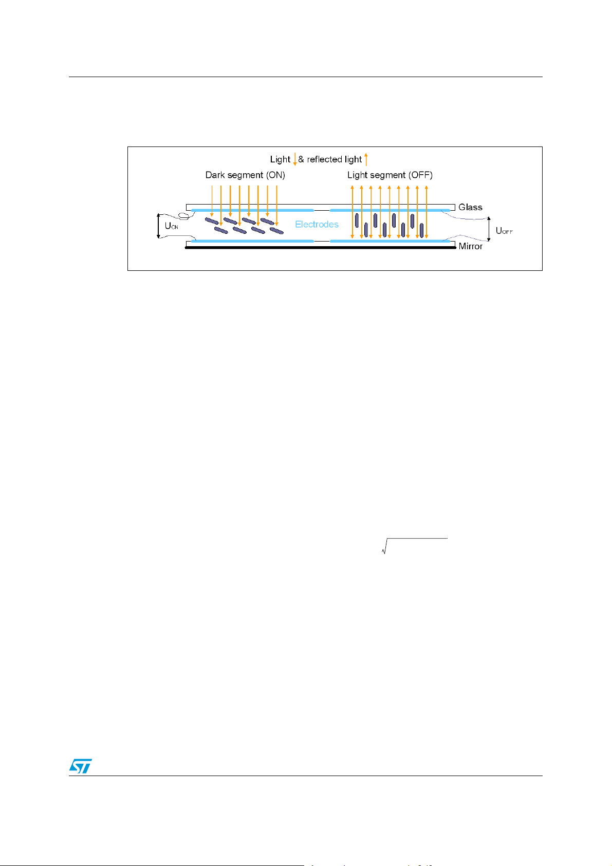
AN2687 LCD principle
Mean Signal
2
1 LCD principle
Figure 1. LCD principle
An LCD panel is composed of many layers. A liquid crystal is filled between two of them
(glass plates), which are separated by thin spacers coated with transparent electrodes that
contain orientation layers. The orientation layer usually consists of a polymer (e.g.
polyimide) which has been unidirectionally rubbed using, for instance, a soft tissue. As a
result, the liquid crystal molecules are fixed with their alignment more or less parallel to the
plates, in the direction of rubbing. The crystal alignment directions at the surface of the two
plates are perpendicular so that the molecules between the two plates undergo a
homogeneous twist deformation in alignment to form a helix.
If no electric field is applied, the birefringent liquid crystal molecules keep their helical
structure and rotate linearly polarized light waves passing through the plates. The
transmitted light wave is then allowed through a crossed exit polarizer. As a result, the
modulator has a bright appearance.
On the other hand, if an AC voltage of a few volts is applied, the resulting electric field forces
the liquid crystal molecules to align themselves along the field direction and the twist
deformation (the helix) is unwound. In this case, the polarization of the incident light is not
rotated by the crystal molecules and the crossed exit polarizer blocks the light wave. As a
result, the modulator appears dark.
The inverse switching behavior can be obtained with parallel polarizers. It must also be
noted that gray scale modulation is easily achieved by varying the voltage between the
crystal molecule reorientation threshold (reorientation is resisted by the elastic properties of
liquid crystals) and the saturation field.
LCDs are sensitive to root mean square voltage (Vrms= ) levels. With a low
root mean square voltage applied to it, an LCD is practically transparent (the LCD segment
is then inactive or off). To turn an LCD segment on, causing the segment to turn dark (from
light gray to opaque black), an LCD RMS voltage greater than the LCD threshold voltage is
applied to the LCD. The LCD RMS voltage is the RMS voltage across the capacitor C in
Figure 2, which is equal to the potential difference between the SEG and COM values.
The LCD threshold voltage depends on the quality of the liquid used in the LCD and the
temperature. The optical contrast is defined by the difference in transparency of an LCD
segment that is on (dark) and an LCD segment that is off (transparent). The optical contrast
depends on the difference between the RMS voltage on an on segment (V
voltage on an off segment (V
V
(rms), the higher the optical contrast. The optical contrast also depends on the level of
OFF
V
versus the LCD threshold voltage. If VON is below or close to the threshold voltage, the
ON
LCD is completely or almost transparent. If V
). The higher the difference between VON(rms) and
OFF
is close or above the threshold voltage, the
OFF
) and the RMS
ON
LCD is completely black.
Doc ID 14296 Rev 1 5/22
Page 6
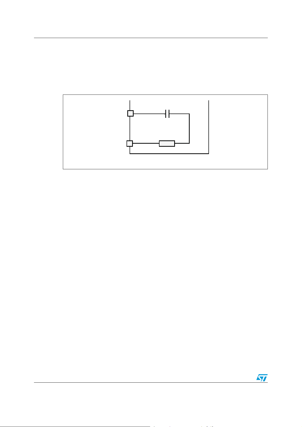
LCD principle AN2687
C
R
S
S
COM
ai14758
In this document, contrast is defined as D = VON(rms) / V
OFF
(rms).
The applied LCD voltage must also alternate to give a zero DC value to prevent the
electrolytic process and so, ensure a long LCD lifetime.
The higher the multiplexing rates, the lower the contrast. The signal period also has to be
short enough to avoid visible flickering on the display.
Figure 2. Equivalent electrical schematic of an LCD segment
Note: The DC value should never be more than 100 mV (refer to the LCD manufacturer’s
datasheet), otherwise the LCD lifetime may be shortened. The frequency range is 30 Hz to
200 Hz typically. If a lower frequency is used, the LCD flickers, if a larger frequency is used,
power consumption increases.
6/22 Doc ID 14296 Rev 1
Page 7
AN2687 LCD drive signals
S11
S1
COM1
ai14762
S2 S3
COM2
S14
COM3
COM4
S12
S13
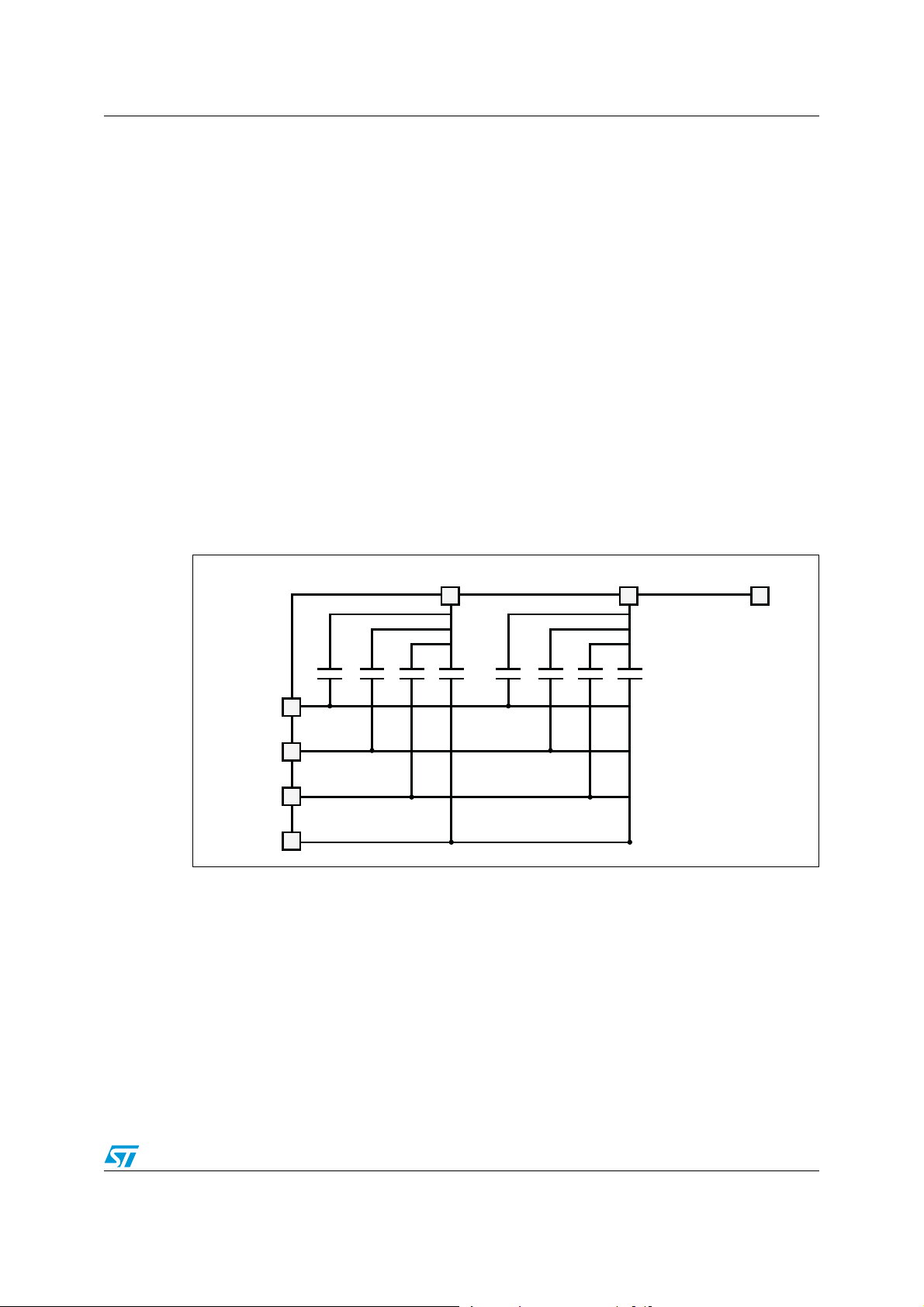
2 LCD drive signals
2.1 Quadruplex LCD drive
In a quadruplex LCD drive, four backplanes (common lines) are used. Each LCD pin is
connected to four LCD segments, whose other side is connected to one of the four
backplanes (refer to Figure 3). Thus, only (S/4)+4 MCU pins are necessary to drive an LCD
with S segments. For example, to drive an LCD with 128 segments (32 × 4), only 36 I/O
ports are required (32 I/O ports to drive the segments, 4 I/O ports to drive the backplanes).
Three different voltage levels have to be generated on the common lines: 0, V
The Segment line voltage levels are 0 and V
only. The LCD segment is inactive if the
DD
/2, VDD.
DD
RMS voltage is below the LCD threshold voltage and is active if the LCD RMS voltage is
above the threshold.
The intermediate voltage V
selected as backplanes are set by software to output mode for 0 or V
high-impedance input mode for V
/2 is only required for backplane voltages. The MCU I/O pins
DD
/2. The VDD/2 voltage is determined by two resistors of
DD
levels and to the
DD
equal value, externally connected to the I/O pins as shown in Figure 5. When one backplane
or COM is active, the other ones are neutralized by applying V
/2 to them.
DD
Figure 3. Basic LCD segment connection in quadruplexed mode
Doc ID 14296 Rev 1 7/22
Page 8

LCD drive signals AN2687
Figure 4. LCD timing diagram for quadruplex mode
COM1
COM2
COM3
COM4
Vsegx
V
COM
+VDD/2
Single-frame period
Control
period
T/8 T/4 T/2 3T/4 T
Segx_1 On Segx_2 Off Segx_3 On Segx_4 Off
LCD
COM1
COM2
COM3
COM4
SEG1
Vseg – V
COM
Vseg – V
COM1
2.1.1 LCD mean voltage calculation
The LCD mean voltage must be very close to zero to guarantee long life to the LCD. The
LCD mean voltage for On and Off periods can be calculated as shown below:
Vmean(On) = 1/8 Vseg + 1/8 (–V
Vmean(Off) = 3(Vseg/2) + 3(–Vr/2) (2)
Vmean(On) and Vmean(Off) assume identical periods for each phase.
Equating equations (1) & (2) to zero, that is putting Vmean(On) = 0 and Vmean(Off) = 0,
gives:
Vseg = V
● V
● Vr/2 is the voltage in the middle of the resistor bridge, applied on the COM line
● Vseg is the maximum voltage on the Segx line
● V
is the maximum voltage on the COM line
COM
is the microcontroller power supply
DD
= Vr = VDD, where:
COM
Vseg – V
) + 3(Vseg – Vr/2) + 3(–Vr/2) (1)
COM
COM4
ai15954
8/22 Doc ID 14296 Rev 1
Page 9

AN2687 LCD drive signals
1
T
---
ft2dt
0
T
1
T
---
VDD2dt VDD2dt
V
DD
2
----------
2
dt
2T
8
------ -
T
+
T
8
---
2T
8
------ -
+
0
T
8
---
1
T
---
VDD
2
T
8
--- VDD
2
T
8
---
VDD
2
4
------------------
6T
8
----------- -
++
0.661V
DD
=
1
T
---
0dt 0dt
V
DD
2
----------
2
dt
2T
8
------ -
T
+
T
8
---
2T
8
------ -
+
0
T
8
---
0.433V
DD
=
2.1.2 Contrast calculation
The performance of an LCD driving system is defined by the contrast.
Contrast (D) = Vrms(On) / Vrms(Off)
For the quadruplex signal as described on the previous page:
Vrms(On) = =
Vrms(On) =
Vrms(Off) =
Contrast (D) = Vrms(On) / Vrms(Off) = 0.661V
For comparison, a hardware LCD drive uses 1/3 bias voltage. With 1/3 bias control, the
contrast value (D) is 1.73. Therefore, 1/3 bias gives only a small contrast advantage. This
advantage is reduced to zero when using software contrast control.
/ 0.433VDD = 1.53
DD
Doc ID 14296 Rev 1 9/22
Page 10

Example of a quadruplex LCD driver with STM8 AN2687
3 Example of a quadruplex LCD driver with STM8
The following example describes a drive for a quadruplex mode (4 COM) LCD using the
STM8S20xxx (QFP64 package 10 × 10 mm). The only external components needed for
driving the LCD are eight resistors (refer to Figure 5). The resistor value of 470 k is used to
reach a low current consumption.
One I/O port per segment and one I/O port for each COM line are needed to drive the LCD.
In our example, to drive a quadruplex LCD that has 128 segments (with 32 segment lines
and 4 COM lines) 36 I/O ports are required.
In the example program, the PG0-PG7, PE0-PE7, PD0-PD7 and PB0-PB7 port pins are
connected to the 32 segment lines and are used to generate the segment signals. As PE1
and PE2 are true open drain I/Os (I
been added.
Port G segments control the display of LCD digits 1 and 2, port E segments control digits 3
and 4, port D segments controls digits 5 and 6 and port B segments control the display of
LCD digits 7 and 8.
Ports PC4 through PC7 are connected to the 4 COM lines (COM 4, 3, 2 and 1, respectively)
and are used to generate the COM signals.
2
C alternate function), two 10 k pull-up resistors have
The LCD driver consists of:
● one initialization function (LCD_ON) that correctly configures the required I/Os and the
Timer 2 resource (to get the 2 real-time clock interrupts) for the first method, or the
AWU mode one for the second method.
● one display function (LCD_Display) that enables the user to easily enter the string of
characters (8 characters maximum) to be displayed on the 8-digit LCD screen.
● one LCD RAM part that contains the coding of the numbers or letters to be displayed
on the LCD (refer to Ta b le 1 ). This LCD RAM table is filled automatically each time
LCD_Display function is called, depending on the characters composing the string to
display.
● a generic.h file containing:
– the different possible configurations in terms of numbers of COM and SEG (one
configuration has to be selected, knowing that the default configuration is 4 COM
and 32 SEG)
– the clock (HSI with one possible prescaler or LSI)
– the values put in the Timer 2 compare and autoreload registers depending on the
chosen LCD frame rate for the first method
● the letter and number constant coding tables which are contained in the lcd.c file.
The file can be easily modified by the user depending on the LCD type used.
When the LSI clock is used, in order to speed up the I/O toggling execution, the program
switches to the HSI clock, and returns to the LSI clock once this is done.
For more information regarding the software architecture, please refer to the lcd_awu.pdf
and lcd_timer2.pdf files attached with the source codes in the zip file associated with
this application note.
10/22 Doc ID 14296 Rev 1
Page 11

AN2687 Example of a quadruplex LCD driver with STM8
Table 1. LCD RAM
COM76543210Port
S7 S6 S5 S4 S3 S2 S1 S0 Port B
COM1
(PC7)
COM2
(PC6)
COM3
(PC5)
COM4
(PC4)
S15 S14 S13 S12 S11 S10 S9 S8 Port D
S23 S22 S21 S20 S19 S18 S17 S16 Port E
S31 S30 S29 S28 S27 S26 S25 S24 Port G
S7 S6 S5 S4 S3 S2 S1 S0 Port B
S15 S14 S13 S12 S11 S10 S9 S8 Port D
S23 S22 S21 S20 S19 S18 S17 S16 Port E
S31 S30 S29 S28 S27 S26 S25 S24 Port G
S7 S6 S5 S4 S3 S2 S1 S0 Port B
S15 S14 S13 S12 S11 S10 S9 S8 Port D
S23 S22 S21 S20 S19 S18 S17 S16 Port E
S31 S30 S29 S28 S27 S26 S25 S24 Port G
S7 S6 S5 S4 S3 S2 S1 S0 Port B
S15 S14 S13 S12 S11 S10 S9 S8 Port D
S23 S22 S21 S20 S19 S18 S17 S16 Port E
S31 S30 S29 S28 S27 S26 S25 S24 Port G
Doc ID 14296 Rev 1 11/22
Page 12

Example of a quadruplex LCD driver with STM8 AN2687
V
DD
470 kΩ
470 kΩ
Network resistors
Common lines
LCD Glass
Segment lines
PC4-PC7
ai14904
8
8
8
8
PB0-PB1
PD0-PD1
PE0-PE1
PG0-PG1
STM8
V
DD
PE1
PE2
10 kΩ
Figure 5. Hardware connection diagram
3.1 First method: Timer 2
In this method, the LCD timing is generated by the Timer 2 edge alignment mode using 2
interrupts: a compare one (value loaded into the TIM2_CCR1 register) and an overflow one
(value loaded into the TIM2_ARR register).
Each LCD display cycle consists of 4 phases, one for each backplane. Each COM line
generates its waveform during the corresponding phase e.g. COM1 line during phase1,
COM2 line during phase 2, etc.
When they are not generating their waveforms the COM lines remains at level V
phase consists of two parts:
1. active time
2. dead time
During the active time, the segment lines and COM lines are used to drive the LCD. During
the dead time, the segment and COM lines are used to tune the contrast.
The active time starts after the Compare interrupt and, the dead time starts after the
Overflow interrupt. A total of 16 interrupts is generated in each frame period with 4 interrupts
per control period. There are 2 Compare events (CCR1_1 and CCR1_2 managed in the
12/22 Doc ID 14296 Rev 1
/2. Each
DD
Page 13

AN2687 Example of a quadruplex LCD driver with STM8
same interrupt function) and 2 Overflow events (OVF) in each phase. The latter are
described below:
● During CCR1_1, V
is applied to the segments that have to be turned on and 0, to the
DD
segments that have to be turned off. The COM line that corresponds to this phase is set
to low level. Other COM lines are set to the V
● During OVF1, all COM lines are inactive (set to low level), then if Vrms has to be
/2 level.
DD
decreased (see Figure 6) all segments are set low or, if it has to be increased (see
Figure 7), all segments are set high.
● During CCR1_2, the segment lines are supplied with voltage levels that are inverted
compared to those applied during CCR1_1. The COM line that corresponds to this
phase is set to high level. Other COM lines are set to the V
● During OVF2, if Vrms has to be decreased then all COM lines and segments are
/2 level.
DD
inactive (set to low level) and if Vrms has to be increased (see Figure 7), the COM lines
are set high and the segments are set low.
In order to reduce consumption, the MCU is placed in WFI (wait for interrupt) mode in the
main routine. The MCU is then woken up by the Timer 2 interrupts and the external
interrupts (PA4/PA5 connected to push-buttons, refer to Section 6 for more information).
3.2 Second method: Auto-wakeup
In this method, the LCD timing is generated by the Auto-wakeup time base. The MCU is
placed in Auto-wakeup mode, meaning that it is in Halt mode but woken up periodically as
the LSI source clock (embedded low-power RC around 128 kHz) remains active. When
woken up, the MCU toggles the COM and SEG lines in the AWU interrupt routine, exactly as
it was doing in the previous method in the Timer 2 interrupt routine.
The software contrast control is not as easy to implement with this method as AWU timeouts
are fixed. It could be less fine-tuned.
Using this method, consumption can be very low (a total consumption of 1.08 mA at 3.3 V
with HSI as the master clock).
Doc ID 14296 Rev 1 13/22
Page 14

Consumption considerations AN2687
4 Consumption considerations
The number of code lines the MCU has to execute to drive the LCD is the same whatever
the CPU frequency. It is then easy to understand that the faster the CPU clock, the faster
these code lines are executed, the less they represent in terms of CPU load, and the less
the MCU consumes.
In order to reduce consumption with both methods, the PCKEN (peripheral clock gating)
register of the Clock Controller is used in order to clock only the used peripherals. V
also be decreased, especially in the first method (as the contrast can be compensated for by
software) to further reduce the consumption.
The consumption values obtained with the first method (at 3.3 V) are given in Tab le 2 .
Table 2. First method - consumption (Timer 2)
DD
can
Clock master
Consumption of the MCU
executing LCD driver (mA)
Consumption of the
LCD driver (mA)
Consumption of the MCU
executing an empty loop
HSI 2.38 0.3 2.08
HSI/2 1.73 0.38 1.35
HSI/4 1.45 0.49 0.96
HSI/8 1.3 0.7 0.6
LSI 1.17 0.94 0.23
Note: These typical values are given for guidance only. The LCD driver consumption is obtained
by subtracting the consumption of the MCU executing the LCD driver function and the
consumption of the MCU executing an empty loop (with all I/Os configured as output low
level).
The consumption values obtained with the second method (at 3.3 V) are given in Tab le 3 .
Table 3. Second method - consumption (AWU)
Clock master
Consumption of the MCU
executing LCD driver (mA)
HSI 1.08 0.36 0.72
HSI/2 1.12 0.4 0.72
HSI/4 1.26 0.51 0.75
HSI/8 1.34 0.58 0.76
Consumption of the
LCD driver (mA)
Consumption of the MCU
executing an empty loop
LSI 1.02 0.33 0.69
Note: These typical values are given for guidance only. The LCD driver consumption is obtained
by subtracting the consumption of the MCU executing the LCD driver function and the
consumption of the MCU executing an empty loop (with the MCU in AWU mode with all its
I/Os configured as output low level).
14/22 Doc ID 14296 Rev 1
Page 15

AN2687 Consumption considerations
COM1
ai15957
V
COM
+VDD/2
COM2
Segx_1 Off
T/4 T/2 3T/4 T
COM3
COM4
Vseg
Control periodDead time Active time
V
COM
+VDD/2
V
COM
+VDD/2
V
COM
+VDD/2
+VDD/2
Segx_1 On
V
COM
+VDD/2
CCR1_1 CCR1_2 CCR1_1
OVF1 OVF2
Vseg
Segx_1 (On)
Figure 6. LCD timing diagram with dead & active time (to decrease Vrms)
Doc ID 14296 Rev 1 15/22
Page 16

Consumption considerations AN2687
COM1
ai15953
V
COM
+VDD/2
COM2
Segx_2 Off
T/4 T/2 3T/4 T
COM3
COM4
Vseg
Control period
Dead time Active time
V
COM
+VDD/2
V
COM
+VDD/2
V
COM
+VDD/2
+VDD/2
Segx_1 On
Vseg
+V
DD
/2
CCR1_1 CCR1_2
OVF1 OVF2
Vseg
Segx
Dead time Dead time Dead time Dead time Dead time
Segx_1 On Segx_2 Off Segx_3 On Segx_4 On
Figure 7. LCD timing diagram with active and dead time (to increase Vrms)
16/22 Doc ID 14296 Rev 1
Page 17

AN2687 Software contrast control with the first method
1
TxT+
---------------- -
ft2dt
0
TxT+
1
TxT+
---------------- -
V
DD
2dt VDD–2dt
V
DD
2
---------- -
2
dt Vx2dt 8
0
xT
8
------ -
+
2T
8
------ -
T
+
T
8
---
2T
8
------ -
+
0
T
8
---
1
TxT+
-----------------V
DD
2
T
8
---
V
DD
2
T
8
---
V
DD
4
-----------
2
6T
8
-------
Vx
2
xT
8
-------
8+++
1
1x+
------------
14V
DD
32
----------------- -
2
Vx2x+
5 Software contrast control with the first method
Software contrast control is under patent from STMicroelectronics. The use of this technique
with a non-STMicroelectronics microcontroller has to be agreed by STMicroelectronics.
LCD contrast is entirely controlled by software with no need for any external component.
LCD contrast can be adjusted to the optimal value depending on the operating voltage of the
used LCD. LCD contrast is controlled by varying the dead phase timing as shown in the LCD
timing diagrams. This corresponds to the variation of the compare event value.
Dead time can be used to either decrease or increase the LCD Vrms. Dead time is the
voltage compensation time to regulate the rms voltage up and down. Dead time can be
implemented either after each control period or at the end of the frame. To avoid flickering,
the dead time duration must be adjusted depending on the quality of LCD and the frequency
of the frame.
In the example shown in Figure 6, the Vrms value of the LCD decreases when the dead
time duration increases and the Vrms value increases when the dead time duration
decreases. The opposite process is shown in Figure 7.
Two push-buttons connected to PA4 and PA5 are used on the demo board to decrease and
increase contrast, respectively, using this software method.
Relatively high software contrast control steps were chosen with the object of reaching
maximum or minimum contrast by pressing the push-buttons around 10 times. This can be
further fine-tuned if needed.
5.1 Contrast calculations
Let the frame period be T + xT, where:
● T is the Active time
● xT is the Dead time
In the formulas below, x corresponds to the proportion of dead time and Vx corresponds to
the voltage during the Dead time.
Vrms(on) =
Vrms(on) =
Vrms(on) =
Vrms(on) =
Doc ID 14296 Rev 1 17/22
Page 18

Software contrast control with the first method AN2687
1
1x+
------------
14V
DD
32
----------------- -
2
1
1x+
------------ 0.661V
DD
1
TxT+
---------------- -
0dt 0dt
V
DD
2
---------- -
2
dt Vx2dt 8
0
xT
8
------ -
+
2T
8
------ -
T
+
T
8
---
2T
8
------ -
+
0
T
8
---
1
TxT+
---------------- -
6V
DD
32
-------------- -
2
dt Vx2x+
1
1x+
------------ 0.433V
DD
1
1x+
------------ 0.661V
DD
1
1x+
------------ 0.433V
DD
-----------------------------------------------------
Since Vx = 0 (in case of a decrease in Vrms)
Vrms(on) = =
Vrms(off) =
Vrms(off) =
Since Vx = 0 (in case of a decrease in Vrms)
Vrms(off) =
Contrast (Dx) = , where Dx is the contrast calculated with the contrast
control method
Contrast D, between V
ON
and V
been changed only by tuning V
is constant (quality of contrast). The optical contrast has
OFF
close to the threshold value of the LCD.
ON
18/22 Doc ID 14296 Rev 1
Page 19

AN2687 LCD demo board
6 LCD demo board
Figure 8. Schematic diagram
PC5
PC4
PB1
PB3
PB5
PB7
PE1
PD7
PD5
PD3
PD1
1919202021212222232324242525262627272828292930303131323233333434353536
0
1
2
18
PE0
PD6
PD4
PD2
PD0
PB6
PB4
PB2
PB0
PC7
PC6
VCC
GND
C5
100nF
C9
4.7μF
SWIM
VDD
VCC
3
PD1
PA0
VSS
PA0
PD1
GND
VSS
External clock
PG7
PG5
PG3
PG1
PE7
PE5
PE3
36
VIM878-DP-RC-LV
1122334455667788991010111112121313141415151616171718
LCD
PG6
PG4
PG2
PG0
PE6
PE4
PE2
Con1
GND
PA1
Con1
1
S3
SW-PB
PG4
PG3
PG2
PG1
PG0
PC6
STM8
STM8-test
48
PG5
49
PG5
PG6
10K
PG7
R4
VCCVCC
Alim
PE4
PE3
PE2
PE1
PE0
10K
PD0
R3
PD1
PD2
PD3
PD4
PD5
PD6
PD7
VCC
W1
Jumper
2
112
50
51
52
53
54
55
56
57
58
59
60
61
62
63
64
GND
PE4
PG6
PG7
PE2/I2C_SDA
PE1/I2C_SCL
PE0/MCO
PD1/SWIM
PD5/LIN_TX
PD6/LIN_RX
PD7/TLI
PA0
PC7
43
42
41
40
44
C10
PG1/CAN_Rx
PG0/CAN_Tx
PC7/SPI_MISO
470nF
4.7μF
C7
C1
100nF
GND
VCC
39
VSSIO_2
VDDIO_2
PC6/SPI_MOSI
STM8
47
PI0
PG245PG346PG4
PE3/TIM3_BKIN
PD0/TIM2_CH2
PD2/TIM2_CH1
PD3/TIM1_CH2
PD4/TIM1_CH1
RESET1PA1/OSCIN2PA2/OSCOUT3VSSIO_14VSS5VCAP6VDD7VDDIO_18PA3/TIM1_CC39PA4/USART_RX10PA5/USART_TX11PA6/USART_CK12PF7/AIN15
PA1
PC5
38
PC5/SPI_SCK
QFP64
PE5
PC4
37
36
33
PE6/AIN9
PE5/SPI_NSS
PE7/AIN8
PC1/TIM3_CH134PC2/TIM3_CH235PC3/TIM3_CH3
PCA/TIM3_CH4
PF6/AIN14
13
14
C3
C2
100nF
PB0/AIN0
PB1/AIN1
PB2/AIN2
PB3/AIN3
PB4/AIN4
PB5/AIN5
PB6/AIN6
PB7/AIN7
PF0/AIN10
PF1/VREFVSSA
VDDA
PF2/VREF+
PF3/AIN11
PF5/AIN1315PF4/AIN12
16
100nF
S2
SW-PB
S1
SW-PB
R1
10K
VCC
32
31
30
29
28
27
26
25
24
23
22
21
20
19
18
17
R2
10K
10K
R5
PE6
PE7
PB0
PB1
PB2
PB3
PB4
PB5
PB6
PB7
VCC
GND
VCC
C6
100nF
PA0
C8
C4
4.7μF
VCC
470K
R12
GND
470K
R10
470K
R8
470K
R6
VCC
100nF
PC7
GND
PC6
PC5
GND
PC4
470K
R13
470K
R11
470K
R9
470K
R7
GND
ai14970
Doc ID 14296 Rev 1 19/22
Page 20

LCD demo board AN2687
6.1 Board information
The LCD demo board should be supplied by a DC voltage of 3.3 V through connector W1.
There is no regulator present on the demo board to enable the user to modify V
the impact on the LCD contrast. The maximum absolute ratings for the power supply must
be respected (please refer to the product datasheet). It is also strongly recommended not to
apply a V
voltage higher than 3.3 V for too long.
DD
The LCD chosen for use on the demo board is driven at 3 V, which gives a better contrast for
low-voltage range MCUs like the STM8S20xxx.
The two pieces of software attached to this application note display “STM8 LCD” and the
contrast can be tuned with the ST software patented method through two push-buttons (S1
to increase the contrast and S2 to decrease it) with the first method (LCD driver directory in
the attached zip file).
and see
DD
Vrms is increased by applying first V
while first V
, then VSS is applied to the COM lines.
DD
Vrms is decreased by applying V
, then VDD (during the dead times) to the segment,
SS
to the segment during the same dead times. The
SS
voltage average is then kept. Refer to the software attached to this application note for more
details.
The demo board uses the STM8S20xxx microcontroller and can be reprogrammed and
debugged using the SWIM communication protocol through the SWIM interface. The board
is provided with the SWIM connector.
The device can be reset by pressing switch S3 on the demo board.
20/22 Doc ID 14296 Rev 1
Page 21

AN2687 Revision history
7 Revision history
Table 4. Document revision history
Date Revision Changes
17-Apr-2009 1 Initial release.
Doc ID 14296 Rev 1 21/22
Page 22

AN2687
Please Read Carefully:
Information in this document is provided solely in connection with ST products. STMicroelectronics NV and its subsidiaries (“ST”) reserve the
right to make changes, corrections, modifications or improvements, to this document, and the products and services described herein at any
time, without notice.
All ST products are sold pursuant to ST’s terms and conditions of sale.
Purchasers are solely responsible for the choice, selection and use of the ST products and services described herein, and ST assumes no
liability whatsoever relating to the choice, selection or use of the ST products and services described herein.
No license, express or implied, by estoppel or otherwise, to any intellectual property rights is granted under this document. If any part of this
document refers to any third party products or services it shall not be deemed a license grant by ST for the use of such third party products
or services, or any intellectual property contained therein or considered as a warranty covering the use in any manner whatsoever of such
third party products or services or any intellectual property contained therein.
UNLESS OTHERWISE SET FORTH IN ST’S TERMS AND CONDITIONS OF SALE ST DISCLAIMS ANY EXPRESS OR IMPLIED
WARRANTY WITH RESPECT TO THE USE AND/OR SALE OF ST PRODUCTS INCLUDING WITHOUT LIMITATION IMPLIED
WARRANTIES OF MERCHANTABILITY, FITNESS FOR A PARTICULAR PURPOSE (AND THEIR EQUIVALENTS UNDER THE LAWS
OF ANY JURISDICTION), OR INFRINGEMENT OF ANY PATENT, COPYRIGHT OR OTHER INTELLECTUAL PROPERTY RIGHT.
UNLESS EXPRESSLY APPROVED IN WRITING BY AN AUTHORIZED ST REPRESENTATIVE, ST PRODUCTS ARE NOT
RECOMMENDED, AUTHORIZED OR WARRANTED FOR USE IN MILITARY, AIR CRAFT, SPACE, LIFE SAVING, OR LIFE SUSTAINING
APPLICATIONS, NOR IN PRODUCTS OR SYSTEMS WHERE FAILURE OR MALFUNCTION MAY RESULT IN PERSONAL INJURY,
DEATH, OR SEVERE PROPERTY OR ENVIRONMENTAL DAMAGE. ST PRODUCTS WHICH ARE NOT SPECIFIED AS "AUTOMOTIVE
GRADE" MAY ONLY BE USED IN AUTOMOTIVE APPLICATIONS AT USER’S OWN RISK.
Resale of ST products with provisions different from the statements and/or technical features set forth in this document shall immediately void
any warranty granted by ST for the ST product or service described herein and shall not create or extend in any manner whatsoever, any
liability of ST.
ST and the ST logo are trademarks or registered trademarks of ST in various countries.
Information in this document supersedes and replaces all information previously supplied.
The ST logo is a registered trademark of STMicroelectronics. All other names are the property of their respective owners.
© 2009 STMicroelectronics - All rights reserved
STMicroelectronics group of companies
Australia - Belgium - Brazil - Canada - China - Czech Republic - Finland - France - Germany - Hong Kong - India - Israel - Italy - Japan -
Malaysia - Malta - Morocco - Philippines - Singapore - Spain - Sweden - Switzerland - United Kingdom - United States of America
www.st.com
22/22 Doc ID 14296 Rev 1
 Loading...