

AN2684
Application note
STEVAL-IFP006V1: designing with VNI4140K quad high-side
smart power solid-state relay ICs
Introduction
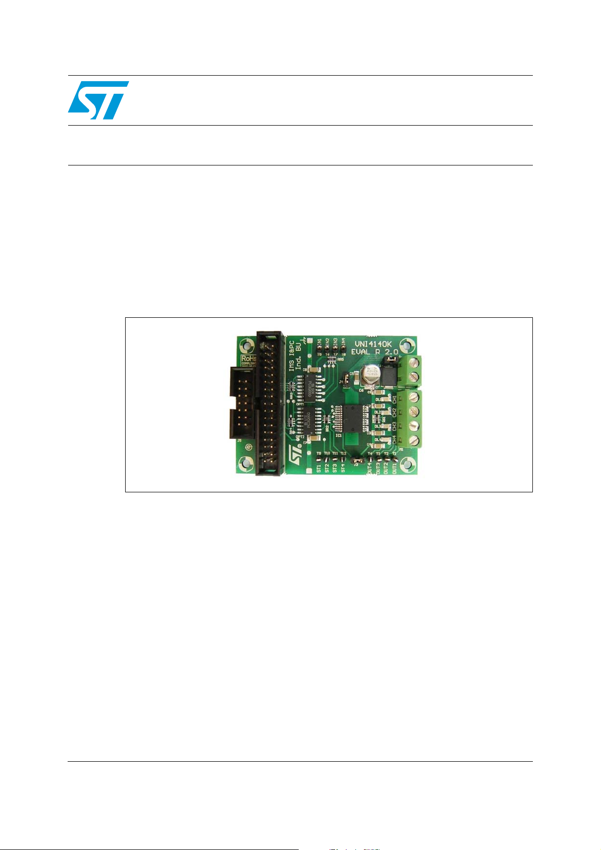
The STEVAL-IFP006V1 demonstration board has been developed to show the new
VNI4140K device functionalities within industrial applications such as PLCs (programmable
logic controllers) which drive lamps, valves, relays, and similar loads.
This tool allows evaluating VNI4140K features, in particular all kinds of embedded selfprotections, power-handling capabilities, operation and diagnostic feedback, thermal
behavior and conformity to inherent IEC standards.
Figure 1. STEVAL-IFP006V1
A double-sided PCB allows obtaining the best trade-off between a routing solution and
thermal management results.
The main features of the demonstration board are:
■ Four output channels (4 x 0.7 A)
■ Four input channels
■ Four feedback channels for diagnostic purposes
■ Bidirectional opto-isolated interface for MCU safe connection
■ TTL/CMOS compatible signals for MCU direct connection
■ LEDs to indicate output state
■ Compliance to IEC61000-4-4 and IEC61000-4-5
May 2009 Doc ID 14266 Rev 1 1/21
■ Compatibility with existing STMicroelectronics tools (IBU communication board,
CANIC10…)
■ 10.5 V to 36 V DC power supply voltage range
www.st.com

Contents AN2684
Contents
1 Electrical characteristics . . . . . . . . . . . . . . . . . . . . . . . . . . . . . . . . . . . . . 4
2 Safety precautions . . . . . . . . . . . . . . . . . . . . . . . . . . . . . . . . . . . . . . . . . . 5
3 VNI4140K quad high-side smart power solid-state relay IC
description . . . . . . . . . . . . . . . . . . . . . . . . . . . . . . . . . . . . . . . . . . . . . . . . . 6
4 IFP006V1 demonstration board description . . . . . . . . . . . . . . . . . . . . . . 8
4.1 Overview . . . . . . . . . . . . . . . . . . . . . . . . . . . . . . . . . . . . . . . . . . . . . . . . . . 8
4.2 IFP006V1 schematic . . . . . . . . . . . . . . . . . . . . . . . . . . . . . . . . . . . . . . . . . 9
4.3 IFP006V1 connectors . . . . . . . . . . . . . . . . . . . . . . . . . . . . . . . . . . . . . . . . 10
4.4 IFP006V1 thermal management . . . . . . . . . . . . . . . . . . . . . . . . . . . . . . . 11
4.5 EMC immunity test . . . . . . . . . . . . . . . . . . . . . . . . . . . . . . . . . . . . . . . . . . 12
4.5.1 Description . . . . . . . . . . . . . . . . . . . . . . . . . . . . . . . . . . . . . . . . . . . . . . . 12
4.5.2 Test conditions . . . . . . . . . . . . . . . . . . . . . . . . . . . . . . . . . . . . . . . . . . . . 12
4.5.3 Burst immunity test . . . . . . . . . . . . . . . . . . . . . . . . . . . . . . . . . . . . . . . . 13
4.5.4 Surge test . . . . . . . . . . . . . . . . . . . . . . . . . . . . . . . . . . . . . . . . . . . . . . . 14
Appendix A Bill of material . . . . . . . . . . . . . . . . . . . . . . . . . . . . . . . . . . . . . . . . . . 16
Appendix B PCB layout . . . . . . . . . . . . . . . . . . . . . . . . . . . . . . . . . . . . . . . . . . . . . 18
Appendix C References . . . . . . . . . . . . . . . . . . . . . . . . . . . . . . . . . . . . . . . . . . . . . 19
Revision history . . . . . . . . . . . . . . . . . . . . . . . . . . . . . . . . . . . . . . . . . . . . . . . . . . . . 20
2/21 Doc ID 14266 Rev 1

AN2684 List of figures
List of figures
Figure 1. STEVAL-IFP006V1. . . . . . . . . . . . . . . . . . . . . . . . . . . . . . . . . . . . . . . . . . . . . . . . . . . . . . . . 1
Figure 2. Block diagram . . . . . . . . . . . . . . . . . . . . . . . . . . . . . . . . . . . . . . . . . . . . . . . . . . . . . . . . . . . . 6
Figure 3. IFP006V1 top view . . . . . . . . . . . . . . . . . . . . . . . . . . . . . . . . . . . . . . . . . . . . . . . . . . . . . . . . 8
Figure 4. IFP006V1 bottom view . . . . . . . . . . . . . . . . . . . . . . . . . . . . . . . . . . . . . . . . . . . . . . . . . . . . . 8
Figure 5. IFP006V1 schematic. . . . . . . . . . . . . . . . . . . . . . . . . . . . . . . . . . . . . . . . . . . . . . . . . . . . . . . 9
Figure 6. J1 connector pinout . . . . . . . . . . . . . . . . . . . . . . . . . . . . . . . . . . . . . . . . . . . . . . . . . . . . . . 10
Figure 7. J5 connector pinout . . . . . . . . . . . . . . . . . . . . . . . . . . . . . . . . . . . . . . . . . . . . . . . . . . . . . . 10
Figure 8. IFP006V1 PCB copper heatsink . . . . . . . . . . . . . . . . . . . . . . . . . . . . . . . . . . . . . . . . . . . . . 11
Figure 9. Thermal map in steady state condition . . . . . . . . . . . . . . . . . . . . . . . . . . . . . . . . . . . . . . . . 11
Figure 10. Thermal map in demagnetization condition (1 Hz repetitive cycling on 48 W 1.2 H load) . 11
Figure 11. Steady state thermal behavior 3D simulation . . . . . . . . . . . . . . . . . . . . . . . . . . . . . . . . . . . 12
Figure 12. Repetitive demagnetization thermal behavior 3D simulation (1 Hz repetitive cycling on
48 W 1.2 H load) . . . . . . . . . . . . . . . . . . . . . . . . . . . . . . . . . . . . . . . . . . . . . . . . . . . . . . . . . 12
Figure 13. Burst timing waveform . . . . . . . . . . . . . . . . . . . . . . . . . . . . . . . . . . . . . . . . . . . . . . . . . . . . 13
Figure 14. Surge standard timing waveform . . . . . . . . . . . . . . . . . . . . . . . . . . . . . . . . . . . . . . . . . . . . 14
Figure 15. IFP006V1 component layer . . . . . . . . . . . . . . . . . . . . . . . . . . . . . . . . . . . . . . . . . . . . . . . . 18
Figure 16. IFP006V1 copper top layer . . . . . . . . . . . . . . . . . . . . . . . . . . . . . . . . . . . . . . . . . . . . . . . . . 18
Figure 17. IFP006V1 copper bottom layer . . . . . . . . . . . . . . . . . . . . . . . . . . . . . . . . . . . . . . . . . . . . . . 18
Doc ID 14266 Rev 1 3/21
Electrical characteristics AN2684
1 Electrical characteristics
The electrical characteristics of the VNI4140k demonstration board (STEVAL-IFP006V1)
are given in Tab l e 1 .
Table 1. STEVAL-IFP006V1 electrical characteristics
Parameter Value Notes
Min Typ Max
Operating conditions
Ambient operating temperature 85 °C
If the VNI4140K junction temperature
exceeds 180 °C, device shuts down
Power supply
Vcc supply voltage 10.5 V 24 V 36 V
Vdd logic supply voltage 5 V From eval communication board
250 µA All channels in OFF state
Supply current on Vdd
2.4 mA 4.8 mA ON state with V
= 5 V
in
Output stage
Output channel ON current limitation 0.7 A 1.7 A
IC internally limited
V
CC = 24 V; RLOAD < 10 mΩ
Maximum DC output current 1.4 A Dynamic load
dV/dt(ON) turn-on voltage slope 0.7 V/µs IOUT = 0.5 A, resistive load
(off) turn-off voltage slope 1.5 V/µs IOUT = 0.5 A, resistive load
dV/dt
Demagnetization protection
Output voltage on inductive turn-off V
CC-41 VCC-45 VCC-50 IOUT = 0.5 A; LLOAD >= 1 mH
4/21 Doc ID 14266 Rev 1

AN2684 Safety precautions
2 Safety precautions
The board must be used only by expert technicians. The copper areas around the
VNI4140K device have a heat sink function, visible in the top layer layout view, refer to
Figure 8. In case of short-circuit, current limiting or hard demagnetization, the STEVAL-
IFP006V1 board, or part of it, might reach a very high temperature with consequent danger.
No specific protections are implemented for reverse DC accidental connection. Remember
that an electrolytic capacitor is connected to the supply bus, therefore a reverse continuous
DC voltage applied to it may produce a dangerous explosion.
Warning: ST assumes no responsibility for any consequences which
may result from the improper use of this tool.
Doc ID 14266 Rev 1 5/21
VNI4140K quad high-side smart power solid-state relay IC description AN2684
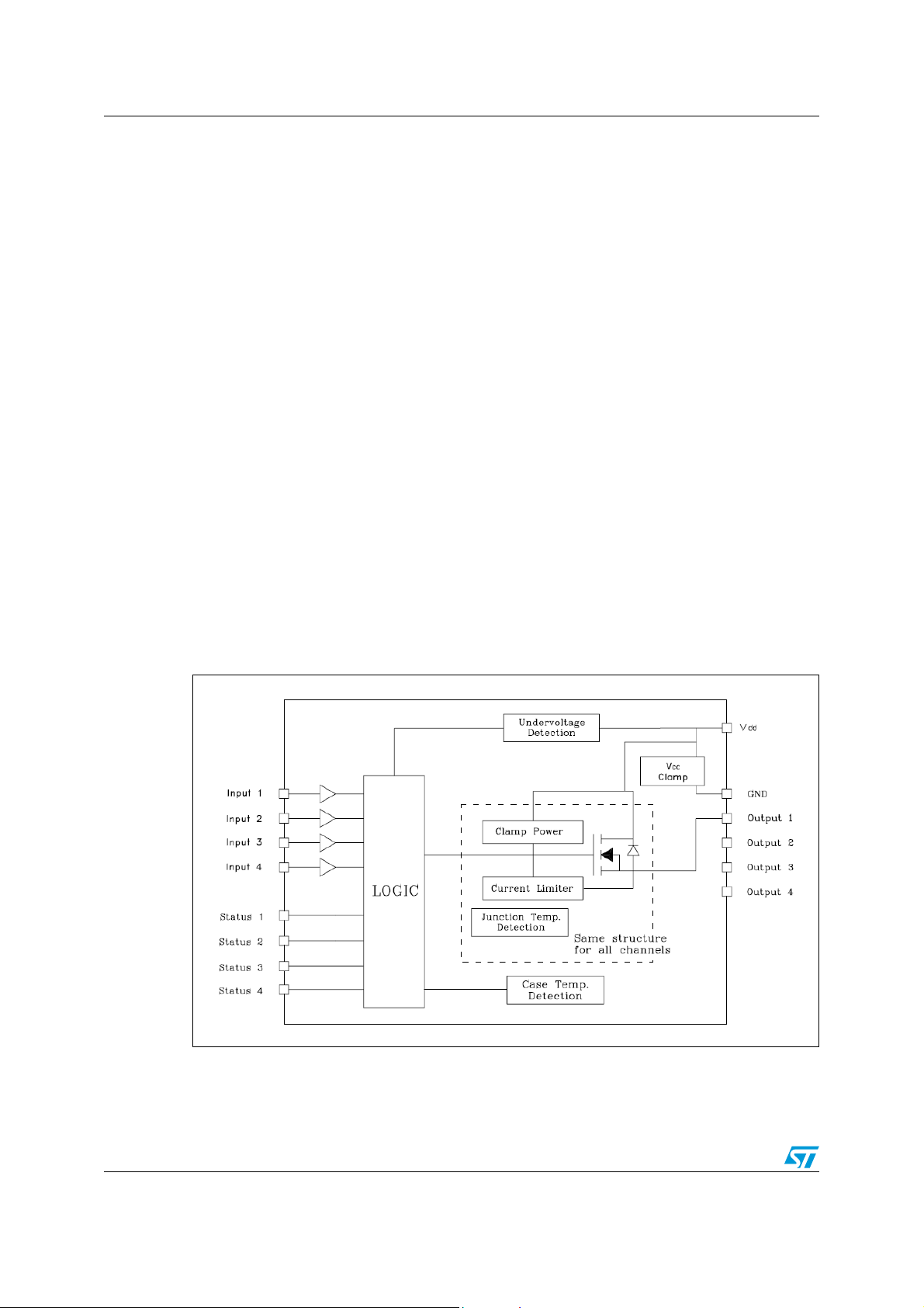
3 VNI4140K quad high-side smart power solid-state
relay IC description
The VNI4140k is a monolithic 4-channel driver featuring a very low supply current. The IC,
which uses STMicroelectronics VIPower technology, is intended for driving loads with one
side connected to ground.
Active channel current limitation, combined with thermal shutdown (independent for each
channel) and automatic restart, protect the device against overload.
The main features of the VNI4140K IC are:
● Output current: 0.7 A per channel
● Shorted load protections for each channel
● Junction overtemperature protection
● Case overtemperature protection for thermal independence of the channels
● Thermal case shutdown and restart not simultaneous for the various channels
● Protection against ground disconnection
● Current limitation
● Undervoltage shutdown
● Open drain diagnostic outputs
● 3.3 V CMOS/TTL compatible inputs
● Fast demagnetization of inductive loads
● Conforms to IEC 61131-2
Figure 2. Block diagram
Active current limitation avoids that the system power supply drops in case of shorted load.
In overload condition, the channel turns OFF and back ON automatically after the IC
temperatures decrease below a threshold fixed by a temperature hysteresis so that junction
6/21 Doc ID 14266 Rev 1

AN2684 VNI4140K quad high-side smart power solid-state relay IC description
temperature is controlled. If this condition makes the case temperature reach the case
temperature limit (T
has exceeded the junction protection threshold, T
protection reset threshold, T
only when the case temperature decreases below the case protection reset threshold (T
), overloaded channels (i.e. the ones for which junction temperature
CSD
) are turned OFF. These channels restart, non-simultaneously,
jR
, and has not fallen below the junction
jSD
CR
).
Non-overloaded channels continue to operate normally.
The open drain diagnostic outputs indicate related channel overtemperature conditions.
Doc ID 14266 Rev 1 7/21

IFP006V1 demonstration board description AN2684
4 IFP006V1 demonstration board description
4.1 Overview
The VNI4140K demonstration board is composed of two main sections:
● Opto-isolated interface for input and status signals
● A four-channel self-protect power stage section with STMicroelectronics Tr an si l™
diode protection
The demonstration board consists of a double-sided FR4 printed circuit board with 35 µm
copper plating. The PCB dimensions are 52 mm x 68 mm. The top and bottom views are
shown below.
Figure 3. IFP006V1 top view
Figure 4. IFP006V1 bottom view
8/21 Doc ID 14266 Rev 1

AN2684 IFP006V1 demonstration board description
4.2 IFP006V1 schematic
Figure 5. IFP006V1 schematic
C8
4.7nF
GND
+24Vdc
M2
C7
4.7nF
OPEN
STAT4STAT3
STAT2STAT1
M.2VITEB
1
2
J2
A B
FOR
OVL TEST
C6
47uF
+
C5
100nF
1206
T1
T2
D1
SM15T39AC
C1
10nF LV
1206
20
21
C2
T3
10nF LV
IC1
1206
OUT1
123
C3
OUT3
OUT2
4
T4
10nF LV
1206
OUT4
M1
M.4VITEB
13
1206
DL1
DL2
DL3
DL4
VNI4140K
LED
LED
LED
LED
10nF LV
RR1
C4
10K 1206
1 2
VDD
1 2
OUT2_b
3 4
5 6
7 8
9 10
11 12
13 14
J5
CAN7
IN1 IN2
IN3 IN4
RR5
47K 1206
OR
J4
Vcc DISC. TEST
CURRENT PROBE
TAB
A B
OUT1_a24OUT1_b23OUT1_c22OUT2_a
Vcc
IN1
Vcc
2
1
T5
IN2
4
T6
OUT2_c19OUT3_a18OUT3_b17OUT3_c16OUT4_a15OUT4_b14OUT4_c
VNI4140K
IN38IN4
10
J3
GND
STAT1
STAT37STAT4
STAT2
3
9
5
GND DISC. TEST
6
A B
T12
T11
T10
T9
T7
RR2
T8
10
11
12
13
14
15
16
STAT1
1234567
3 4
5 6
7 8
9 10
11 12
13 14
15 16
17 18
19 20
21 22
23 24
25 26
27 28
29 30
31 32
33 34
J1
EVALCOMMBOARD
8 9
RR3
1K 1206
OPT1
TLP281-4
89
10111213141516
10K 1206
1234567
OPT2
TLP281-4
IN1
IN2
IN3
IN4
VDD
STAT4
STAT3
STAT2
IN1
IN2
IN3
IN4
STAT1
STAT2
STAT3
STAT4
RR4
VDD
10K 1206
Doc ID 14266 Rev 1 9/21

IFP006V1 demonstration board description AN2684
4.3 IFP006V1 connectors
The demonstration board is equipped with input and output connectors. Specifically, there
are two input header connectors (J5 and J1), one 4-channel output connector (M1), and a
supply voltage connector (M2).
Both input connectors, J5 and J1, provide the same bidirectional signals guaranteeing the
maximum compatibility with existing STMicroelectronics tools such as the industrial
communication board (see AN2451) and similar products.
Figure 6. J1 connector pinout
Figure 7. J5 connector pinout
Table 2. J1 and J5 pin description
J1 pin number J5 pin number Signal Type
11 1 Vdd 5/3.3 V supply voltage
23 2 GND Signal ground
9 3 IN1 Input channel 1
13 4 IN2 Input channel 2
15 5 IN3 Input channel 3
17 6 IN4 Input channel 4
6 7 STAT1 Status channel 1
25 8 STAT2 Status channel 2
21 9 STAT3 Status channel 3
19 10 STAT4 Status channel 4
10/21 Doc ID 14266 Rev 1

AN2684 IFP006V1 demonstration board description
4.4 IFP006V1 thermal management
The IFP006V1 PCB has two heatsinks: approximately 1 sq. cm on the top layer and 3 sq.
cm on the bottom layer, thermally interconnected through 9 vias, as shown in Figure 8.
In a steady state condition low R
ensures a very low dissipation but in current
DS(on)
limitation and in fast demagnetization, the power dissipation is much higher, requiring a low
thermal resistance through the device exposed tab, soldering space, top layer, vias and
bottom layer path. A 35 µm copper (10 oz/sq. ft) thickness and 0.3 mm diameter for the vias
are used according to EIA/JESD51-5.
Figure 8. IFP006V1 PCB copper heatsink
Figure 9 and 11 show the IFP006V1 temperature map with all channels permanently
switched ON, 48 Ω loads, 24 V supply voltage and ambient temperature of 25 °C. The IC
temperature increase is only about a few degrees.
Figure 10 and 12 show a similar map when the IC is cycling at 1 Hz, 50% duty cycle, 48 Ω
1.2 H loads, 24 V supply voltage and ambient temperature of 25 °C.
Figure 9. Thermal map in steady state
condition
Figure 10. Thermal map in demagnetization
condition (1 Hz repetitive cycling on
48 Ω 1.2 H load)
AM01851v1
Doc ID 14266 Rev 1 11/21
AM01852v1

IFP006V1 demonstration board description AN2684
Figure 11. Steady state thermal behavior 3D
simulation
AM01853v1
In particular Figure 11 and 12 show 3D thermal modelization of the device.
4.5 EMC immunity test
4.5.1 Description
Figure 12. Repetitive demagnetization thermal
behavior 3D simulation (1 Hz
repetitive cycling on 48 Ω 1.2 H
load)
AM01854v1
IFP006V1 has been tested according to EMC immunity standards IEC61000-4-4 (fast
transient burst) and IEC61000-4-5 (high energy surge).
A fast transient burst test has been performed all channels.
Each channel under test is cycling ON and OFF at 1 Hz, duty cycle 50%, on four 48 Ω load
resistors at 24 Vdc supply voltage.
A burst signal was applied using an ultra-compact simulator with an internal capacitive
coupling clamp tool.
4.5.2 Test conditions
● Ambient temperature: 25.6 °C
● Ambient humidity: 46%
● Main voltage power supply: 24 Vdc
● DC insulated voltage: 5 Vdc
● Loads: 4 x 48 Ω power resistor
12/21 Doc ID 14266 Rev 1

AN2684 IFP006V1 demonstration board description
4.5.3 Burst immunity test
Tab le 3 gives the burst setup configuration adopted to perform this test.
Table 3. Burst setup configuration
Test level Condition
Pulse time rt 5 ns ± 30%
Pulse duration td 50 ns ± 30%
Source impedance Zq = 50 Ω ± 20%
Polarity Positive / negative
Burst duration (td) 15 ms ± 20%
Burst frequency (f) 5 kHz
Burst period (tr) 300 ms ± 20%
Duration time (T) 5 min
Figure 13 below shows the standard timing waveform applied during the burst test.
Figure 13. Burst timing waveform
Tab le 4 shows the results of an inherent burst test. Normal performance has been observed
when applying four different disturbance levels on the output ports and Vcc main voltage
power supply.
Doc ID 14266 Rev 1 13/21

IFP006V1 demonstration board description AN2684
Table 4. Burst test results
Burst standard test routines Level Voltage (kV) Acceptance criteria
(1)
IEC 61000-4-4 Level 1 0.5 A
IEC 61000-4-4 Level 2 1 A
IEC 61000-4-4 Level 3 2 A
IEC 61000-4-4 Level 4 4 A
1. Classification of the test
(Criteria A): normal performance
(Criteria B): temporary degradation or loss of function or performance with automatic return to normal operation
(Criteria C): temporary degradation or loss of function with external intervention to recover normal operation
(Criteria D): degradation or loss of function, need replacement of damaged components to recover normal
operation.
4.5.4 Surge test
A high energy surge test was performed in differential mode. A high surge signal was
injected on the DUT (device under test) through a 42 Ω decoupling resistor. The test
consisted of three positive and three negative discharges with a repetition rate of 1
discharge per minute.
Figure 14 shows the standard timing waveform applied on the DUT.
Figure 14. Surge standard timing waveform
Tab le 5 below shows normal performance of the device.
14/21 Doc ID 14266 Rev 1

AN2684 IFP006V1 demonstration board description
Table 5. Surge test results
Surge standard test
routines
Level Voltage (V) Acceptance criteria
IEC 61000-4-5 Level 1 500 A
IEC 61000-4-5 Level 2 1000 A
IEC 61000-4-5 Level 3 2000 A
1. Classification of the test
(Criteria A): normal performance
(Criteria B): temporary degradation or loss of function or performance with automatic return to normal operation
(Criteria C): temporary degradation or loss of function with external intervention to recover normal operation
(Criteria D): degradation or loss of function, need replacement of damaged components to recover normal
operation.
(1)
Doc ID 14266 Rev 1 15/21

Bill of material AN2684
Appendix A Bill of material
Table 6. IFP006V1 demonstration board bill of material
Designator Part type Description
RR1 10 kΩ x 4 SMD resistor pack 1206 format
RR2 10 kΩ x 4 SMD resistor pack 1206 format
RR3 1 kΩ x 4 SMD resistor pack 1206 format
RR4 10 kΩ x 4 SMD resistor pack 1206 format
RR5 47 kΩ x 4 SMD resistor pack 1206 format
C1 10 nF LV SMD capacitor 1206 format
C2 10 nF LV SMD capacitor 1206 format
C3 10 nF LV SMD capacitor 1206 format
C4 10 nF LV SMD capacitor 1206 format
C5 100 nF SMD capacitor 1206 format
C6 47 µF 50 V SMD electrolytic capacitor
C7 4.7 nF SMD capacitor 1206 format
C8 4.7 nF SMD capacitor 1206 format
D1 SM15T39AC Transil™ diode
DL1 LED diode SMD LED diode 0805 format
DL2 LED diode SMD LED diode 0805 format
DL3 LED diode SMD LED diode 0805 format
DL4 LED diode SMD LED diode 0805 format
OPT1 PC3Q66Q 4-channel OPTO isolator
OPT2 PC3Q66Q 4-channel OPTO isolator
IC1 VNI4140K ST IC Industrial 4 CH HSD
J1 HADER 34-pin Compatible EVALCOMMBOARD
J2 Jumper Overvoltage test
J3 Jumper Ground disconnection test
J4 Jumper V
disconnection test
cc
J5 Hader 14-pin Compatible ST7CANIC DB
M1 4 screw plugs HSD output connector
M2 2 screw plugs Power supply connector
T1 Test point HSD output channel 1 voltage
T2 Test point HSD output channel 2 voltage
T3 Test point HSD output channel 3 voltage
T4 Test point HSD output channel 4 voltage
16/21 Doc ID 14266 Rev 1

AN2684 Bill of material
Table 6. IFP006V1 demonstration board bill of material (continued)
Designator Part type Description
T5 Test point HSD input channel 1 signal
T6 Test point HSD input channel 2 signal
T7 Test point HSD input channel 3 signal
T8 Test point HSD input channel 4 signal
T9 Test point HSD channel 1 status
T10 Test point HSD channel 2 status
T11 Test point HSD channel 3 status
T12 Test point HSD channel 4 status
Doc ID 14266 Rev 1 17/21

PCB layout AN2684
Appendix B PCB layout
Figure 15. IFP006V1 component layer
Figure 16. IFP006V1 copper top layer Figure 17. IFP006V1 copper bottom layer
18/21 Doc ID 14266 Rev 1

AN2684 References
Appendix C References
1. AN1351 - VIPower and BCDmultipower: making life easier with ST's high side drivers
Doc ID 14266 Rev 1 19/21

Revision history AN2684
Revision history
Table 7. Document revision history
Date Revision Changes
20-May-2009 1 Initial release
20/21 Doc ID 14266 Rev 1

AN2684
Please Read Carefully:
Information in this document is provided solely in connection with ST products. STMicroelectronics NV and its subsidiaries (“ST”) reserve the
right to make changes, corrections, modifications or improvements, to this document, and the products and services described herein at any
time, without notice.
All ST products are sold pursuant to ST’s terms and conditions of sale.
Purchasers are solely responsible for the choice, selection and use of the ST products and services described herein, and ST assumes no
liability whatsoever relating to the choice, selection or use of the ST products and services described herein.
No license, express or implied, by estoppel or otherwise, to any intellectual property rights is granted under this document. If any part of this
document refers to any third party products or services it shall not be deemed a license grant by ST for the use of such third party products
or services, or any intellectual property contained therein or considered as a warranty covering the use in any manner whatsoever of such
third party products or services or any intellectual property contained therein.
UNLESS OTHERWISE SET FORTH IN ST’S TERMS AND CONDITIONS OF SALE ST DISCLAIMS ANY EXPRESS OR IMPLIED
WARRANTY WITH RESPECT TO THE USE AND/OR SALE OF ST PRODUCTS INCLUDING WITHOUT LIMITATION IMPLIED
WARRANTIES OF MERCHANTABILITY, FITNESS FOR A PARTICULAR PURPOSE (AND THEIR EQUIVALENTS UNDER THE LAWS
OF ANY JURISDICTION), OR INFRINGEMENT OF ANY PATENT, COPYRIGHT OR OTHER INTELLECTUAL PROPERTY RIGHT.
UNLESS EXPRESSLY APPROVED IN WRITING BY AN AUTHORIZED ST REPRESENTATIVE, ST PRODUCTS ARE NOT
RECOMMENDED, AUTHORIZED OR WARRANTED FOR USE IN MILITARY, AIR CRAFT, SPACE, LIFE SAVING, OR LIFE SUSTAINING
APPLICATIONS, NOR IN PRODUCTS OR SYSTEMS WHERE FAILURE OR MALFUNCTION MAY RESULT IN PERSONAL INJURY,
DEATH, OR SEVERE PROPERTY OR ENVIRONMENTAL DAMAGE. ST PRODUCTS WHICH ARE NOT SPECIFIED AS "AUTOMOTIVE
GRADE" MAY ONLY BE USED IN AUTOMOTIVE APPLICATIONS AT USER’S OWN RISK.
Resale of ST products with provisions different from the statements and/or technical features set forth in this document shall immediately void
any warranty granted by ST for the ST product or service described herein and shall not create or extend in any manner whatsoever, any
liability of ST.
ST and the ST logo are trademarks or registered trademarks of ST in various countries.
Information in this document supersedes and replaces all information previously supplied.
The ST logo is a registered trademark of STMicroelectronics. All other names are the property of their respective owners.
© 2009 STMicroelectronics - All rights reserved
STMicroelectronics group of companies
Australia - Belgium - Brazil - Canada - China - Czech Republic - Finland - France - Germany - Hong Kong - India - Israel - Italy - Japan -
Malaysia - Malta - Morocco - Philippines - Singapore - Spain - Sweden - Switzerland - United Kingdom - United States of America
www.st.com
Doc ID 14266 Rev 1 21/21
 Loading...