

Page 1
AN2683
Application note
Compact dual output point of load converter
based on the PM6680 step-down controller
Introduction
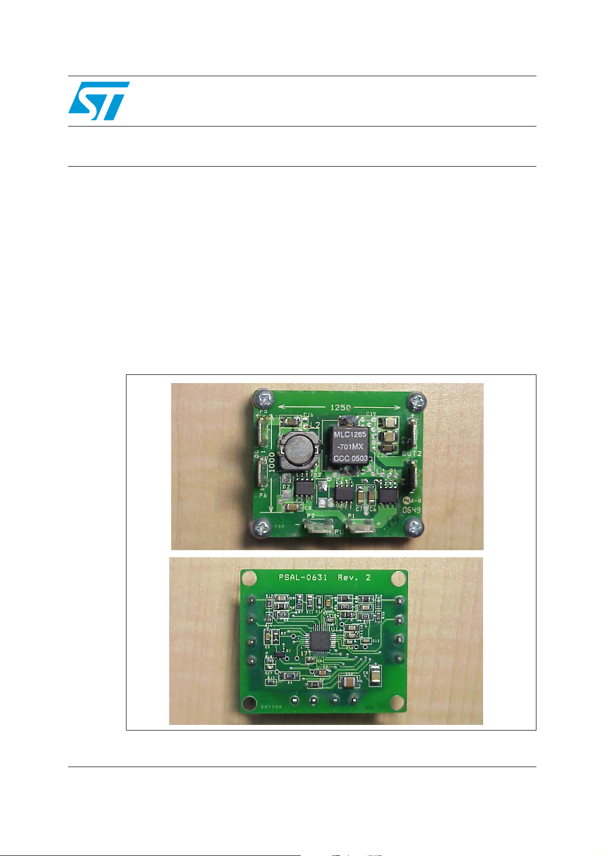
This application note demonstrates the performance of the PM6680 dual step-down
controller by implementing a two output point of load converter in a small printed circuit
board footprint. Utilizing constant on-time architecture and featuring a no-audio skip mode of
operation, a common bus voltage that ranges between 10 to 16 V
at 10.5 amps and 1.8 V
no-audio skip feature significantly improves efficiency at light load. Using surface mount
components on both the top and bottom of the circuit board and featuring ceramic output
capacitors, the area needed for the converter measures only 1.0 by 1.25 inches (25.4 by
37.75 mm). The method for component value dimensioning is described along with the
schematic and construction details. Typical efficiencies and functional test data are also
presented.
Figure 1. PM6680 - top and bottom view
at 2.5 amps for a total output power level of 15 watts. The unique
DC
is converted to 1.0 VDC
DC
April 2008 Rev 1 1/38
www.st.com
Page 2

Contents AN2683
Contents
1 Main characteristics . . . . . . . . . . . . . . . . . . . . . . . . . . . . . . . . . . . . . . . . . 5
1.1 Input voltage range . . . . . . . . . . . . . . . . . . . . . . . . . . . . . . . . . . . . . . . . . . . 5
1.2 Output ripple voltage . . . . . . . . . . . . . . . . . . . . . . . . . . . . . . . . . . . . . . . . . 5
1.3 Switching frequency . . . . . . . . . . . . . . . . . . . . . . . . . . . . . . . . . . . . . . . . . . 5
1.4 Output overload/short circuit . . . . . . . . . . . . . . . . . . . . . . . . . . . . . . . . . . . 5
2 Circuit description . . . . . . . . . . . . . . . . . . . . . . . . . . . . . . . . . . . . . . . . . . . 6
3 Construction . . . . . . . . . . . . . . . . . . . . . . . . . . . . . . . . . . . . . . . . . . . . . . 21
4 Functional testing . . . . . . . . . . . . . . . . . . . . . . . . . . . . . . . . . . . . . . . . . . 26
4.1 Input/output voltage . . . . . . . . . . . . . . . . . . . . . . . . . . . . . . . . . . . . . . . . . 28
4.2 Ripple/noise voltage . . . . . . . . . . . . . . . . . . . . . . . . . . . . . . . . . . . . . . . . . 28
4.3 Load transient overshoot . . . . . . . . . . . . . . . . . . . . . . . . . . . . . . . . . . . . . 28
4.4 Output current limit . . . . . . . . . . . . . . . . . . . . . . . . . . . . . . . . . . . . . . . . . . 33
4.5 Output short circuit . . . . . . . . . . . . . . . . . . . . . . . . . . . . . . . . . . . . . . . . . . 33
4.6 Input under voltage lockout . . . . . . . . . . . . . . . . . . . . . . . . . . . . . . . . . . . 33
5 Bill of material . . . . . . . . . . . . . . . . . . . . . . . . . . . . . . . . . . . . . . . . . . . . . 35
6 Revision history . . . . . . . . . . . . . . . . . . . . . . . . . . . . . . . . . . . . . . . . . . . 37
2/38
Page 3

AN2683 List of figures
List of figures
Figure 1. PM6680 - top and bottom view . . . . . . . . . . . . . . . . . . . . . . . . . . . . . . . . . . . . . . . . . . . . . . . 1
Figure 2. Circuit board schematic . . . . . . . . . . . . . . . . . . . . . . . . . . . . . . . . . . . . . . . . . . . . . . . . . . . . 7
Figure 3. Components of virtual ESR network. . . . . . . . . . . . . . . . . . . . . . . . . . . . . . . . . . . . . . . . . . 13
Figure 4. Top layer component placement . . . . . . . . . . . . . . . . . . . . . . . . . . . . . . . . . . . . . . . . . . . . 21
Figure 5. Top layer copper . . . . . . . . . . . . . . . . . . . . . . . . . . . . . . . . . . . . . . . . . . . . . . . . . . . . . . . . . 22
Figure 6. Inner layer 1 showing additional power traces . . . . . . . . . . . . . . . . . . . . . . . . . . . . . . . . . . 22
Figure 7. Power ground layer (inner layer 2) . . . . . . . . . . . . . . . . . . . . . . . . . . . . . . . . . . . . . . . . . . . 23
Figure 8. Signal ground layer (inner layer 3) . . . . . . . . . . . . . . . . . . . . . . . . . . . . . . . . . . . . . . . . . . . 23
Figure 9. Bottom layer components placement (mirrored). . . . . . . . . . . . . . . . . . . . . . . . . . . . . . . . . 24
Figure 10. Bottom layer copper (mirrored). . . . . . . . . . . . . . . . . . . . . . . . . . . . . . . . . . . . . . . . . . . . . . 24
Figure 11. Inner layer 4 (mirrored) . . . . . . . . . . . . . . . . . . . . . . . . . . . . . . . . . . . . . . . . . . . . . . . . . . . . 25
Figure 12. Efficiency vs. load current in PWM mode (1.0 V) . . . . . . . . . . . . . . . . . . . . . . . . . . . . . . . . 26
Figure 13. Efficiency vs. load current in NA-skip mode (1.0 V) . . . . . . . . . . . . . . . . . . . . . . . . . . . . . . 26
Figure 14. Efficiency vs. load current in PWM mode (1.8 V) . . . . . . . . . . . . . . . . . . . . . . . . . . . . . . . . 27
Figure 15. Efficiency vs. load current in NA-skip mode (1.8 V) . . . . . . . . . . . . . . . . . . . . . . . . . . . . . . 27
Figure 16. V
Figure 17. V
Figure 18. V
Figure 19. V
Figure 20. V
Figure 21. V
output - 100% to 50% load change (20µs/div) . . . . . . . . . . . . . . . . . . . . . . . . . . . . . . 29
DC
output - 50% to 100% load change (20µs/div) . . . . . . . . . . . . . . . . . . . . . . . . . . . . . . 30
DC
output - 20% to 80% step load change (50µs/div). . . . . . . . . . . . . . . . . . . . . . . . . . . . 30
DC
output - 100% to 50% load change (20µs/div) . . . . . . . . . . . . . . . . . . . . . . . . . . . . . . 31
DC
output - 50% to 100% load change (20µs/div) . . . . . . . . . . . . . . . . . . . . . . . . . . . . . . 32
DC
output - 20% to 80% step load change (50µs/div). . . . . . . . . . . . . . . . . . . . . . . . . . . . 32
DC
3/38
Page 4

List of tables AN2683
List of tables
Table 1. Input voltage range 10 - 16 VDC . . . . . . . . . . . . . . . . . . . . . . . . . . . . . . . . . . . . . . . . . . . . . 5
Table 2. 1.0 V
Table 3. 1.8 V
Table 4. 1.0 V
Table 5. 1.8 V
Table 6. 1.0 V
Table 7. 1.8 V
Table 8. 1.0 V
Table 9. 1.8 V
Table 10. 1.0 V
Table 11. 1.8 V
Table 12. Part list . . . . . . . . . . . . . . . . . . . . . . . . . . . . . . . . . . . . . . . . . . . . . . . . . . . . . . . . . . . . . . . . 35
Table 13. Document revision history . . . . . . . . . . . . . . . . . . . . . . . . . . . . . . . . . . . . . . . . . . . . . . . . . 37
output . . . . . . . . . . . . . . . . . . . . . . . . . . . . . . . . . . . . . . . . . . . . . . . . . . . . . . . . . . 28
DC
output . . . . . . . . . . . . . . . . . . . . . . . . . . . . . . . . . . . . . . . . . . . . . . . . . . . . . . . . . . 28
DC
output . . . . . . . . . . . . . . . . . . . . . . . . . . . . . . . . . . . . . . . . . . . . . . . . . . . . . . . . . . 28
DC
output . . . . . . . . . . . . . . . . . . . . . . . . . . . . . . . . . . . . . . . . . . . . . . . . . . . . . . . . . . 28
DC
output . . . . . . . . . . . . . . . . . . . . . . . . . . . . . . . . . . . . . . . . . . . . . . . . . . . . . . . . . . 29
DC
output . . . . . . . . . . . . . . . . . . . . . . . . . . . . . . . . . . . . . . . . . . . . . . . . . . . . . . . . . . 31
DC
output . . . . . . . . . . . . . . . . . . . . . . . . . . . . . . . . . . . . . . . . . . . . . . . . . . . . . . . . . . 33
DC
output . . . . . . . . . . . . . . . . . . . . . . . . . . . . . . . . . . . . . . . . . . . . . . . . . . . . . . . . . . 33
DC
output . . . . . . . . . . . . . . . . . . . . . . . . . . . . . . . . . . . . . . . . . . . . . . . . . . . . . . . . . . 34
DC
output . . . . . . . . . . . . . . . . . . . . . . . . . . . . . . . . . . . . . . . . . . . . . . . . . . . . . . . . . . 34
DC
4/38
Page 5

AN2683 Main characteristics
1 Main characteristics
1.1 Input voltage range
Table 1. Input voltage range 10 - 16 V
Output Nominal voltage VDC Max. current amp Regulation %
11.8 2.5 0.44
2 1.0 10.5 2.6
1. Regulation over entire line and load range
1.2 Output ripple voltage
● Output 1: 45 mV p-p at maximum output current
● Output 2: 30 mV p-p at maximum output current
1.3 Switching frequency
● Output 1: 1 - 300 kHz
● Output 2: 2 - 400 kHz
1.4 Output overload/short circuit
● Output 1: nominal trip level 3.37 A (135%)
● Output 2: nominal trip level 13.65 A (130%)
DC
(1)
Protection is latched. Power must be cycled to reset.
5/38
Page 6

Circuit description AN2683
2 Circuit description
The PM6680 contains all the control circuitry needed to implement two independent stepdown synchronous buck regulators using the constant on-time method. The constant ontime method, an improved variant of hysteretic control, provides superior transient response
to changes of input voltage and load levels. One of the big advantages of this control
method is that it can provide this quick response without the use of an error amplifier which
in turn eliminates the need for frequency compensation.
As shown in the photographs (Figure 1) all the parts used are surface mount type including
the inductors. The circuit board is a multiple layer type consisting of six layers. The top two
layers are power routing, the middle two are ground layers split as power and signal, and the
bottom two are signal routing layers. In this design, in order to have a low inductor value for
the higher current 10.5 A output side, the PM6680 runs in its intermediate range with output
one running at 300 kHz and output two running at 400 kHz. So as a consequence the 2.5 A
output will run at 300 kHz. With the switching frequencies established the dimensions of the
other components can be defined.
6/38
Page 7
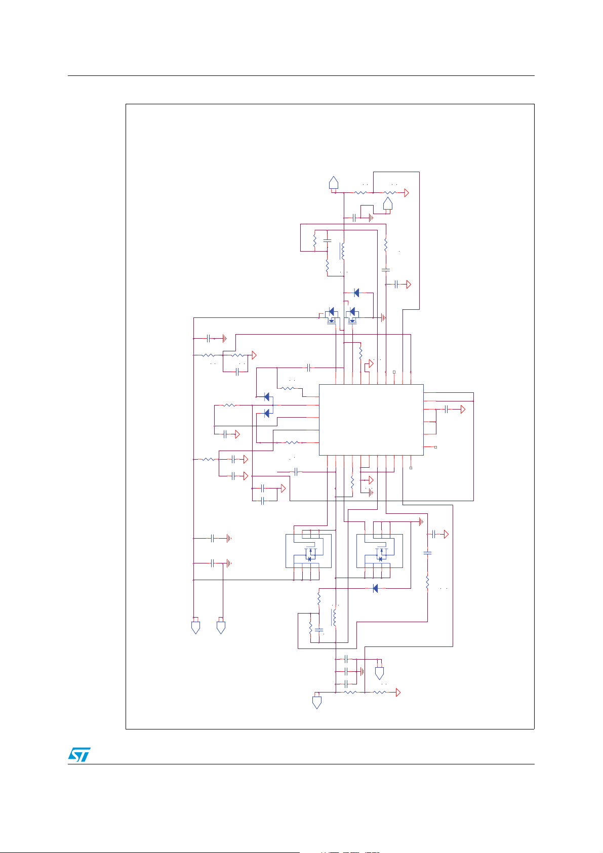
AN2683 Circuit description
Figure 2. Circuit board schematic
Vout 1 - 1.8 VDC @ 2.5 A
QC
P5
R15
10.0k
R16
D2
Open
A
Q3
3
750R
17
Csense1
U1
1
432
V5SW
PM6680
SGnd1
12
R12
1 2
29
30
Out1
Comp1
Out28PGnd14Csense2
2
10.0k
QC
P6
2.55k
C13
330pF
C14
22pF
28
26
5
En2
4
FB1
Shdn
En1
Pgood1
18
25
Vref
32
Skip
C18
24
0.1uF
Fsel
3
nc
6
Pgood2
FB27SGnd216Comp2
27
C12
22pF
C8
12
R17
110k
R4
3R92
1/4W
12
10 uF
12
C4
1%
C7
10 uF
12
R18
C17
R3
1%
47R5 1/8W
0.22uF
C3
0.1uF
C5
4.7uF
12
C16
47uF
C10
1.8nF
R10
3.74k
1 2
STS8DNF3LL
8
7
C1
R1
10R0
R2
432
0.1uF
23
18
31
19
9
10R0
C2
0.1uF
18
30.0k
100pF
D1BAT54A
12
K2
A
K1
12
C21
1uF
C22
4.7uF
2.5 uH
MSS1038
L2
R9
57.6k
1 2
K
5
6
2
4
1
R6
1 2
21
15
20
22
Boot1
Lgate1
Hgate1
Phase1
LD05
Vcc
Vin
Boot2
Phase2
Hgate2
Lgate2
12
11
10
13
R5
750R
1 2
C6
10 uF
P1
P2
QC
QC
-
+
Vin 10.2 - 16.0 VDC
Q1
STS12NH3LL
765
R7
26.1k
1 2
0.7uH
R8
5.11k
1 2
P3
MLC1550L1
C9 1.8n F
100uF
C19
100uF
C15
47uF
C20
12
R13
QC
765
Q2
A K
D3
Open
P4
QC
2
1
R14
1.10k
10.0k
C11
STS25NH3LL
330pF
R11
1.91k
1 2
Vout2 - 1.0 VDC @ 10.5 A
7/38
Page 8

Circuit description AN2683
As a starting point for the value of the inductors we look at the full load current (Ifl) for each
output and let the inductor ripple (I
value of 30 percent is used.
I
= I
* 0.3
r
fl
for
● Output 1: I
● Output 2: I
Then the values of the inductors are calculated using the formula:
Equation 1:
= 0.75 A
r
= 3.15 A
r
) current equal 20 to 30 percent of it. For this design a
r
VinV
L
–
------------------------ -
f
⋅
swIr
out
⋅=
V
out
---------- -
V
in
where V
frequency.
So for input 1:
Equation 2
and for output 2:
Equation 3
The output filter capacitors are roughly approximated so that the change in output voltage
(∆V
output voltage change of two to three percent of the total output voltage is considered
acceptable. The formula used is:
is the nominal input voltage, V
in
12 1.8–
----------------------------------------
L
300kHz 0.75⋅
----------------------------------------
L
400kHz 3.15⋅
) during a positive load transient (load is reduced) is minimized. For this design an
out
the output voltage and fsw the switching
out
1.8
------- -
6.8µH=⋅=
12
12 1–
12
------
1
0.7µH=⋅=
Equation 4
----------------------------------------------------------------
C
>
2VinV
⋅⋅
8/38
LI
⋅
–()ΛV
2
()
fl
out
out
Page 9

AN2683 Circuit description
For output 1 a ∆V
Equation 5
This is a nonstandard value so a 47 µF is used.
For output 2 a ∆V
Equation 6
As the formula indicates the capacitor value should be greater than that calculated. Even
though the board area is small, this section allows the use of ceramic capacitors that are
comprised of two 100 µF and one 47 µF all in parallel and which still fit in the required
footprint.
of 2.5% of 1.8 VDC or 45 mV is used, thus:
out
6.8µH2.5()
46.2µF
of 2% of 1.0 VDC or 20 mV is used:
out
175µF
----------------------------------------------------------
>
2121.8–()0.045⋅⋅
0.7µH 10.5()
----------------------------------------------------------
>
2121.0–()0.020⋅⋅
⋅
⋅
2
2
With these values of capacitors the ripple voltage can be checked. This is dominated by the
equivalent series resistance (ESR) of the capacitors. The ESR must be equal or less than
the value calculated by:
Equation 7:
V
r
ESR
where V
capacitors is given in their datasheets at the frequency they are used at as shown in the
graphs. The value is basically the same at both 300 and 400 kHz. For the 47 µF the ESR is
2 mΩ and for the 100 µF it is 1.5 mΩ. With these values we can calculate the ripple voltage
V
r
Equation 8:
by:
is the output ripple voltage and Ir is the inductor ripple current. The ESR for the
r
V
r
-----
≤
I
r
IrESR⋅=
9/38
Page 10

Circuit description AN2683
for output 1:
Equation 9
0.75A 2mΩ 1.5mV=⋅
for output 2:
Equation 10
3.15A 545µΩ 1.9mV=⋅
These values conform to the specification. They are higher in a practical circuit because of
parasitic inductance and loop resistance. Good circuit board layout techniques are
essential. Additionally, because of the constant on-time control, the system regulates the
output voltage by the valley value of the ripple voltage. A minimum amount of ripple voltage
of 30 mV should be on the comp pin to accomplish this. Since the calculated ripple voltage
is much lower than this, an additional circuit called the virtual ESR network is incorporated
to provide the additional voltage. Before addressing this design, the current limit resistor
values will be established. In this design the R
implement the current limit. For output 1 with its relatively low output current the MOSFET
chosen was the STS8DNF3LL with a nominal R
dual, that is two MOSFETs are contained in the same SO-8 package realizing further circuit
board space savings. The current limit is a valley type that operates during the conduction of
the low side MOSFET. A 100 µA internal current generator connected to the C
along with a resistor establishes a voltage to which the voltage generated by the R
compared. If the R
voltage is greater, then the voltage at the C
DS(on)
of a new conduction cycle is inhibited. The value of Rc
of the lower MOSFETS is used to
DS(on)
of 18 mΩ. This particular part is a
DS(on)
pin the generation
is determined by:
sense
sense
sense
pin
DS(on)
is
Equation 11:
Rc
sense
The 18 mΩ value for R
is a nominal 25 °C number. As current is switched through the
DS(on)
device and the ambient is raised, the R
140% is used. Targeting the maximum output current (I
0.750 A the valley current value is:
10/38
R
DS on()Ivalley
----------------------------------------- -=
⋅
100µA
increases. An increase of approximately
DS(on)
) at 3.375 A and having a Ir of
outmax
Page 11

AN2683 Circuit description
Equation 12
I
r
---–=
2
3.0A=–
then:
Equation 13
I
valley
3.375A
I
out max()
0.750
-------------- -
2
R
Equation 14
csense
is then:
25mΩ 3.0A⋅
----------------------------------- - 750Ω=
100µA
For output 2 the current levels are substantially higher than output 1 and two discrete
MOSFETS must be used. With a nominal input voltage of 12 volts and a one volt output the
low side MOSFET is conducting over 90 percent of the time. This means that the R
the low side MOSFET must be as low as possible. For this design the STS25NH3LL
MOSFET with a nominal 3.2 mΩ on resistance is used. Because of the high current and
duty cycle an R
the output 2 maximum current at 13.65 A the valley current is:
Equation 15
multiplier of 200% for the R
DS(on)
13.65A
3.15A
--------------- -
2
calculation is used. Again targeting
csense
12.075A=–
DS(on)
of
R
Equation 16
for output 2 then is:
csense
6.4mΩ 12.75A⋅
--------------------------------------------
100µA
11/38
773Ω=
Page 12

Circuit description AN2683
With the maximum output currents established attention can be redirected at designing the
virtual ESR network. As mentioned earlier, the ripple voltage should be greater than 30 mV
and range between 30 to 50 mV. To derive the necessary minimum value of the virtual ESR
(VESR) to produce the ripple voltage the following formula is used:
Equation 17
0.05V
⎛⎞
--------------- -
⎝⎠
I
r
–=
ESR
2mΩ 64.6mΩ=–
cout
for output 1:
Equation 18
VESR
min()
0.05V
⎛⎞
--------------- -
⎝⎠
0.75A
for output 2:
Equation 19
The total ESR (ESR
output capacitor.
for output 1:
Equation 20
for output 2:
Equation 21
0.05V
⎛⎞
--------------- -
⎝⎠
3.15A
) is the sum of the virtual ESR (VESR) and the ESR (ESR
tot
0.545mΩ 15.3mΩ=–
64.6mΩ 2mΩ 66.6mΩ=+
cout
) of the
15.3mΩ 0.545mΩ 15.8mΩ=+
12/38
Page 13

AN2683 Circuit description
The first component to be dimensioned in the virtual ESR network is C
Figure 3 below. Before this can be done the corner frequency (f
must be determined by:
Equation 22
out
1
ESR
tot
f
-------------------------------------=
Z
2πC
Figure 3. Components of virtual ESR network
) of the output capacitor
z
as shown in
int
for output 1:
Equation 23
--------------------------------------------------- 50.56kHz=
1
2π 47µF67mΩ⋅⋅
13/38
Page 14

Circuit description AN2683
for output 2:
Equation 24
--------------------------------------------------------------- 41.46kHz=
1
2π 247µF 15.54mΩ⋅⋅
With f
established the stability of the system needs to be verified. The system is stable if the
z
switching frequency (f
for output 1:
Equation 25
) is greater than 4 times the corner frequency (fz) of C
sw
50.56kHz 4 202.2kHz=⋅
Equation 26
202.2kHz 300kHz< OK
; fsw > fz x 4.
out
for output 2:
Equation 27
41.46kHz 4⋅ 165.8kHz=
Equation 28
165.8kHz 400kHz< OK
The value of C
from the computations is the value that should be used. In the formulas for calculating C
the following constants are used: gm = 50 µs (the transconductance of the integrator
amplifier); k = 4; V
is actually computed three different ways. The maximum value that results
int
= 0.9 V (internal reference voltage).
r
int
14/38
Page 15

AN2683 Circuit description
Equation 29
C
for output 1:
Equation 30
or
Equation 31
or
int
fsw
⎛⎞
2π
--------- fz–
⎝⎠
k
gm
--------------------------------
-------------------------------------------------------------------------
2π
⋅
V
r
---------- -
⋅> or
V
out
50µs
300kHz
⎛⎞
--------------------- 50.56kHz–
⎝⎠
4
50µs
----------------------------------------
2π 50.56kHz⋅
gm
----------------- -
2π fz⋅
0.9V
------------
⋅ 78.7pF=
1.8V
---------- -
⋅ or
V
0.9V
------------
⋅ 162.8pF=
1.8V
V
out
6µAC
r
⋅
-------------------------------- -
I
out max()
----------------------
out
4
I
r
-- -+
2
Equation 32
for output 2
Equation 33
or
6µA47µF⋅
------------------------------------------ 231.3pF=
3.375A
-------------------
4
-------------------------------------------------------------------------
⎛⎞
2π
⋅
⎝⎠
50µs
400kHz
--------------------- 41.46kHz–
4
0.75A
--------------- -+
2
0.9V
------------
⋅ 122.4pF=
1.0V
15/38
Page 16

Circuit description AN2683
Equation 34
50µs
----------------------------------------
2π 41.46kHz⋅
or
Equation 35
6µA 247µF⋅
------------------------------------------ 297.1pF=
13.65A
-------------------
4
Standard values must be used. In both cases a value rounded up to 330 pF will be used for
C
. The next part of the network to be calculated is the capacitor C
int
part is straightforward which is:
Equation 36
C
filt
0.9V
------------
⋅ 172.8pF=
1.0V
3.15A
--------------- -+
2
C
int
----------------------------------=
. The formula for this
filt
1q–()⋅
q
Where q is an attenuation factor equal to 0.95.
Since C
Equation 37
is the same for both outputs C
int
330pF 1 0.95–()⋅
-------------------------------------------------- 17.3pF=
is the same for both outputs:
filt
0.95
A standard value of 22 pF is used. Building on the previous calculations the value of R
the next part to be established. The formula for R
Equation 38
R
------------------------------------------------------------------------=
int
2π 10 fsw
⋅⋅ ⋅
is given below:
int
1
C
⋅
int
--------------------------
C
+
int
C
C
filt
filt
int
is
16/38
Page 17

AN2683 Circuit description
for output 1:
Equation 39
R
using standard value 2.55 kΩ
for output 2:
Equation 40
R
using standard value 1.91 kΩ
Then, the value of the C of the virtual ESR network is calculated. It is simply:
Equation 41
------------------------------------------------------------------------------------------------
int
2π 10 300kHz
⋅⋅ ⋅
------------------------------------------------------------------------------------------------
int
2π 10 400kHz
⋅⋅ ⋅
1
330pF 22pF⋅
---------------------------------------
330pF 22pF+
1
330pF 22pF⋅
---------------------------------------
330pF 22pF+
CC
int
2570Ω==
1929Ω==
5⋅=
Since C
Equation 42
is the same for both outputs:
int
C 330pF 5 1650pF=⋅=
Use standard value 1.8 nF.
Next, the R value of the network is established. This is determined by the formula:
Equation 43
------------------------------=
ESR
L
tot
C⋅
R
17/38
Page 18

Circuit description AN2683
for output 1:
Equation 44
6.8µH
--------------------------------------- 58.12KΩ=
65mΩ 1.8nF⋅
for output 2:
Equation 45
0.7µH
--------------------------------------- 25.92KΩ=
15mΩ 1.8nF⋅
The standard value of 57.6 KΩ can be used for output 1 and 26.1 KΩ for output 2. Finally the
last component of the virtual ESR network R1 is computed with the formula:
Equation 46
for output 1:
Equation 47
for output 2:
Equation 48
1
⎛⎞
----------- -
R
⋅
⎝⎠
Cπf
1
----------- -–
Cπf
z
z
57.6KΩ
R1
-----------------------------=
R
⎛⎞
----------------------------------------------
⋅
⎝⎠
1.8nFπ50.56kHz
1
-------------------------------------------------------------------------------
57.6KΩ
----------------------------------------------–
1
1.8nFπ50.56kHz
26.1KΩ
⎛⎞
----------------------------------------------
⋅
⎝⎠
1.8nFπ41.46kHz
1
-------------------------------------------------------------------------------
26.1KΩ
----------------------------------------------–
1
1.8nFπ41.46kHz
3723Ω=
5098Ω=
The standard value of 3.74 KΩ can be used for output 1 and 5.11 KΩ for output 2. With the
design of the virtual ESR complete the only other output components to be determined are
the resistor dividers that connect to the feedback pins FB1 and FB2. With an internal
reference voltage (V
18/38
) of 0.9 volts the determination of the values is straightforward by:
r
Page 19

AN2683 Circuit description
Equation 49
V
–
R2
outVr
----------------------=
V
------- -
r
R1
where R1 is the resistor connecting the feedback pin to ground (resistors R14 and R16 in
the schematic) and R2 is the resistor connecting the output to the feedback pin (resistors
R13 and R15 in the schematic). The value for R1 is chosen as 10.0 KΩ for both outputs. The
value for R2 is then:
for output 1:
Equation 50
1.8V 0.9V–
R2
-------------------------------
0.9V
-------------- -
10KΩ==
10KΩ
for output 2:
Equation 51
1.0V 0.9V–
R2
-------------------------------
0.9V
-------------- -
1.11KΩ==
10KΩ
Use standard values 10.0 KΩ ohm for R15 and 1.10 KΩ ohm for R13. With the output
component values determined it is important not to overlook the dimensioning of input
components critical to proper operation. These are the input capacitors that provide the high
frequency input currents needed by the converters. Locate these capacitors as close as
possible to the drain of the upper MOSFET and also make sure to minimize the inductance
to the other power components on the power ground plane. The ripple current (I
should meet or exceed the value as computed below:
Equation 52
I
where D is the duty cycle of the converter and is given by:
D
r
1Iout1
2
1D
–()⋅⋅ D
1
2Iout2
2
1D
–()⋅⋅+=
2
) ratings
r
19/38
Page 20

Circuit description AN2683
Equation 53
V
D
out
---------- -=
V
in
and I
For output 1 D1 is:
Equation 54
For output 2 D2 is:
Equation 55
So then we have:
Equation 56
is the maximum output current of the converter.
out
1.8V
------------ 0.15=
12V
1.0V
------------ 0.083=
12V
I
20/38
0.15 3.375
r
2
10.15–()⋅⋅ 0.083 13.65
2
1 0.083–()⋅⋅+ 3.95A==
Page 21

AN2683 Construction
3 Construction
With the components dimensioned the construction of the circuit board can be considered.
With this type of high frequency converter separate power and signal grounds are a must.
Additionally, the small board area necessitated component placement on both sides and the
use of additional layers for routing the signal interconnects and providing lower conductor
resistance in the heavy current paths. In Figure 4. below the top layer component placement
is shown. The top layer components are comprised of the power handling ones such as the
MOSFETS and inductors. Along with the power component placement is Figure 5 that
shows the top copper power traces. The first inner layer shown in Figure 6 is a layer that
has redundant power traces to lower resistance in the high current paths. The power ground
and signal ground layers are shown in Figure 7 and 8 respectively. Care must be taken that
they connect at only one point close to pin 14 of the PM6680. The component placement for
the bottom layer is shown in Figure 9, these are the parts that do the signal conditioning and
connect to the PM6680 controller. Of special note on the bottom layer copper shown in
Figure 10, is the square copper island under U1 (the PM6680). This island connects to the
thermal sink contact that is on the bottom of the package. A requirement for proper
operation is that this pad be connected to signal ground. As shown in Figure 11, which is the
fourth inner layer used for additional signal routing, a matrix of nine vias are used to make
the connection to the signal ground layer. The board uses 1-ounce copper on all layers.
While not necessary for the signal traces, keeping the copper weight even on all the layers
reduces the chances of the board warping during the manufacturing process.
Figure 4. Top layer component placement
21/38
Page 22

Construction AN2683
Figure 5. Top layer copper
Figure 6. Inner layer 1 showing additional power traces
22/38
Page 23

AN2683 Construction
Figure 7. Power ground layer (inner layer 2)
Figure 8. Signal ground layer (inner layer 3)
23/38
Page 24

Construction AN2683
Figure 9. Bottom layer components placement (mirrored)
Figure 10. Bottom layer copper (mirrored)
24/38
Page 25

AN2683 Construction
Figure 11. Inner layer 4 (mirrored)
25/38
Page 26

Functional testing AN2683
4 Functional testing
Using the component values calculated the demonstration board's efficiency was evaluated.
Each converter was tested individually with the idle converter disabled by grounding its
enable pin so that the power consumed by the idle converter's MOSFET driver section
would not be included in the input power calculation. The efficiency of each section was
measured in two different modes of operation, normal PWM and no-audible skip mode. In all
cases the input voltage was set to 12.0 V
Figure 12. Efficiency vs. load current in PWM mode (1.0 V)
1.0V Ef f vs Load Current in PWM mode
100
90
80
70
60
50
40
% Efficiency
30
20
10
0
01234567891011
Load Current
DC
.
Eff vs Load I
Figure 13. Efficiency vs. load current in NA-skip mode (1.0 V)
1.0V Eff vs Load Current i n NA - Ski p mode
100
90
80
70
60
50
40
% Effi ciency
30
20
10
0
01234567891011
Load Curr ent
26/38
Eff vs Load I
Page 27

AN2683 Functional testing
As can be seen at significant load current the efficiency for the 1.0 V output averages in the
lower eighty percent area. Additionally, the graph for no-audible skip mode shows the
advantage of running in this mode. By using the current zero-crossing detector the condition
of negative current that occurs at light load is sensed. The control circuit then keeps the
average current equal to the load current by skipping cycles. The result is higher efficiency
at light load. As the load is increased and the inductor current does not go to zero, normal
PWM operation is resumed.
Figure 14. Efficiency vs. load current in PWM mode (1.8 V)
1.8V Ef f vs Loa d Curr e nt i n PW M m ode
100
90
80
70
60
50
40
% Effi ci ency
30
20
10
0
0123
Load Current
Eff vs Load I
Figure 15. Efficiency vs. load current in NA-skip mode (1.8 V)
1.8V Ef f vs Load Cur r ent i n NA - Skip mode
100
90
80
70
60
50
40
% Effi ci ency
30
20
10
0
0123
Load Current
Eff vs Load I
27/38
Page 28

Functional testing AN2683
The graphs in Figure 14 and 15 show that the 1.8 V output has better efficiency than the 1.0
V output, in the high eighties at high current levels. Along with the efficiency measurements
further functional testing was conducted as outlined in the following sections.
4.1 Input/output voltage
The input voltage was swept from 10.2 to 16 VDC at the load levels indicated. The output
voltage was recorded at each level and did not vary more than 1 mV over the entire input
range. Input/output voltage at different load levels.
Table 2. 1.0 V
output
DC
Load current Output voltage
50 mA 0.998 V
7.5 A 1.019 V
10.5 A 1.027 V
Table 3. 1.8 VDC output
Load current Output voltage
50 mA 1.792 V
1.8 A 1.794 V
2.5 A 1.794 V
4.2 Ripple/noise voltage
The maximum peak to peak ripple voltage was measured at the load level indicated.
Table 4. 1.0 VDC output
Load current Ripple voltage p-p
DC
DC
DC
DC
DC
DC
10.5 A 25 mV
Table 5. 1.8 VDC output
Load current Ripple voltage p-p
2.5 A 20 mV
4.3 Load transient overshoot
The output load levels were varied in a stepwise fashion at the percentage and load levels
indicated. The maximum change in output voltage was recorded in the following
oscilloscope photographs.
28/38
Page 29

AN2683 Functional testing
Table 6. 1.0 V
Percent load change Current level change (A)
output
DC
100 to 50% 5.25 to 10.5
50 to 100% 5.25 to 10.5
20 to 80% 2.0 to 8.5
Figure 16. VDC output - 100% to 50% load change (20µs/div)
where:
● Top trace - L1 current 2 A/division
● Bottom trace - output voltage 50 mV/division
29/38
Page 30

Functional testing AN2683
Figure 17. VDC output - 50% to 100% load change (20µs/div)
where:
● Top trace - L1 current 2 A/division
● Bottom trace - output voltage 50 mV/division
Figure 18. V
output - 20% to 80% step load change (50µs/div)
DC
30/38
Page 31

AN2683 Functional testing
where:
● Top trace - L1 current 2 A/division
● Bottom trace - output voltage 50 mV/division
Table 7. 1.8 V
Percent load change Current level change (A)
Figure 19. V
DC
output
DC
100 to 50% 2.5 to 1.25
50 to 100% 1.25 to 2.5
20 to 80% 0.5 to 2
output - 100% to 50% load change (20µs/div)
where:
● Top trace - L1 current 0.5 A/division
● Bottom trace - output voltage 50 mV/division
31/38
Page 32

Functional testing AN2683
Figure 20. VDC output - 50% to 100% load change (20µs/div)
where:
● Top trace - L1 current 0.5 A/division
● Bottom trace - output voltage 50 mV/division
Figure 21. V
output - 20% to 80% step load change (50µs/div)
DC
32/38
Page 33

AN2683 Functional testing
where:
● Top trace - L1 current 0.5 A/division
● Bottom trace - output voltage 50 mV/division
4.4 Output current limit
Each output was loaded to its maximum rated load level. The load was increased in 10%
increments of the maximum rated load until the overcurrent limiting functioned. The level
was recorded.
Table 8. 1.0 V
output
DC
Table 9. 1.8 VDC output
After the overcurrent limit functioned, the load level was adjusted back the maximum rated
level and the input power was shut off and reapplied. The outputs resumed to normal
operation.
4.5 Output short circuit
Each output in turn was loaded to its maximum rated load level. A short was then applied to
the output at which time the overcurrent protection functioned. The opposite output
remained running. The short was then removed and the output remained latched off. The
input power was removed and then reapplied. The output resumed normal function. With
input power removed, each output in turn was shorted. Then input power was applied. The
shorted output's current limiting function operated while the non-shorted output ran
normally. The short was then removed and the input power was recycled. The output
resumed normal function.
Percent of maximum load (A)
130% (13.65)
Percent of maximum load (A)
130% (3.25)
4.6 Input under voltage lockout
With each output loaded to its nominal load level the input voltage was slowly increased
from 0 to 6 V
increased from 6 to 8 V
device turns on is adjusted by the voltage divider consisting of R17 and R18 connected to
the SHDN pin(5). The typical turn-on threshold is 1.35 V
down with 0.85 V
and the output voltages were recorded. The input voltage was then slowly
DC
DC
and the output voltages were recorded. The voltage at which the
DC
on the pin.
33/38
and the device typically shuts
DC
Page 34

Functional testing AN2683
Table 10. 1.0 VDC output
Voltage at Vin 6 V
0.0 1.017
Table 11. 1.8 VDC output
Voltage at Vin 6 V
0.0 1.795
DC
DC
Voltage a t Vin 8 V
Voltage a t Vin 8 V
DC
DC
34/38
Page 35

AN2683 Bill of material
5 Bill of material
Table 12. Part list
Part reference Value / type PCB footprint Manufacturer P/N
C1 0.1 µF 50 V X5R SM_0805 Any
C2 0.1 µF 50 V X5R SM_0805 Any
C3 0.1 µF 50 V X5R SM_0805 Any
C4 0.22 µF 25 V X5R SM_0805 Any
C5 4.7 µF 25 V X5R SM_1210 Any
C6 10 µF 25 V X5R SM_1206 Any
C7 10 µF 25 V X5R SM_1206 Any
C8 10 µF 25 V X5R SM_1206 Any
C9 1.8 nF 50 V X5R SM_0805 Any
C10 1.8 nF 50 V X5R SM_0805 Any
C11 330 pF 50 V NPO SM_0603 Any
C12 22 pF 50 V NPO SM_0603 Any
C13 330 pF 50 V NPO SM_0603 Any
C14 22 pF 50 V NPO SM_0603 Any
C15 100 µF 6.3 V X5R SM_1210 TDK or equivalent C3225X5ROJ107K
C16 47 µF 6.3 V X5R SM_1206 TDK or equivalent C3216X5ROJ476K
C17 100 pF 50 V NPO SM_0603 Any
C18 0.1 µF 50 V X5R SM_0805 Any
C19 100 µF 6.3 V X5R SM_1210 TDK or equivalent C3225X5ROJ107K
C20 47 µF 6.3 V X5R SM_1206 TDK or equivalent C3216X5ROJ476K
C21 4.7 µF 25 V X5R SM_1210 Any
C22 1 µF 16 V X5R SM_0603 Any
D1
D2 Open DO-214AC
D3 Open DO-214AC
L1 0.7 µH 17 A Custom Coilcraft MLC1265-701MLB
L2 7.0 µH 4.35 A Custom Coilcraft MSS1038-702NLB
Q1
Q2
BAT54A dual
Schottky
STS12NH3LL
MOSFET
STS25NH3LL
MOSFET
SOT-23 STMicroelectronics BAT54A
SO-8 STMicroelectronics STS12NH3LL
SO-8 STMicroelectronics STS25NH3LL
35/38
Page 36

Bill of material AN2683
Table 12. Part list (continued)
Part reference Value / type PCB footprint Manufacturer P/N
Q3
R1 10R0 1% SM_0805 Any
R2 10R0 1% SM_0805 Any
R3 47R5 1% SM_0805 Any
R4 3R92 1% SM_1206 Any
R5 750R 1% SM_0805 Any
R6 750R 1% SM_0805 Any
R7 21.6k 1% SM_0805 Any
R8 5.11k 1% SM_0805 Any
R9 57.6k 1% SM_0805 Any
R10 3.74k 1% SM_0805 Any
R11 1.91k 1% SM_0805 Any
R12 2.55k 1% SM_0805 Any
R13 1.10k 1% SM_0603 Any
R14 10.0k 1% SM_0603 Any
R15 10.0k 1% SM_0603 Any
R16 10.0k 1% SM_0603 Any
STS8DNF3LL dual
MOSFET
SO-8 STMicroelectronics STS8DNF3LL
R17 110k 1% SM_0603 Any
R18 30.0k 1% SM_0603 Any
U1
PM6680 Dual Dc-Dc
Controller
VFQFPN-32 5x5 STMicroelectronics PM6680
36/38
Page 37

AN2683 Revision history
6 Revision history
Table 13. Document revision history
Date Revision Changes
15-Apr-2008 1 Initial release.
37/38
Page 38

AN2683
Please Read Carefully:
Information in this document is provided solely in connection with ST products. STMicroelectronics NV and its subsidiaries (“ST”) reserve the
right to make changes, corrections, modifications or improvements, to this document, and the products and services described herein at any
time, without notice.
All ST products are sold pursuant to ST’s terms and conditions of sale.
Purchasers are solely responsible for the choice, selection and use of the ST products and services described herein, and ST assumes no
liability whatsoever relating to the choice, selection or use of the ST products and services described herein.
No license, express or implied, by estoppel or otherwise, to any intellectual property rights is granted under this document. If any part of this
document refers to any third party products or services it shall not be deemed a license grant by ST for the use of such third party products
or services, or any intellectual property contained therein or considered as a warranty covering the use in any manner whatsoever of such
third party products or services or any intellectual property contained therein.
UNLESS OTHERWISE SET FORTH IN ST’S TERMS AND CONDITIONS OF SALE ST DISCLAIMS ANY EXPRESS OR IMPLIED
WARRANTY WITH RESPECT TO THE USE AND/OR SALE OF ST PRODUCTS INCLUDING WITHOUT LIMITATION IMPLIED
WARRANTIES OF MERCHANTABILITY, FITNESS FOR A PARTICULAR PURPOSE (AND THEIR EQUIVALENTS UNDER THE LAWS
OF ANY JURISDICTION), OR INFRINGEMENT OF ANY PATENT, COPYRIGHT OR OTHER INTELLECTUAL PROPERTY RIGHT.
UNLESS EXPRESSLY APPROVED IN WRITING BY AN AUTHORIZED ST REPRESENTATIVE, ST PRODUCTS ARE NOT
RECOMMENDED, AUTHORIZED OR WARRANTED FOR USE IN MILITARY, AIR CRAFT, SPACE, LIFE SAVING, OR LIFE SUSTAINING
APPLICATIONS, NOR IN PRODUCTS OR SYSTEMS WHERE FAILURE OR MALFUNCTION MAY RESULT IN PERSONAL INJURY,
DEATH, OR SEVERE PROPERTY OR ENVIRONMENTAL DAMAGE. ST PRODUCTS WHICH ARE NOT SPECIFIED AS "AUTOMOTIVE
GRADE" MAY ONLY BE USED IN AUTOMOTIVE APPLICATIONS AT USER’S OWN RISK.
Resale of ST products with provisions different from the statements and/or technical features set forth in this document shall immediately void
any warranty granted by ST for the ST product or service described herein and shall not create or extend in any manner whatsoever, any
liability of ST.
ST and the ST logo are trademarks or registered trademarks of ST in various countries.
Information in this document supersedes and replaces all information previously supplied.
The ST logo is a registered trademark of STMicroelectronics. All other names are the property of their respective owners.
© 2008 STMicroelectronics - All rights reserved
STMicroelectronics group of companies
Australia - Belgium - Brazil - Canada - China - Czech Republic - Finland - France - Germany - Hong Kong - India - Israel - Italy - Japan -
Malaysia - Malta - Morocco - Singapore - Spain - Sweden - Switzerland - United Kingdom - United States of America
www.st.com
38/38
 Loading...