


AN2682
Application note
Connecting I2S audio devices to
the STR7/STR9 MCU
Introduction
This application note describes how to interface the STR7xx SPI peripheral with an audio
device (Codec, ADC, DAC, filter...) using the I2S protocol via an external interface consisting
of a low cost small CPLD. The design is referenced to the I2S protocol specification, so any
I2S device is able to interface with the STR7xx and STR91x MCU through this bridge.
To avoid using extra hardware, an I2S solution could be implemented entirely by firmware
but this would put a huge load on the CPU. The SPI to I2S bridge solution proposed in this
application note is made with a very low cost hardware (about 1$) using a CPLD with less
than 32 macrocells and a minimum of firmware overhead. Only one Timer (one Output
Compare), 6 GPIOs and the DMA peripheral are used. The DMA available on STR75x and
STR91x allows the CPU to be totally free for other tasks, and on STR71x the CPU load is
3.9% at 32 MHz MCLK frequency. The footprint is less than 5 Kbytes in Thumb mode.
The example CPLD described in this application note was built for the STR71x and STR750
microcontrollers but can be easily tailored to the STR91x or STM32.
January 2008 Rev 1 1/15
www.st.com

Contents AN2682 - Application note
Contents
1 General description . . . . . . . . . . . . . . . . . . . . . . . . . . . . . . . . . . . . . . . . . . 3
1.1 I2S protocol . . . . . . . . . . . . . . . . . . . . . . . . . . . . . . . . . . . . . . . . . . . . . . . . 3
1.2 SPI protocol . . . . . . . . . . . . . . . . . . . . . . . . . . . . . . . . . . . . . . . . . . . . . . . . 4
2 CPLD design . . . . . . . . . . . . . . . . . . . . . . . . . . . . . . . . . . . . . . . . . . . . . . . 5
3 STR711 implementation example . . . . . . . . . . . . . . . . . . . . . . . . . . . . . . 7
3.1 Hardware implemention . . . . . . . . . . . . . . . . . . . . . . . . . . . . . . . . . . . . . . . 7
3.2 STR711 firmware description . . . . . . . . . . . . . . . . . . . . . . . . . . . . . . . . . . . 8
3.2.1 CPU usage . . . . . . . . . . . . . . . . . . . . . . . . . . . . . . . . . . . . . . . . . . . . . . . 9
4 STR750 implementation example . . . . . . . . . . . . . . . . . . . . . . . . . . . . . 11
4.1 Hardware implementation . . . . . . . . . . . . . . . . . . . . . . . . . . . . . . . . . . . . 11
4.2 STR750 firmware description . . . . . . . . . . . . . . . . . . . . . . . . . . . . . . . . . . 11
5 Conclusion . . . . . . . . . . . . . . . . . . . . . . . . . . . . . . . . . . . . . . . . . . . . . . . . 13
6 Revision history . . . . . . . . . . . . . . . . . . . . . . . . . . . . . . . . . . . . . . . . . . . 14
2/15
AN2682 - Application note General description
1 General description
1.1 I2S protocol
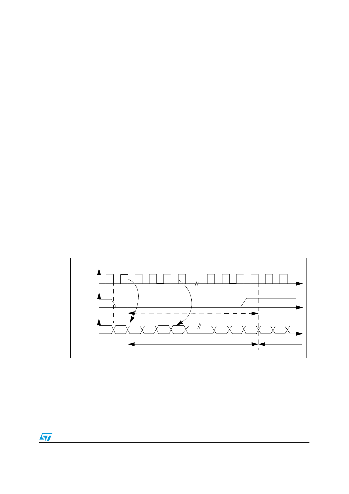
I2S (IC to IC Sound) is an audio data transfer standard using a three-line bus for serial and
synchronous data transmission.
Data are transmitted on the SD line (Serial Data) in Little Endian format (MSB first). Data
length is not limited (usually 16/20/24/32/64 bits). Data are synchronized by the SCK (Serial
Clock) rising or falling edge for the transmitter, and falling edge only for the receiver. Refer to
Figure 1.
Data represent stereo digital sound, so each sample contains two words, the right channel
sample and the left channel sample. Instead of using two data channels, muxing is
performed by transmitting each word in half a sampling period and that allows, by doubling
the sampling rate, to transmit two words per period.
A control signal WS (Word Select) is then used to determine if the word being sent is the
right or the left one. This signal also determines the beginning and the end of the data: there
is no need to fix the data length. Receiver and transmitter data lengths can therefore be
different, as well as the right and left data lengths.
WS is synchronized either on the rising or the falling edge of SCK and precedes the MSB by
one SCK period in order to have enough time for storing and shifting operations.
As in the SPI protocol, there must be a master and a slave. The master controls and
provides the SCK clock and the WS signal, while the slave only sends or receives data. The
master can be the receiver or the transmitter or a third element (Controller). Refer to
Figure 2.
Figure 1. I2S Philips protocol waveforms 16/32-bit
CK
WS
SD
Transmission
MSB
Reception
16-bit or 32-bit
MSB
LSB
Left channel Right channel
3/15
General description AN2682 - Application note
Figure 2. I2S protocol signal description and configuration
SCK
Transmitter Receiver
WS
SD
Transmitter = Master Receiver = Master
Receiver Transmitter
Controller
SCK
Transmitter
WS
SD
Controller = Master
Receiver
SCK
WS
SD
1.2 SPI protocol
The SPI is chosen to implement this solution because its protocol is the most similar to the
I2S protocol.
It uses four pins:
● Two pins (MOSI and MISO) to transmit and receive serial data
● One pin (SCLK) for data clocking (either rising or falling edge modes are available)
● One pin (nSS) to choose between master and slave modes.
When nSS is tied to Gnd, the SPI peripheral functions in Slave mode: it receives the data
clock (SCLK) from the master which controls how and when data are transmitted or
received.
When nSS is tied to Vcc, the SPI peripheral functions in master mode and SCLK is then an
output.
MISO is the Master Input in master mode and the Slave Output in slave mode.
MOSI is the Master Output in master mode and the Slave Input in slave mode.
There are two main differences between the I2S and SPI protocols:
● The I2S clock is continuous while the SPI clock is generated only during word
transmission and is stopped afterwards.
● The data format in SPI protocol is fixed to 16 or 8 bits only, while the data in I2S can
have any length.
Due to these two differences, the SPI peripheral cannot be configured in master mode in
this case. This is due to the fact that in SPI master mode, data are transmitted with a delay
between the words. Besides, many difficulties would arise when other tasks are performed
by the microcontroller. So the solution uses the SPI in slave mode.
4/15
AN2682 - Application note CPLD design
2 CPLD design
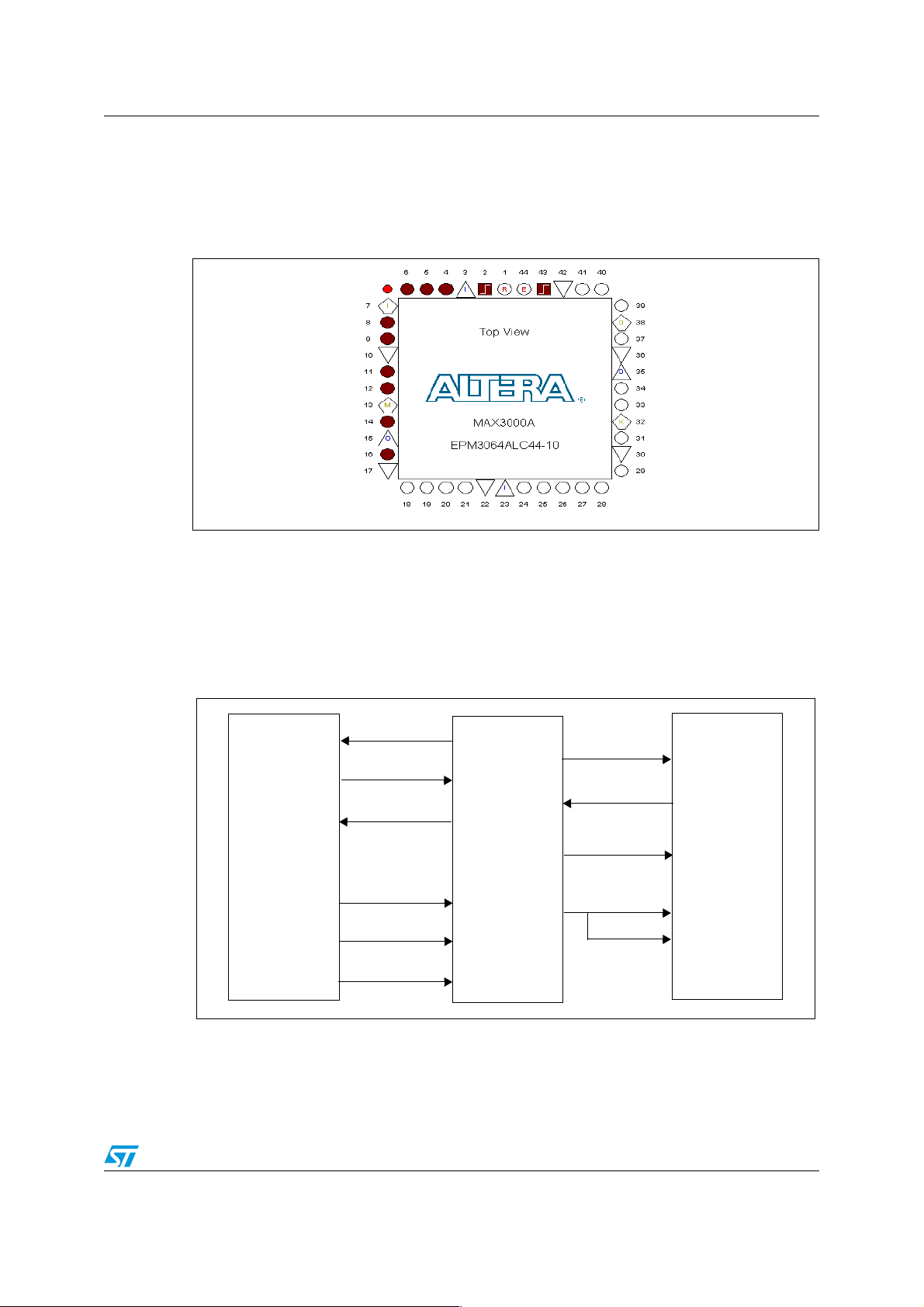
The CLPD design is based on the MAX3000A 32 macrocell device shown in Figure 3.
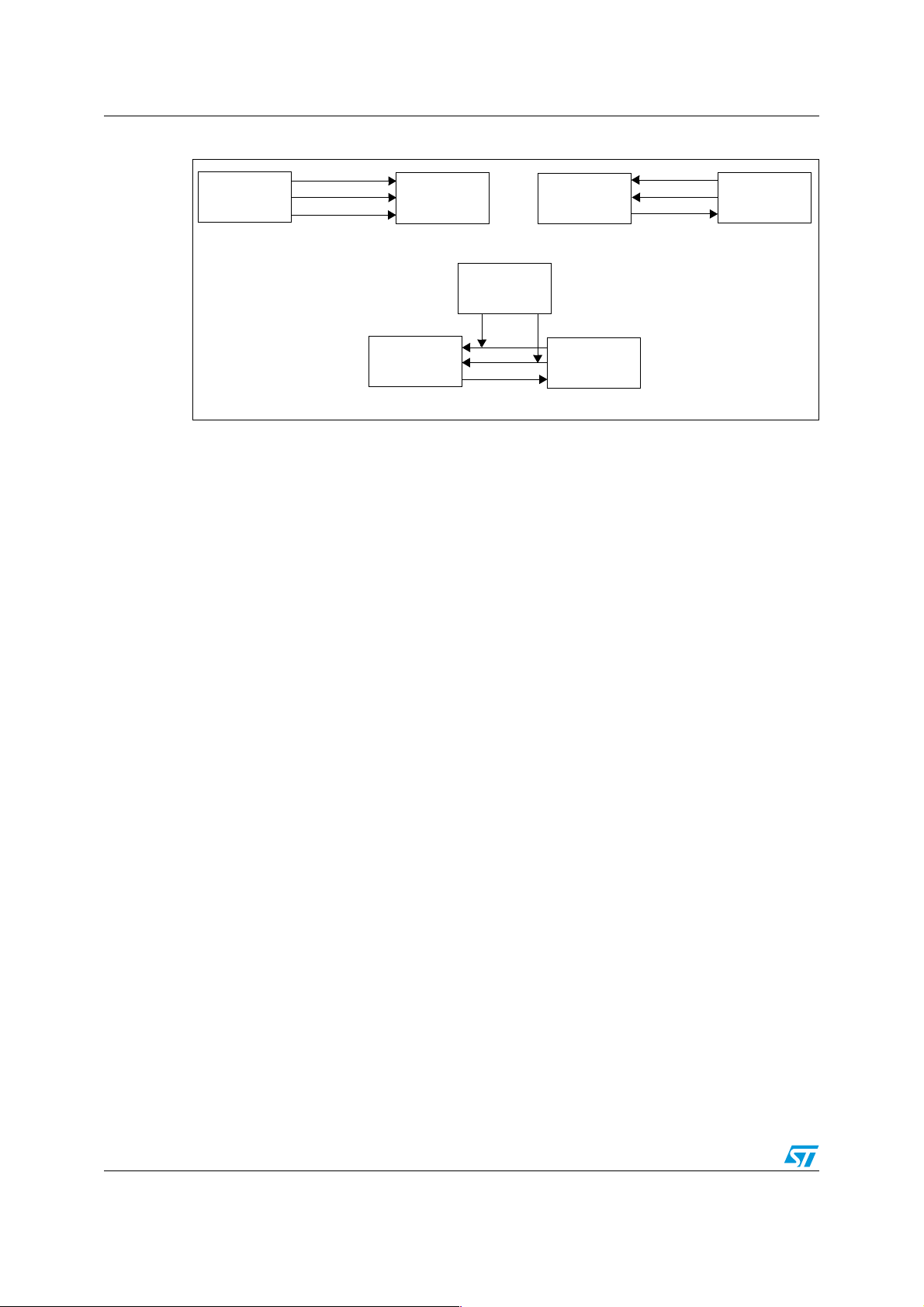
Figure 3. MAX3000A CPLD pin description
The CPLD bridge is intended to function as the master for both SPI and I2S devices. Since
the SPI peripheral is bidirectional, two I2S devices can be connected at once, as long as
they have the same SCK clock (some I2S devices are also bidirectional).
When a single device is interfaced to the microcontroller, the unused direction logic can
simply be ignored and has no effect on the interface. The CPLD bridge connections with the
STR7/9 MCU and the I2S audio device(s) are illustrated in Figure 4.
Figure 4. SPI to I2S CPLD bridge connections
AF
GPIO/AF
GPIO/AF
STR7/9
MCU
PWM OCMPA
GPIO
GPIO
MOSI
MISO
SCLK
CLK
Start
Conf
CPLD
interface
SDo
SDi
SCK
WSo
WSi
Audio
I2S
device(s)
The Conf pin is used only in configuration mode. In communication mode, it can be used for
any other application purpose.
5/15

CPLD design AN2682 - Application note
The I2S signal combination chosen for this solution is:
● Transmitter SD active on SCK falling edge
● Receiver SD active on SCK falling edge
● WS active on SCK falling edge
The CPLD brige functions in two modes:
1. Configuration mode: When the Start signal is low, the interface waits for configuration
parameters. These parameters are transmitted through a three-bit register named
Conf_Reg:
Figure 5. Conf_Reg content
bit 0 bit 1 bit 2
Transmit
Receive
DW
The Transmit and Receive bits activate or disactivate the corresponding directions in or
out of the CPLD interface.
DW (Double Word), when set, enables the support of any data format from 17 to 32 bits
by setting a WS length of 32 bits instead of 16.
The configuration register is set by the MISO line clocked by the falling edge of the Conf
signal while Start is low.
2. Communication mode: This mode is active when the Start signal is high. The
interface generates the SCLK and SCK signals with their associated delays. It also
controls the WS signal as well as the data lengths.
The CPLD implementation is illustrated in Figure 6.
Figure 6. SPI to I2S CPLD bridge internal diagram
CLK
Start
Conf
MISO
CLK
CLK
Start
WSt
Mode select
CLK
Delay control
WS generator
16 bits
32bits
Conf_reg
Tr an s m it
TR enable 1
TR enable 2
DW
Receive
WSt
MISO
Start
DW
Central
block
CLK
SCLK
MOSI
SDo
WSo
SCK
Start
I2S clock control
The solution is synthesized on ALTERA QUARTUSII software using a MAX3000A 32
macrocell device. The implementation is done with 17 macrocells.
The VHDL code implementation is provided with this AN for STR71x and STR750. The
STR750 VHDL code can also be used for the STR91x and STM32 microcontroller.
6/15
SCKi
SDi
WSi

AN2682 - Application note STR711 implementation example
3 STR711 implementation example
3.1 Hardware implemention
The CPLD and STR711 SPI connections are illustrated in Figure 7
Figure 7. MAX3000A and STR711 SPI connections
3.3 V
1
2
3
4
5
6
7
8
JTAG to USB Blaster connector
9
10
TCLK
Gnd
TDO
Vcc
TMS
NC
NC
NC
TDI
Gnd
TCLK
TDI
TDO
TMS
VCCIO
VCCIO
VCCINT
VCCINT
Gnd
Gnd
Gnd
Gnd
Gnd
Gnd
32
7
38
13
15
35
3
23
10
17
22
30
36
42
R
44
E
1
Start
43
CLK
2
MISO
4
MOSI
5
SCLK
6
Conf
8
WSo
9
EPM3064 ALC10-N
11
12
14
16
SDo
SCK
WSi
SDi
Left in HiZ input state
Left in HiZ input state
I2S Audio device
P0.12
OCMPA
MISO
MOSI
SCLK
P0.13
nSS
3
52
53
54
5
40
55
STR711
7/15

STR711 implementation example AN2682 - Application note
3.2 STR711 firmware description
This section describes how to use the SPI to I2S bridge in your application firmware, the
description is based on the source code for STR71x provided with this application note.
First, the STR71x peripherals are initialized:
● The TIM1 timer is configured in PWM mode with a period and duty cycle corresponding
to the user defined CLK frequency.
● The BSPI0 is configured in slave mode, with falling edge clock (CPOL=0, CPHA=1), 16
bit format, 10-word Transmit and Receive FIFO depth, clock divider calculated to
correspond to the user-defined BSPI clock frequency and Transmit FIFO empty
interrupt enabled (or Receive FIFO full interrupt if receive-only mode is active).
● The EIC interrupt controller is configured to enable BSPI interrupt IRQ with the highest
priority.
The STR71x microcontroller performs two main functions:
1. Configuration function: the microcontroller gets the user-defined Conf_Reg register
value from the DEFINE statements, then sets the Start pin low and transmits the three
bits clocked by the Conf falling edge.
2. Communication function: After setting the Start signal high, the microcontroller waits
for an internal interrupt indicating that the transmit FIFO is empty or that the receive
FIFO is full. Then in the interrupt handler, the transmit FIFO is loaded from the audio
file and the receive FIFO is read and loaded in the corresponding file. This whole
operation is done while the last word is being transmitted and received (bidirectional
BSPI shift register). This results in fluent data transfer with no delays or breaks.
8/15

AN2682 - Application note STR711 implementation example
3.2.1 CPU usage
In order to estimate the efficiency of this solution, for integration in different applications, we
can calculate the CPU load relative to the I2S communication. This value determines the
ratio of time dedicated to the I2S task. This value is calculated as follows:
Tc
C
------ -=
T
T is time between the transmission of two words, so:
1
----------------
T
SCLK
16 DW TF×××=
Where DW=1 or 2 depending on the word format (1 to 16 bits or 2 for 17 to 32 bits), and T
is the FIFO size.
Tc is the CPU usage time, obtained (considering a mean instruction length of 3 CPU
cycles), by adding:
● The time required to load the FIFOs (2 x T
● The time needed to save and reload the context (16 + 26 CPU cycles).
● The interrupt code execution time (47 x 3 CPU cycles).
● Other durations need to be added such as the latency between the APB and the AHB
x 3 CPU cycles).
F
buses, the time related to the library operations, the optimization type used...
Determining the exact duration of all these terms is outside the scope of this document
and requires specific and detailed explanations for each case. The intention here is to
give a simplified overview of the performance.
For a 32 MHz MCLK frequency, 16-bit format and 10-word FIFO length, the CPU usage is
therefore:
C = 3.9%
F
9/15

STR711 implementation example AN2682 - Application note
Figure 8. STR71x firmware flowchart
Begin
Initialize peripherals
(BSPI, XTI, TIM, EIC, GPIO...)
Generate CLK
Configuration mode
Set Conf_Reg
Communication mode
End of audio file?
YES
Configuration mode
END
File
File
NO
BSPI Interrupt
TrFIFO empty?
YES
Load TrFIFO (10 words)
Increment File pointer
NO
Tr & Rc mode?
YES
Read RcFIFO (10 words)
Increment File pointer
End of File?
YES
Disable BSPI interrupts
NO
NO
RcFIFO full?
YES
NO
10/15
Clear Flags
END

AN2682 - Application note STR750 implementation example
4 STR750 implementation example
4.1 Hardware implementation
The CPLD and STR750 SSP connections are illustrated in Figure 9.
Figure 9. MAX3000A and STR750 SSP connections
TCLK
TDI
TDO
TMS
VCCIO
3.3 V
1
2
3
4
5
6
7
8
JTAG to USB Blaster connector
9
10
TCLK
Gnd
TDO
Vcc
TMS
NC
NC
NC
TDI
Gnd
VCCIO
VCCINT
VCCINT
Gnd
Gnd
Gnd
Gnd
Gnd
Gnd
32
7
38
13
15
35
3
23
10
EPM3064 ALC10-N
17
22
30
36
42
44
1
43
2
5
8
9
11
12
14
16
R
Left in HiZ input state
Left in HiZ input state
E
Start
CLK
MISO
4
MOSI
SCLK
6
Conf
WSo
SDo
SCK
WSi
SDi
I2S Audio device
P2.18
PWM1
S0.MISO
S0.MOSI
S0.SCLK
P2.19
32
77
76
78
31
81
STR750
4.2 STR750 firmware description
For the STR750, the DMA is used instead of the interrupt method. That makes the software
more simple and, since the DMA automatically transfers the data from peripheral to memory
and from memory to peripheral there is no CPU load.
The STR750 SSP peripheral is configured in SPI Motorola mode.
11/15

STR750 implementation example AN2682 - Application note
First, the STR750 peripherals are initialized:
● The TIM0/PWM timer is configured in PWM mode with a period and duty cycle
corresponding to the user defined CLK frequency.
● The SSP0 is configured in slave mode, rising edge clock (CPOL=1, CPHA=1), 16 bit
format, 8 words Transmit and Receive FIFO depth.
● The DMA is configured to enable SSP Transmit (from memory to peripheral) on
channel 0 and SSP Receive (from peripheral to memory) on channel 1.
The STR75x microcontroller performs two main functions:
1. Configuration function: the microcontroller gets the user-defined Conf_Reg register
value from the DEFINE statements, then sets Start pin low and transmit the three bits
clocked by Conf falling edge.
2. Communication function: After setting the Start signal high, only the DMA is active
and it loads the Transmit FIFO from memory whenever it is half empty and loads the
memory from the Receive FIFO whenever it is half full. The CPU is totally free for any
other application tasks.
Figure 10. STR75x firmware flowchart
Begin
Initialize peripherals
End Of Count
(SSP, TIM0, DMA, GPIO...)
Stop PWM counter
Generate CLK
Clear Flags
Configuration mode
END
Set Conf_Reg
End Of Count
Communication mode
END
In this flowchart, the DMA function is not shown because it works in the background and has
no effect on the CPU. The same flowchart can be used for STR91x.
The STR75x firmware can be easily tailored to any STR91x or STM32 microcontroller.
12/15

AN2682 - Application note Conclusion
5 Conclusion
This application note gives a straightforward and low cost solution for using the STR7xx SPI
peripheral with an audio device (Codec, ADC, DAC, filter...) using I2S protocol via an
external interface consisting of a low cost small CPLD. This solution can be easily tailored to
the STR91x and STM32 microcontrollers.
13/15

Revision history AN2682 - Application note
6 Revision history
Table 1. Document revision history
Date Revision Changes
08-Jan-2008 1 Initial release.
14/15

AN2682 - Application note
Please Read Carefully:
Information in this document is provided solely in connection with ST products. STMicroelectronics NV and its subsidiaries (“ST”) reserve the
right to make changes, corrections, modifications or improvements, to this document, and the products and services described herein at any
time, without notice.
All ST products are sold pursuant to ST’s terms and conditions of sale.
Purchasers are solely responsible for the choice, selection and use of the ST products and services described herein, and ST assumes no
liability whatsoever relating to the choice, selection or use of the ST products and services described herein.
No license, express or implied, by estoppel or otherwise, to any intellectual property rights is granted under this document. If any part of this
document refers to any third party products or services it shall not be deemed a license grant by ST for the use of such third party products
or services, or any intellectual property contained therein or considered as a warranty covering the use in any manner whatsoever of such
third party products or services or any intellectual property contained therein.
UNLESS OTHERWISE SET FORTH IN ST’S TERMS AND CONDITIONS OF SALE ST DISCLAIMS ANY EXPRESS OR IMPLIED
WARRANTY WITH RESPECT TO THE USE AND/OR SALE OF ST PRODUCTS INCLUDING WITHOUT LIMITATION IMPLIED
WARRANTIES OF MERCHANTABILITY, FITNESS FOR A PARTICULAR PURPOSE (AND THEIR EQUIVALENTS UNDER THE LAWS
OF ANY JURISDICTION), OR INFRINGEMENT OF ANY PATENT, COPYRIGHT OR OTHER INTELLECTUAL PROPERTY RIGHT.
UNLESS EXPRESSLY APPROVED IN WRITING BY AN AUTHORIZED ST REPRESENTATIVE, ST PRODUCTS ARE NOT
RECOMMENDED, AUTHORIZED OR WARRANTED FOR USE IN MILITARY, AIR CRAFT, SPACE, LIFE SAVING, OR LIFE SUSTAINING
APPLICATIONS, NOR IN PRODUCTS OR SYSTEMS WHERE FAILURE OR MALFUNCTION MAY RESULT IN PERSONAL INJURY,
DEATH, OR SEVERE PROPERTY OR ENVIRONMENTAL DAMAGE. ST PRODUCTS WHICH ARE NOT SPECIFIED AS "AUTOMOTIVE
GRADE" MAY ONLY BE USED IN AUTOMOTIVE APPLICATIONS AT USER’S OWN RISK.
Resale of ST products with provisions different from the statements and/or technical features set forth in this document shall immediately void
any warranty granted by ST for the ST product or service described herein and shall not create or extend in any manner whatsoever, any
liability of ST.
ST and the ST logo are trademarks or registered trademarks of ST in various countries.
Information in this document supersedes and replaces all information previously supplied.
The ST logo is a registered trademark of STMicroelectronics. All other names are the property of their respective owners.
© 2008 STMicroelectronics - All rights reserved
STMicroelectronics group of companies
Australia - Belgium - Brazil - Canada - China - Czech Republic - Finland - France - Germany - Hong Kong - India - Israel - Italy - Japan -
Malaysia - Malta - Morocco - Singapore - Spain - Sweden - Switzerland - United Kingdom - United States of America
www.st.com
15/15
 Loading...