

AN2681
Application note
ST2S06A33 / ST2S06B
synchronous dual buck converter with reset
Introduction
The ST2S06 is a dual synchronous step-down DC-DC converter optimized for powering
low-voltage digital cores in ODD applications and, generally, used to replace the high
current linear solution when the power dissipation may cause a high heating of the
application environment. It provides up to 0.5 A over an input voltage range of 2.5 V to 5.5 V.
A high switching frequency (1.5 MHz) allows the use of tiny surface-mount components. A
resistor divider to set the output voltage value, an inductor and two capacitors are required
for every channel. In addition, a low output ripple is guaranteed by the current mode PWM
topology and by the use of low ESR surface-mount ceramic capacitors.
The device is thermal protected and current limited to prevent damage due to accidental
short-circuit.
The family is available in the QFN12L (4x4 mm) package.
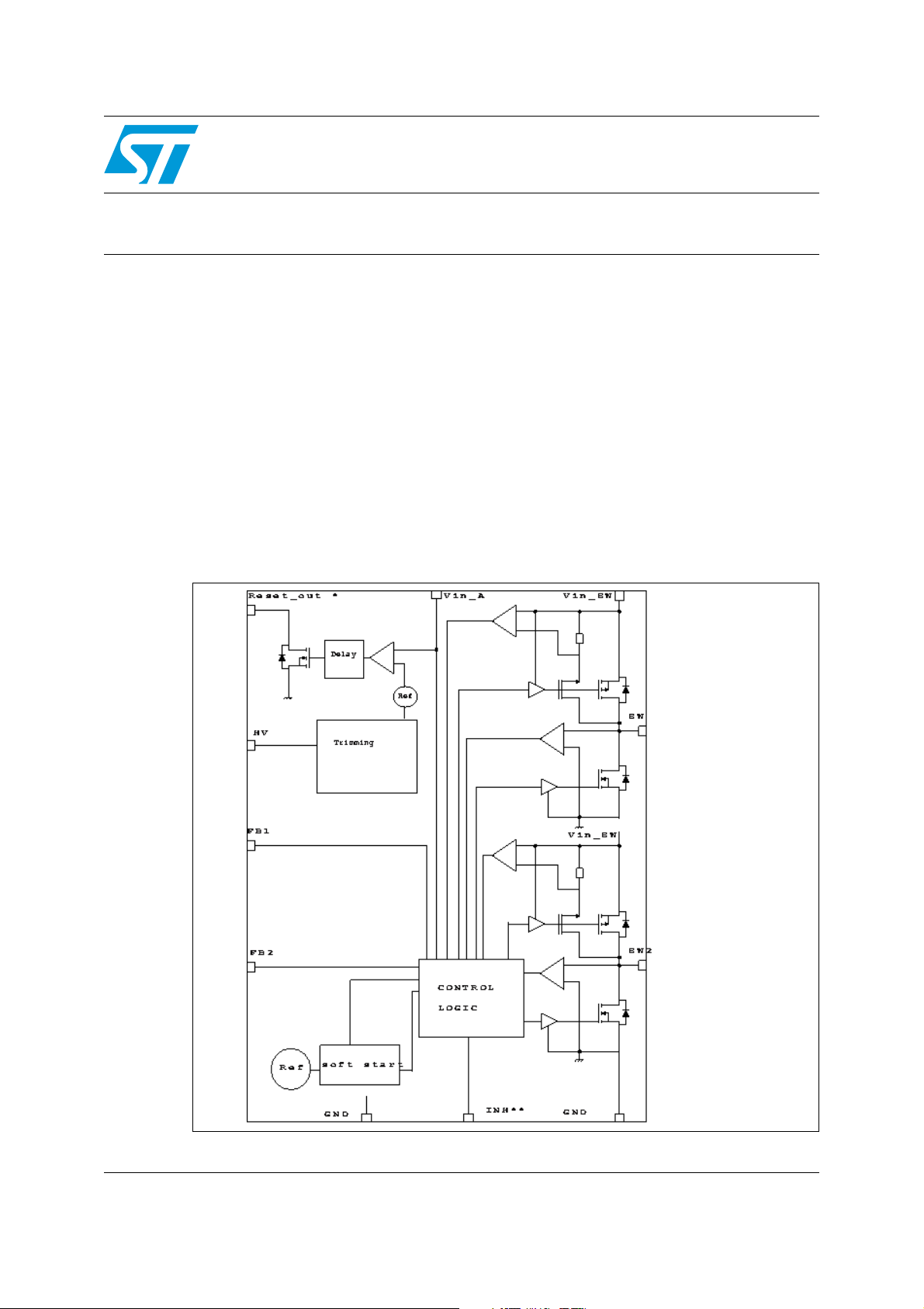
Figure 1. ST2S06 - simplified schematic
* Only ST2S06A/D
** Only ST2S06B
September 2008 Rev 2 1/23
www.st.com

Contents AN2681
Contents
1 ST2S06 description . . . . . . . . . . . . . . . . . . . . . . . . . . . . . . . . . . . . . . . . . . 4
1.1 Inhibit function (ST2S06B only) . . . . . . . . . . . . . . . . . . . . . . . . . . . . . . . . . 7
1.2 Reset function (ST2S06A and ST2S06D only) . . . . . . . . . . . . . . . . . . . . . 7
1.3 Short-circuit protection . . . . . . . . . . . . . . . . . . . . . . . . . . . . . . . . . . . . . . . 10
2 Selecting components for applications . . . . . . . . . . . . . . . . . . . . . . . . 11
2.1 Output voltage selection . . . . . . . . . . . . . . . . . . . . . . . . . . . . . . . . . . . . . . 11
2.2 Input capacitor . . . . . . . . . . . . . . . . . . . . . . . . . . . . . . . . . . . . . . . . . . . . . 12
2.3 Output capacitor . . . . . . . . . . . . . . . . . . . . . . . . . . . . . . . . . . . . . . . . . . . . 13
2.4 Inductor . . . . . . . . . . . . . . . . . . . . . . . . . . . . . . . . . . . . . . . . . . . . . . . . . . 13
2.5 Layout considerations . . . . . . . . . . . . . . . . . . . . . . . . . . . . . . . . . . . . . . . . 14
3 Thermal considerations . . . . . . . . . . . . . . . . . . . . . . . . . . . . . . . . . . . . . 15
4 Demonstration board usage recommendation . . . . . . . . . . . . . . . . . . . 16
4.1 External component selection . . . . . . . . . . . . . . . . . . . . . . . . . . . . . . . . . 18
4.1.1 Capacitors selection . . . . . . . . . . . . . . . . . . . . . . . . . . . . . . . . . . . . . . . 19
4.1.2 Inductor selection . . . . . . . . . . . . . . . . . . . . . . . . . . . . . . . . . . . . . . . . . . 19
5 Bill of materials . . . . . . . . . . . . . . . . . . . . . . . . . . . . . . . . . . . . . . . . . . . . 21
6 Recommended footprint . . . . . . . . . . . . . . . . . . . . . . . . . . . . . . . . . . . . . 22
7 Revision history . . . . . . . . . . . . . . . . . . . . . . . . . . . . . . . . . . . . . . . . . . . 22
2/23

AN2681 List of figures
List of figures
Figure 1. ST2S06 - simplified schematic . . . . . . . . . . . . . . . . . . . . . . . . . . . . . . . . . . . . . . . . . . . . . . . 1
Figure 2. Inductor current at light load . . . . . . . . . . . . . . . . . . . . . . . . . . . . . . . . . . . . . . . . . . . . . . . . . 4
Figure 3. Output voltage ripple at light load . . . . . . . . . . . . . . . . . . . . . . . . . . . . . . . . . . . . . . . . . . . . . 5
Figure 4. Inductor current in PWM . . . . . . . . . . . . . . . . . . . . . . . . . . . . . . . . . . . . . . . . . . . . . . . . . . . . 5
Figure 5. Output voltage ripple in PWM . . . . . . . . . . . . . . . . . . . . . . . . . . . . . . . . . . . . . . . . . . . . . . . . 6
Figure 6. Inrush current . . . . . . . . . . . . . . . . . . . . . . . . . . . . . . . . . . . . . . . . . . . . . . . . . . . . . . . . . . . . 6
Figure 7. ST2S06B - inhibit voltage vs. temperature . . . . . . . . . . . . . . . . . . . . . . . . . . . . . . . . . . . . . . 7
Figure 8. ST2S06A\D - reset block diagram . . . . . . . . . . . . . . . . . . . . . . . . . . . . . . . . . . . . . . . . . . . . 8
Figure 9. ST2S06A\D - reset function . . . . . . . . . . . . . . . . . . . . . . . . . . . . . . . . . . . . . . . . . . . . . . . . . 8
Figure 10. Pull-up resistor . . . . . . . . . . . . . . . . . . . . . . . . . . . . . . . . . . . . . . . . . . . . . . . . . . . . . . . . . . . 9
Figure 11. ST2S06D - delay time. . . . . . . . . . . . . . . . . . . . . . . . . . . . . . . . . . . . . . . . . . . . . . . . . . . . . . 9
Figure 12. Reset_in threshold vs. temperature . . . . . . . . . . . . . . . . . . . . . . . . . . . . . . . . . . . . . . . . . . . 9
Figure 13. TDEL vs. temperature. . . . . . . . . . . . . . . . . . . . . . . . . . . . . . . . . . . . . . . . . . . . . . . . . . . . . 10
Figure 14. Typical application schematic . . . . . . . . . . . . . . . . . . . . . . . . . . . . . . . . . . . . . . . . . . . . . . . 11
Figure 15. Feedback voltage vs. temperature . . . . . . . . . . . . . . . . . . . . . . . . . . . . . . . . . . . . . . . . . . . 12
Figure 16. Layout considerations . . . . . . . . . . . . . . . . . . . . . . . . . . . . . . . . . . . . . . . . . . . . . . . . . . . . . 14
Figure 17. Demonstration board layout . . . . . . . . . . . . . . . . . . . . . . . . . . . . . . . . . . . . . . . . . . . . . . . . 16
Figure 18. Demonstration board - top layer . . . . . . . . . . . . . . . . . . . . . . . . . . . . . . . . . . . . . . . . . . . . . 17
Figure 19. Demonstration board - bottom layer . . . . . . . . . . . . . . . . . . . . . . . . . . . . . . . . . . . . . . . . . . 17
Figure 20. Demonstration board schematic for ST2S06A\D . . . . . . . . . . . . . . . . . . . . . . . . . . . . . . . . 18
Figure 21. Demonstration board schematic for ST2S06B . . . . . . . . . . . . . . . . . . . . . . . . . . . . . . . . . . 18
Figure 22. Efficiency vs. output current . . . . . . . . . . . . . . . . . . . . . . . . . . . . . . . . . . . . . . . . . . . . . . . . 19
Figure 23. Efficiency vs. inductor . . . . . . . . . . . . . . . . . . . . . . . . . . . . . . . . . . . . . . . . . . . . . . . . . . . . . 20
Figure 24. Efficiency vs. output voltage . . . . . . . . . . . . . . . . . . . . . . . . . . . . . . . . . . . . . . . . . . . . . . . . 20
Figure 25. QFN12L (4x4 mm) footprint recommended data . . . . . . . . . . . . . . . . . . . . . . . . . . . . . . . . 22
3/23
ST2S06 description AN2681
1 ST2S06 description
The ST2S06 is a dual adjustable current mode PWM synchronous step-down DC/DC
converter with an internal 0.5 A power switch. It is a complete 0.5 A dual switching regulator
with internal compensation that eliminates the need for additional components.
The device is available in three versions, the ST2S06A and ST2S06D with a reset function
and the ST2S06B with an inhibit function.
The ST2S06 family operates with typically 1.5 MHz fixed frequency.
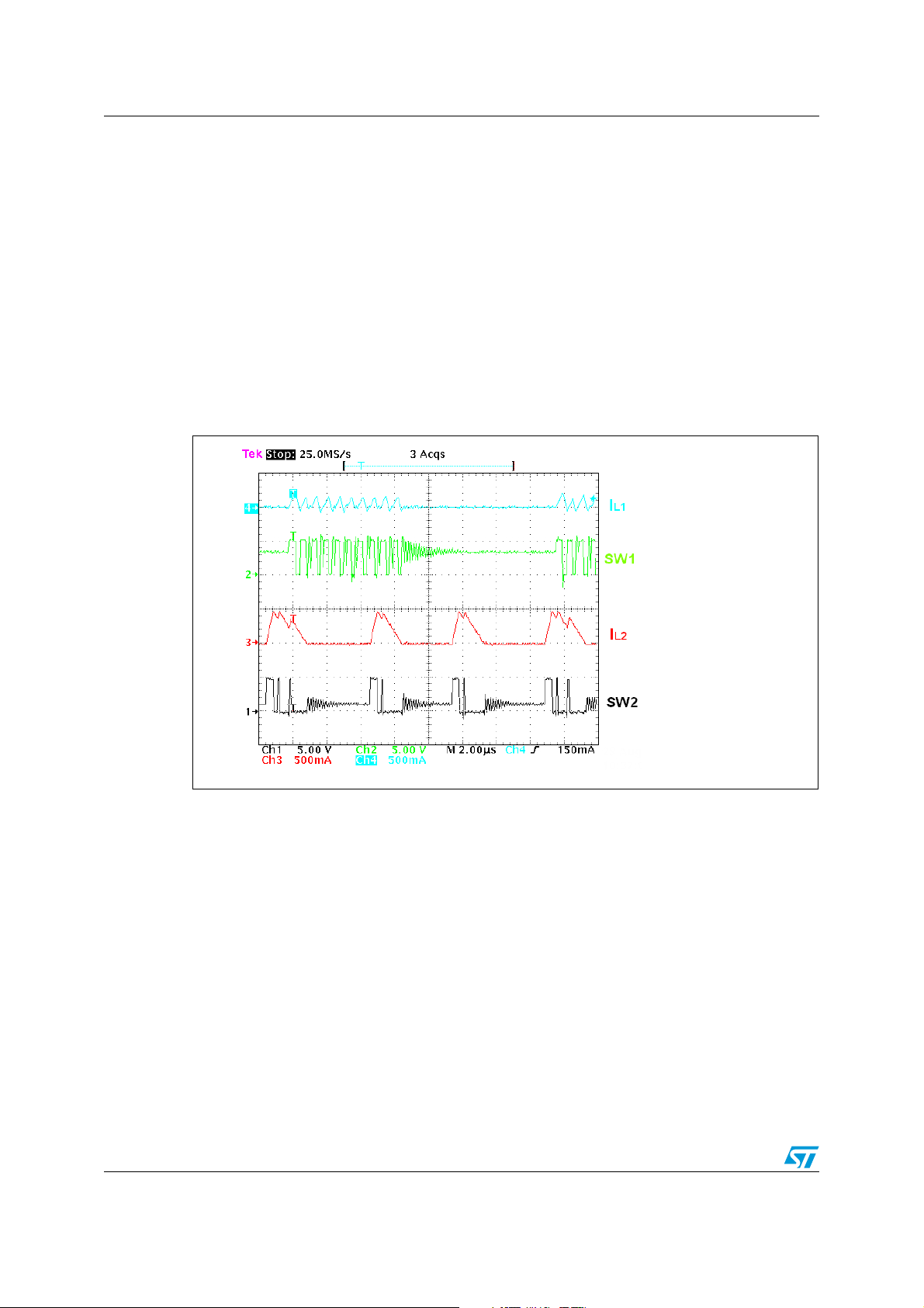
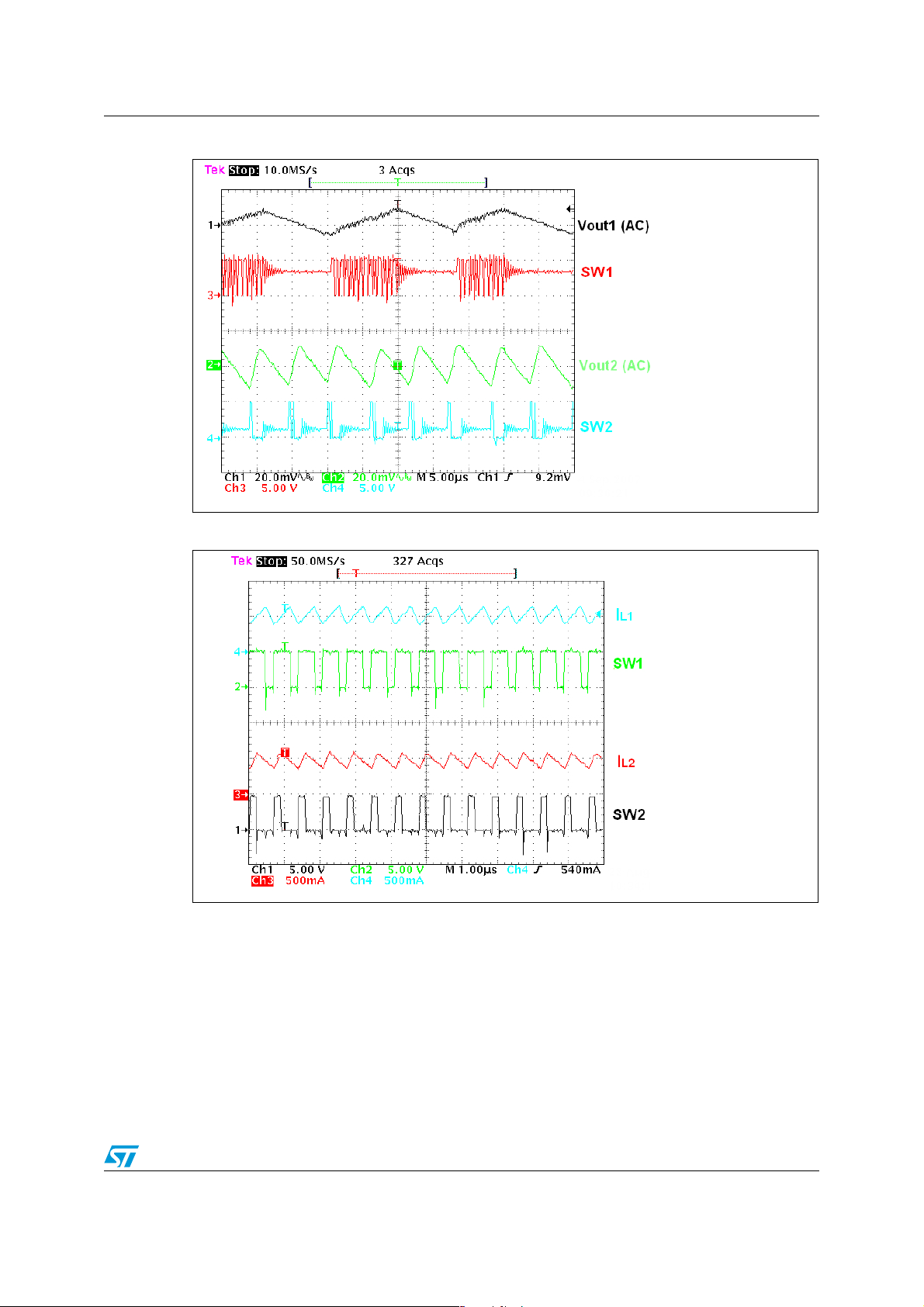
To maintain good efficiency at both channels, the devices operate in power-save mode at
light load (Figure 2 and 3). When the load increases it automatically switches to PWM (pulse
width modulation) mode in order to reduce the output voltage ripple (Figure 4 and 5).
Figure 2. Inductor current at light load
Vin=5 V
V
=3.3 V
out1
V
=1.2 V
out2
=20 mA
I
out1
I
=100 mA
out2
4/23
AN2681 ST2S06 description
Figure 3. Output voltage ripple at light load
=5 V
V
in
V
=3.3 V
out1
V
=1.2 V
out2
R
R
LOAD1
LOAD2
=150 Ω
=15 Ω
Figure 4. Inductor current in PWM
Vin=5 V
V
=3.3 V
out1
V
=1.2 V
out2
I
=500 mA
out1
I
=500 mA
out2
5/23
ST2S06 description AN2681
Figure 5. Output voltage ripple in PWM
Vin=5 V
V
=3.3 V
out1
V
=1.2 V
out2
R
R
LOAD1
LOAD2
=10 Ω
=3.3 Ω
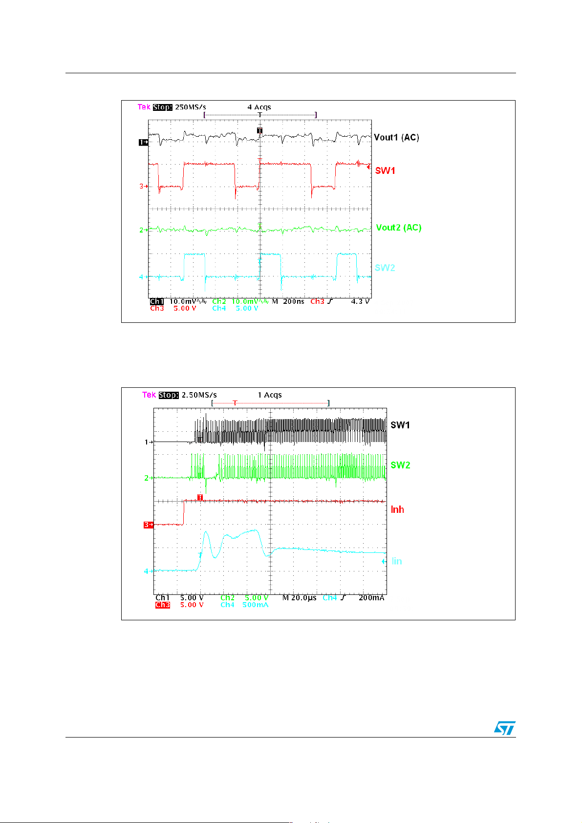
To clamp the error amplifier reference voltage, a Soft Start control block generating a voltage
ramp is implemented. When switching on the power supply, it allows controlling the inrush
current value.
Figure 6. Inrush current
Vin=5 V
V
=3.3 V
out1
V
=1.2 V
out2
R
R
LOAD1
LOAD2
=10 Ω
=3.3 Ω
Other protection circuits in the device are the thermal shutdown block which turns off the
regulator when the junction temperature exceeds 150 °C (typ.) and the cycle-by-cycle
current limiting that provides protection against shorted outputs.
Operation of the device requires few components: two inductors, three capacitors and two
resistor dividers. The inductors chosen must be capable of not saturating at the peak current
level. The value of the inductors should be selected keeping in mind that a large inductor
value increases the efficiency at low output current and reduces output voltage ripple, while
6/23
AN2681 ST2S06 description
a smaller inductor can be chosen when it is important to reduce the package size and the
total application cost.
Finally, the ST2S06 family has been designed to work properly with X5R or X7R SMD
ceramic capacitors both at input and at output. These capacitors, thanks to their very low
series resistance (ESR), minimize the output voltage ripple. Other low ESR capacitors can
be used according to the need of the application without compromising the correct
functioning of the device.
Due to the high switching frequency and peak current, it is important to optimize the
application environment by reducing the length of the PCB traces and placing all external
components near the device.
1.1 Inhibit function (ST2S06B only)
The ST2S06B features an Inhibit function (pin 10). When the Inh voltage is higher than
1.3 V the device is On and if it is lower than 0.4 V the device is OFF. In shutdown mode
consumption is lower than 1 µA.
The Inh pin does not have an internal pull-up which means that you cannot leave the inhibit
floating.
If the inhibit function is not used, the Inh pin must be connected to V
Figure 7. ST2S06B - inhibit voltage vs. temperature
1.5
1.3
1.1
0.9
Vinh (V)
0.7
Vin=5V, Iout1,2=100mA
0.5
-50 -25 0 25 50 75 100 125
T [C°]
ON OFF
1.2 Reset function (ST2S06A and ST2S06D only)
Most ODD applications require a flag showing that the input voltage is in the correct range.
.
in
7/23

ST2S06 description AN2681
Figure 8. ST2S06A\D - reset block diagram
Vin_A
Reset_out
Delay
Ref
Figure 8 shows the simplified reset block diagram. A comparator senses the input voltage.
When it is higher than VTL (4.2 V for ST2S06A or 3.7 V for ST2S06D), the reset_out pin
goes to high impedance. If it is below VTH (4.6 V for ST2S06A or 4.55 V max for ST2S06D),
the reset_out pin goes to low impedance with a delay of 100 ms (typ.) for ST2S06A or 65 ms
(typ.) for ST2S06D (see Figure 9 and 11).
Figure 9. ST2S06A\D - reset function
V
V
TH
V
V
IN
IN
Reset
Reset
TH
t
t
DEL
DEL
V
V
TL
TL
The use of the Reset function requires an external pull-up resistor which must be connected
between reset_out pin and V
range of 100 kΩ to 1 MΩ
or V
in
. We suggest using a pull-up resistor for reset in the
out
. If the reset function is not used, the reset_out pin must remain
floating on the board.
In the application board (Figure 10), Rpi is used to pull up the reset_out pin to V
to pull up the reset_out pin to V
or V
.
out
. Of course the reset_out pin can be connected only to Vin
out1
and Rpo
in
8/23

AN2681 ST2S06 description
Figure 10. Pull-up resistor
Figure 11. ST2S06D - delay time
Figure 12. Reset_in threshold vs. temperature
4.7
4.5
4.3
4.1
Vres (V)
3.9
3.7
3.5
-50 -25 0 25 50 75 100 125
T [C°]
Vin=3.6 V to 5 V
Rpo=120 kΩ
Falling ST2S06A
Rising ST2S06A
Falling ST2S06D
Rising ST2S06D
9/23

ST2S06 description AN2681
Figure 13. T
vs. temperature
DEL
100
95
90
85
80
(ms)
75
DEL
70
T
65
60
55
50
-50 -25 0 25 50 75 100 125
1.3 Short-circuit protection
In overcurrent protection mode, when the peak current reaches the current limit, the device
reduces T
and, in most of the applications, this is enough to limit the current to I
In case of heavy short-circuit at the output (V
conditions (V
reach values higher than I
during the ON and OFF phases:
to its minimum value. In these conditions, the duty cycle is strongly reduced
on
value and parasitic effect of external components), the current peak could
in
. This can be understood considering the inductor current ripple
lim
ST2S06A
ST2S06D
T [C°]
.
lim
=0 V) and depending on the application
out
Equation 1
ON phase
V
inVout
---------------------------------------------------------- -
IL∆
DCRLI⋅––()
L
⋅=
T
on
Equation 2
∆
I
L
Where V
OFF phase
is the voltage drop across the internal NMOS and DCRL is the series resistance
D
of the inductor. In short-circuit conditions V
V
DVout
---------------------------------------------------------- -
is negligible. So, during T
out
DCRLI⋅++()
L
⋅=
T
off
, the voltage
off
applied to the inductor is very small and it can be that the current ripple in this phase does
not compensate for the current ripple during T
measured through the inductor with V
= 0 V (short-circuit) and Vin=V
out
. The maximum current peak can be easily
on
. In case the
inmax
application has to sustain the short-circuit condition for a long time, the external components
(mainly inductor) must be selected based on this value.
10/23

AN2681 Selecting components for applications
2 Selecting components for applications
This section provides information to assist in the selection of the most appropriate
components for your applications.
Figure 14 shows the typical application schematic.
Figure 14. Typical application schematic
* ST2S06B
** ST2S06A/D
2.1 Output voltage selection
The output voltage can be adjusted from 0.8 V up to 85% of input voltage value by
connecting a resistor divider between the output and the V
You must choose the resistor divider according to the following equation:
Equation 3
V
outVFB
Figure 13 shows the feedback voltage versus temperature.
We suggest using a resistor with a value in the range of 10 kΩ to 50 kΩ. Lower values are
suitable as well, but will increase current consumption. Be aware that the duty cycle must be
kept below 85% at all application conditions, so that:
Equation 4
D
MAX
R
1
------ -+=
R
2
+
outVF
–
with VFB=0.8 V
1
V
-----------------------------------
V
inMINVSW
pin.
FB
0.85<=
where V
is the voltage drop across the internal NMOS, and VSW represents the voltage
F
drop across the internal PMOS.
11/23

Selecting components for applications AN2681
For output voltages close to the feedback voltage, we suggest adding a very small capacitor
in parallel to R1 in the range of 10 pF. Or, as an alternative, we suggest increasing the
current in the resistor divider by decreasing the R1 and R2 value.
Figure 15. Feedback voltage vs. temperature
0.84
0.83
0.82
0.81
0.8
Vfb [V]
0.79
0.78
0.77
0.76
Vin=5V, Iout1,2=No load
-50 -25 0 25 50 75 100 125
TEMPERATURE [°C]
Vfb1 Vfb2
2.2 Input capacitor
The input capacitor must be able to support the maximum input operating voltage and the
maximum RMS input current.
Since step-down converters draw current from the input impulses, the input current is
squared and the height of each pulse is equal to the output current. The input capacitor has
to absorb all this switching current that can be up to one half of the load current (worst case,
with duty cycle of 50%).
For this reason, the quality of these capacitors has to be very high to minimize its power
dissipation generated by the internal ESR, thus improving the system reliability and
efficiency.
The critical parameter is usually the RMS current rating, which must be higher than the RMS
input current. The maximum RMS input current (flowing through the input capacitor) is:
Equation 5
Where η is the expected system efficiency, D is the duty cycle, and I
current. This function reaches its maximum value at D = 0.5 and the equivalent RMS current
is equal to I
The maximum and minimum duty cycles are:
divided by 2 (considering η = 1).
out
I
RMSIout
2D2⋅
D
-------------- -–
η
2
D
------ -+⋅=
η
the output DC
out
Equation 6
D
MAX
12/23
V
+
outVF
-----------------------------------=
V
–
inMINVSW

AN2681 Selecting components for applications
Equation 7
V
+
outVF
MIN
-------------------------------------=
V
–
inMAXVSW
D
Where V
it is the voltage drop across the internal NMOS and VSW the voltage drop across
F
the internal PMOS. Considering the range D
I
flowing through the input capacitor.
RMS
The use of ceramic capacitors with voltage ratings in the range of 1.5 times the maximum
output voltage is recommended.
2.3 Output capacitor
The output capacitor is very important to satisfy the output voltage ripple requirement. Using
a small inductor value is useful to reduce the size of the coil, but increases the current ripple.
So, to reduce the output voltage ripple a low ESR capacitor is required. The output voltage
ripple (V
OUT_RIPPLE
), in continuous mode, is:
Equation 8
V
outRIPPLE
-
where ∆I is the ripple current and F
The use of ceramic capacitors with voltage ratings in the range of 1.5 times the maximum
output voltage is recommended.
2.4 Inductor
to D
MIN
⎛⎞
⋅=
I∆ ESR
⎝⎠
is the switching frequency.
SW
it is possible to determine the max
MAX
1
-----------------------------------+
⋅⋅
8C
outFSW
The inductor value is very important because it fixes the ripple current flowing through the
output capacitor. The ripple current is usually fixed at 20-40% of I
with I
out_max
= 0.5 A. The inductor value is approximately obtained by the following formula:
out_max
, that is 0.1-0.2 A
Equation 9
VinV
–
out
where T
-------------------------
L
is the ON time of the internal switch, given by D · T. The peak current through the
on
T
⋅=
I∆
on
inductor is given by:
Equation 10
I
PKIout
I∆
---- -+=
2
And it can be seen that if the inductor value decreases, the peak current (that has to be
lower than the current limit of the device) increases. So, for fixed peak current protection, a
higher value of the inductor permits a higher value for the output current.
13/23

Selecting components for applications AN2681
2.5 Layout considerations
Due to the high switching frequency and peak current, the layout is an important design step
for all switching power supplies. If the layout is not carefully done, important parameters
such as efficiency and output voltage ripple could be compromised.
Short, wide traces must be implemented for main current and for power ground paths as
shown in bold in Figure 16. The input capacitors must be placed as close as possible to the
device pins as well as the inductors and output capacitors.
A common ground node minimizes ground noise, as shown in Figure 16.
HV pin must be floating or connected to GND and the exposed pad of the package must be
connected to GND.
Figure 16. Layout considerations
* ST2S06B
** ST2S06A/D
14/23

AN2681 Thermal considerations
3 Thermal considerations
The dissipated power of the device is determined by three different factors:
● Switch losses due to the nonnegligible R
Equation 11
P
ONP
R
-
DS on()P
and
. These are equal to:
DS(on)
2
I
D⋅⋅=
out
-
Equation 12
P
ONN
-
R
DS on()N
2
I
1D–()⋅⋅=
out
-
where D is the duty cycle of the application.
Note: The duty cycle is theoretically given by the ratio between V
higher than this value in order to compensate the losses of the overall application. Due to
this reason, the switch losses related to the R
● On and Off switching losses. These are given by the following relationship:
increase compared to the ideal case.
DS(on)
Equation 13
TonT
+()
off
F
2
SWVinIoutTSWFSW
where T
ON
and T
P
SWVinIout
are the overlap times of the voltage across the power switch and the
OFF
----------------------------- -
current flowing into it during the turn-on and turn-off phases. TSW is the equivalent
switching time.
● Quiescent current losses:
Equation 14
where I
is the quiescent current.
Q
P
QVinIQ
⋅=
The overall losses are:
and Vin, but in practice is quite
out
⋅⋅ ⋅=⋅⋅ ⋅=
Equation 15
For channel 1
P
CH1
Equation 16
For channel 2
P
CH2
Equation 17
R
DS on()P1
-
R
DS on()P2
-
I
I
2
2
D1R
out1
out2
DS on()N1
-
D2R
DS on()N2
-
P
TOTPCH1PCH2VinIQ
I
I
2
out1
2
out2
1D
–()VinI
1
1D
–()VinI
2
⋅++=
⋅⋅ ⋅+⋅⋅+⋅⋅=
out1TSW1FSW1
⋅⋅ ⋅+⋅⋅+⋅⋅=
out2TSW2FSW2
15/23

Demonstration board usage recommendation AN2681
The junction temperature of device is:
Equation 18
TJTARth
⋅+=
JA–PTOT
where T
is the ambient temperature and Rth
A
is the thermal resistance junction to
J-A
ambient.
4 Demonstration board usage recommendation
The demonstration board shown in Figure 17 is provided with a Kelvin connection which
means that for each pin there are two lines available, one used to supply or sink current and
the other one used to perform the needed measurement.
Figure 17. Demonstration board layout
GND Force
Vin Sense
Vin Force Inhibit
Reset Out
Vout2 Sense
Vout2 Force GND Sense
16/23
GND Sense
Vout1 Sense
Vout1 Force

AN2681 Demonstration board usage recommendation
Figure 18. Demonstration board - top layer
Figure 19. Demonstration board - bottom layer
The board has one inhibit pin available which is located on the top side of the board. This pin
can be used to supply the inhibit pin with an external voltage higher than 1.3 V to turn on, or
lower than 0.4 V to turn off the device.
17/23

Demonstration board usage recommendation AN2681
4.1 External component selection
Figure 19 and 20 show the demonstration board schematic.
Figure 20. Demonstration board schematic for ST2S06A\D
Figure 21. Demonstration board schematic for ST2S06B
In order to obtain the needed output voltage, the resistor divider must be selected in
accordance with the following formula:
Equation 19
V
OUT1 2,
with V
FB1,2
= 0.8 V
Table 1. Recommended resistor divider
V
OUT1,2
1.2 V 27 kΩ 47 kΩ
3.3 V 47 kΩ 15 kΩ
18/23
V
R
FB1 2,
1,3
R
13,
1
----------- -+=
R
24,
R
2,4

AN2681 Demonstration board usage recommendation
The resistors dividers in Ta bl e 1 are a good compromise in terms of current consumption
and minimum output voltage.
Note: If ST2S06A33 or ST2S06D33 are mounted in the demonstration board, R1 is replaced with
a short-circuit and R2 is not used.
4.1.1 Capacitors selection
It is possible to use any X5R or X7R ceramic capacitor
● Ci_A = Ci_SW = 4.7 µF (ceramic) or higher.
● Co1 = Co2 = 22 µF (ceramic) or higher. It is possible to put several capacitors in parallel
in order to reduce the equivalent series resistance and improve the ripple present in the
output voltage.
4.1.2 Inductor selection
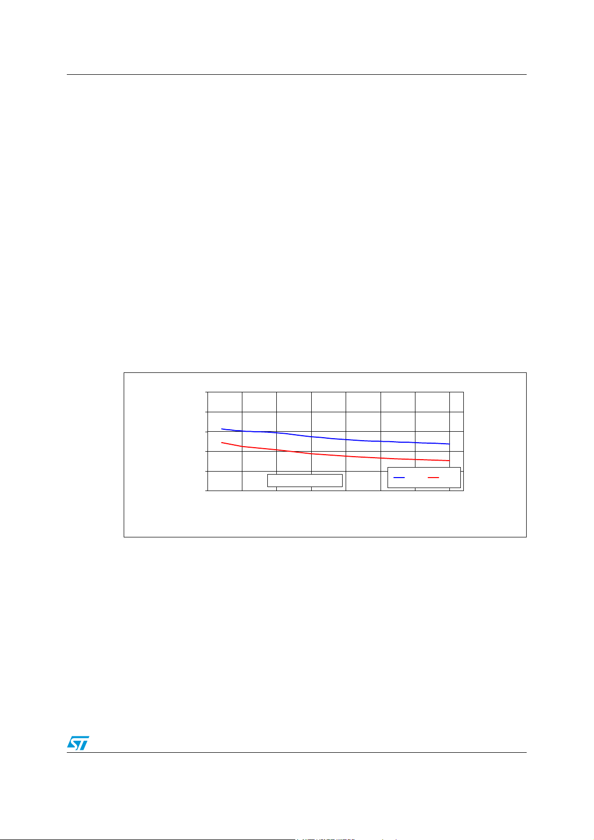
Due to the high frequency (1.5 MHz) it is possible to use very small inductors values. In our
board the device was tested with inductors in the range of 1 µH to 10 µH, with very good
efficiency performances (see below plot in Figure 22).
As the device is able to provide an operative output current of 0.5 A, the use of inductors
capable of managing at least 1.5 A is strongly recommended.
Figure 22. Efficiency vs. output current
100
90
80
70
60
50
40
Efficiency [%]
30
20
10
0
0 50 100 150 200 250 300 350 400 450 500
Vin=5V, L1=L2=3.3µH, Ci_A =
Ci_SW=4.7µF, Co1=Co2=22µF
Vout=1.2V
Vout=2.5V
Vout=3.3V
Iou t [mA]
19/23

Demonstration board usage recommendation AN2681
Figure 23. Efficiency vs. inductor
100
90
80
70
60
Efficiency [%]
50
40
Vin=5V, Vout=3.3V, Ci_A = Ci_SW
=4.7µF, Co1=Co2=22µF
Iout=100mA
Iout=300mA
Iout=500mA
30
0246810
L [µH]
Figure 24. Efficiency vs. output voltage
100
95
90
85
80
75
70
Efficiency [%]
65
60
Vin=5V, L1=L2=3.3µH, Ci_A =
Ci_SW =4.7µF, Co1=Co2=22µF
Iout=300mA
Iout=500mA
55
50
0.511.522.533.54
Vout [V]
Note: All efficiencies are relative to one channel, the other channel is at no-load.
20/23

AN2681 Bill of materials
5 Bill of materials
Table 2. BOM with most common components
Name Value Material Manufacturer P/N
Ci_A 4.7 µF
Ci_SW 4.7 µF
Co1 22 µF
Co2 22 µF
L1 3.3 µH
L2 3.3 µH
Rpi/Rpo 120 kΩ
Ceramic Murata GRM21BR61E475KA12B
Ceramic TDK C3216X7R1C475K
Ceramic Murata GRM21BR61E475KA12B
Ceramic TDK C3216X7R1C475K
Ceramic Murata GRM32ER61E226KE15B
Ceramic TDK C3225X7R1C226M
Ceramic Murata GRM32ER61E226KE15B
Ceramic TDK C3225X7R1C226M
TDK RLF7030T-3R3M4R1
Murata LQH66SN3R3M03L
Coiltronics DR73-3R3
TDK RLF7030T-3R3M4R1
Murata LQH66SN3R3M03L
Coiltronics DR73-3R3
21/23

Recommended footprint AN2681
6 Recommended footprint
Figure 25. QFN12L (4x4 mm) footprint recommended data
7 Revision history
Table 3. Document revision history
Date Revision Changes
08-Jan-2008 1 Initial release
15-Sep-2008 2 Changed: Figure 22, 24
22/23

AN2681
Please Read Carefully:
Information in this document is provided solely in connection with ST products. STMicroelectronics NV and its subsidiaries (“ST”) reserve the
right to make changes, corrections, modifications or improvements, to this document, and the products and services described herein at any
time, without notice.
All ST products are sold pursuant to ST’s terms and conditions of sale.
Purchasers are solely responsible for the choice, selection and use of the ST products and services described herein, and ST assumes no
liability whatsoever relating to the choice, selection or use of the ST products and services described herein.
No license, express or implied, by estoppel or otherwise, to any intellectual property rights is granted under this document. If any part of this
document refers to any third party products or services it shall not be deemed a license grant by ST for the use of such third party products
or services, or any intellectual property contained therein or considered as a warranty covering the use in any manner whatsoever of such
third party products or services or any intellectual property contained therein.
UNLESS OTHERWISE SET FORTH IN ST’S TERMS AND CONDITIONS OF SALE ST DISCLAIMS ANY EXPRESS OR IMPLIED
WARRANTY WITH RESPECT TO THE USE AND/OR SALE OF ST PRODUCTS INCLUDING WITHOUT LIMITATION IMPLIED
WARRANTIES OF MERCHANTABILITY, FITNESS FOR A PARTICULAR PURPOSE (AND THEIR EQUIVALENTS UNDER THE LAWS
OF ANY JURISDICTION), OR INFRINGEMENT OF ANY PATENT, COPYRIGHT OR OTHER INTELLECTUAL PROPERTY RIGHT.
UNLESS EXPRESSLY APPROVED IN WRITING BY AN AUTHORIZED ST REPRESENTATIVE, ST PRODUCTS ARE NOT
RECOMMENDED, AUTHORIZED OR WARRANTED FOR USE IN MILITARY, AIR CRAFT, SPACE, LIFE SAVING, OR LIFE SUSTAINING
APPLICATIONS, NOR IN PRODUCTS OR SYSTEMS WHERE FAILURE OR MALFUNCTION MAY RESULT IN PERSONAL INJURY,
DEATH, OR SEVERE PROPERTY OR ENVIRONMENTAL DAMAGE. ST PRODUCTS WHICH ARE NOT SPECIFIED AS "AUTOMOTIVE
GRADE" MAY ONLY BE USED IN AUTOMOTIVE APPLICATIONS AT USER’S OWN RISK.
Resale of ST products with provisions different from the statements and/or technical features set forth in this document shall immediately void
any warranty granted by ST for the ST product or service described herein and shall not create or extend in any manner whatsoever, any
liability of ST.
ST and the ST logo are trademarks or registered trademarks of ST in various countries.
Information in this document supersedes and replaces all information previously supplied.
The ST logo is a registered trademark of STMicroelectronics. All other names are the property of their respective owners.
© 2008 STMicroelectronics - All rights reserved
STMicroelectronics group of companies
Australia - Belgium - Brazil - Canada - China - Czech Republic - Finland - France - Germany - Hong Kong - India - Israel - Italy - Japan -
Malaysia - Malta - Morocco - Singapore - Spain - Sweden - Switzerland - United Kingdom - United States of America
www.st.com
23/23
 Loading...