

Page 1
AN2679
Application note
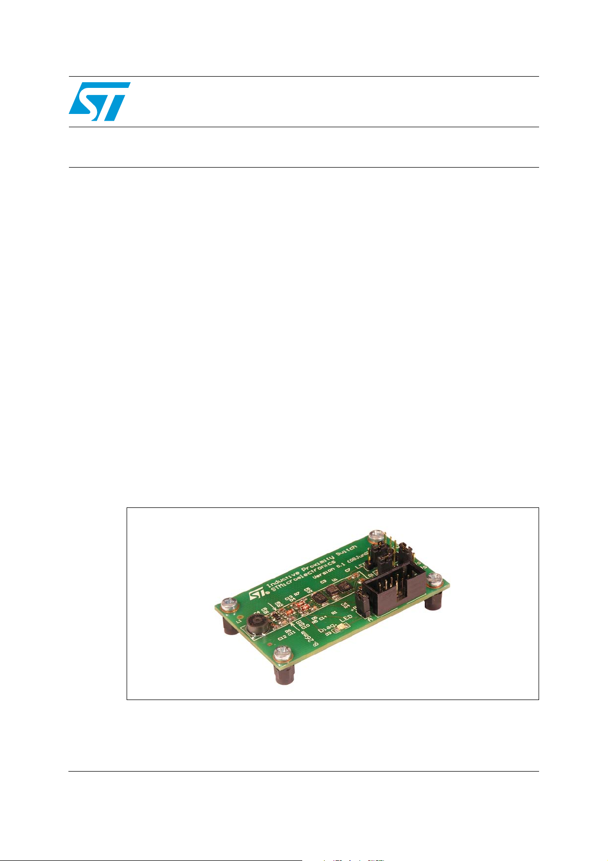
Smart inductive proximity switch
Introduction
The STEVAL-IFS006V1 inductive proximity switch demonstration board is designed based
on the principle of metal body detection using the eddy current effect on the HF losses of a
coil. It consists of a single transistor HF oscillator, an ST7LITEUS5 microcontroller and the
TDE1708DFT intelligent power switch. The board is a compact and cost-effective solution
for an inductive proximity sensor designed for simplicity and for a wide temperature range
and supply voltage variations. Other board features include:
■ Great flexibility: the MCU firmware can be modified depending on application
requirements
■ Sensitivity and hysteresis adjustment
■ In-circuit programming and debugging capabilities
■ Analog and digital temperature compensation
■ PNP and NPN sensor functionality configurations
■ Indicator status LED
■ Overload and short-circuit protection
■ GND and Vs open wire protection
■ Compact design
■ Supply voltage: 6 V to 48 VDC
■ Temperature range: -25 °C to +85 °C
Figure 1. Smart inductive proximity switch demonstration board
July 2008 Rev 1 1/16
www.st.com
Page 2

Contents AN2679
Contents
1 Sensor overview . . . . . . . . . . . . . . . . . . . . . . . . . . . . . . . . . . . . . . . . . . . . 5
2 Sensor circuit description . . . . . . . . . . . . . . . . . . . . . . . . . . . . . . . . . . . . 6
2.1 Initial configuration and jumper settings . . . . . . . . . . . . . . . . . . . . . . . . . . . 6
2.2 Output driver configurations . . . . . . . . . . . . . . . . . . . . . . . . . . . . . . . . . . . . 7
2.3 Application schematic . . . . . . . . . . . . . . . . . . . . . . . . . . . . . . . . . . . . . . . . . 9
2.4 Bill of materials . . . . . . . . . . . . . . . . . . . . . . . . . . . . . . . . . . . . . . . . . . . . . 10
2.5 ICC connector . . . . . . . . . . . . . . . . . . . . . . . . . . . . . . . . . . . . . . . . . . . . . 11
3 Software implementation . . . . . . . . . . . . . . . . . . . . . . . . . . . . . . . . . . . . 12
4 References . . . . . . . . . . . . . . . . . . . . . . . . . . . . . . . . . . . . . . . . . . . . . . . . 14
5 Revision history . . . . . . . . . . . . . . . . . . . . . . . . . . . . . . . . . . . . . . . . . . . 15
2/16
Page 3

AN2679 List of tables
List of tables
Table 1. Initial configuration and jumper settings . . . . . . . . . . . . . . . . . . . . . . . . . . . . . . . . . . . . . . . . 6
Table 2. Low side (NPN) output driver configuration jumper settings. . . . . . . . . . . . . . . . . . . . . . . . . 7
Table 3. High side (PNP) output driver configuration jumper settings . . . . . . . . . . . . . . . . . . . . . . . . 8
Table 4. Bill of materials . . . . . . . . . . . . . . . . . . . . . . . . . . . . . . . . . . . . . . . . . . . . . . . . . . . . . . . . . . 10
Table 5. Diagnostic LED blinking modes (power up self-test) . . . . . . . . . . . . . . . . . . . . . . . . . . . . . 12
Table 6. Diagnostic LED blinking modes (normal operation) . . . . . . . . . . . . . . . . . . . . . . . . . . . . . . 12
Table 7. Document revision history . . . . . . . . . . . . . . . . . . . . . . . . . . . . . . . . . . . . . . . . . . . . . . . . . 15
3/16
Page 4

List of figures AN2679
List of figures
Figure 1. Smart inductive proximity switch demonstration board. . . . . . . . . . . . . . . . . . . . . . . . . . . . . 1
Figure 2. Smart inductive proximity switch block diagram . . . . . . . . . . . . . . . . . . . . . . . . . . . . . . . . . . 5
Figure 3. Initial configuration and jumper settings . . . . . . . . . . . . . . . . . . . . . . . . . . . . . . . . . . . . . . . . 7
Figure 4. Low side (NPN) output driver configuration jumper settings. . . . . . . . . . . . . . . . . . . . . . . . . 7
Figure 5. High side (PNP) output driver configuration jumper settings . . . . . . . . . . . . . . . . . . . . . . . . 8
Figure 6. Smart inductive proximity switch schematic . . . . . . . . . . . . . . . . . . . . . . . . . . . . . . . . . . . . . 9
Figure 7. Inducing the demonstration board self-test. . . . . . . . . . . . . . . . . . . . . . . . . . . . . . . . . . . . . 12
Figure 8. Oscillator amplitude vs. temperature (MCU pin 3) . . . . . . . . . . . . . . . . . . . . . . . . . . . . . . . 13
Figure 9. D2 voltage vs. temperature (MCU pin 5) . . . . . . . . . . . . . . . . . . . . . . . . . . . . . . . . . . . . . . 13
4/16
Page 5
AN2679 Sensor overview
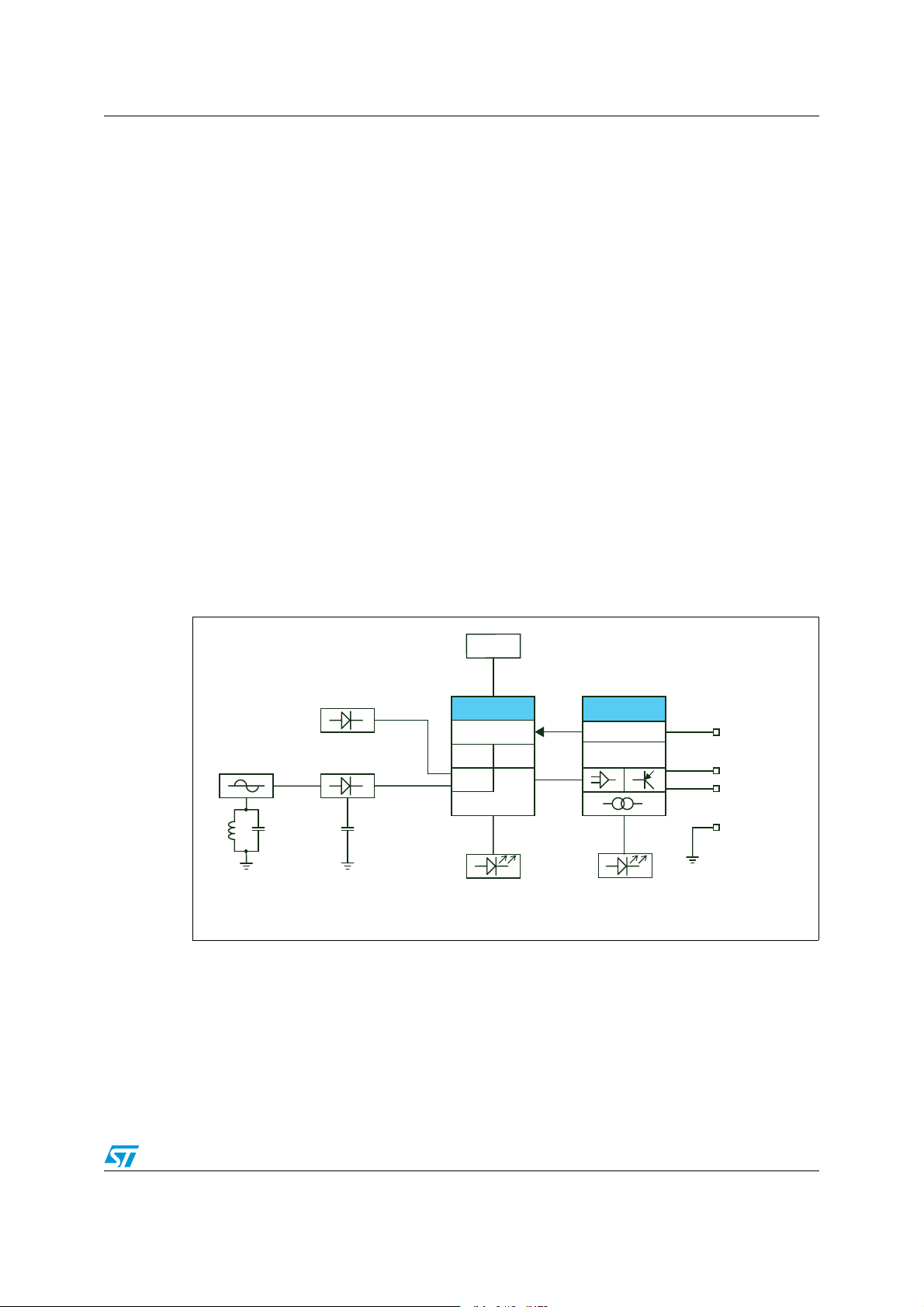
1 Sensor overview
Proximity switches are generally used to sense the position of a moving object in
manufacturing processes. Typically, they utilize an oscillator driver circuit in combination with
an induction tank circuit. The tank circuit includes an induction coil as a means for sensing
the presence of an object such as metal. The magnetic field induces eddy currents in a
conductive object which enters within the generated magnetic field. The oscillation
amplitude is attenuated due to the energy drawn from the induction coil. The amount of the
attenuation is directly related to the distance between the metal object and the induction
coil.
A typical inductive proximity switch employs a ferrite cup core as the sensing element. It
allows the flux field to be focused in front of the cup and to further increase the sensing
distance. The oscillator typically operates between 100 kHz and 800 kHz, where the eddy
current losses are significant.
Some benefits of the MCU approach compared with a traditional solution are:
● more reliable operation thanks to the sensor self-diagnostics
● cheap and easy sensor trimming in the production line
● digital temperature compensation
● linearization of the sensor characteristic
● simple implementation of an analog or PWM output
Figure 2. Smart inductive proximity switch block diagram
)#0
/SCILLATOR
,
^K(Z
#
4EMPSENSOR
$ETECTOR
#
&
M6+
$#TO6
345LTRA,ITE
&,!3(
4)-%23
!$#
BIT
3ELFDIAGNOSTICS,%$
'0)/
+
4$%$&4
6
62%'6
)NDICATORSTATUS,%$
6TO6
3UPPLY6OLTAGE
,O
WSIDEOUTPUT
(IGHSIDEOUTPUT
'.$
!-6
5/16
Page 6

Sensor circuit description AN2679
2 Sensor circuit description
The sensor HF oscillator circuit is based on the Colpitts oscillator type which has a simple
circuit configuration, produces a very clean sinusoidal wave signal and is capable of
oscillating in a wide frequency range. The resonant circuit consisting from the inductor L1
and capacitors C12, C9 and C8 determine the frequency of the oscillations according to the
formula in Equation 1. Actually the circuit will oscillate at a slightly lower frequency due to
coupling capacitor C10, junction capacitances of transistor Q1 and other stray capacitances.
Equation 1
f
------------------------------------------------------------- -=
2π
The oscillator employs a transistor, Q1, operating in a common base configuration that
derives its feedback from the capacitor divider C9 andC8. Resistors R3 and R6 set its bias
point and the temperature of diode D2 stabilizes it.
The oscillator signal amplitude is further detected by diodes D4 and D5, and filtered by
capacitor C13. Together with C10 this circuit acts as a charge pump, thus the full range of
the ST7 ADC converter (0 V - 5 V) is used.
1
12
C8C
--------------------- -+
C8C9+
9
⎛⎞
L1C
⎜⎟
⎝⎠
The other function of diode D2 is temperature sensing. The voltage across a diode operated
at constant current is linear in a very large range of temperature and reduces with
increasing temperature by approximately -2 mV/ k (see Figure 9). With the ST7 10-bit ADC
converter, the temperature can be measured with an accuracy of approximately 2.5 °C
which is enough for overall correction of the sensor temperature variations (see Figure 8).
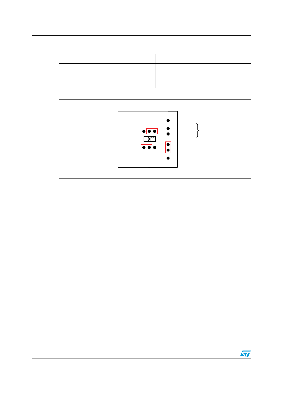
2.1 Initial configuration and jumper settings
Ta bl e 1 and Figure 3 represent the initial (high side) output driver configuration and jumper
settings. The diagnostic LED D3 shares the MCU pin 2 with the ICC connector. In case of
programming/debugging problems, it can be disconnected by removing the jumper from
pins P14 and P15.
Table 1. Initial configuration and jumper settings
Pins Setting
P10 - P11 A - HS
P4 - P5 LED - C
P3 - P7 +Vs - LS
P14 - P15 +5V - A
6/16
Page 7

AN2679 Sensor circuit description
Figure 3. Initial configuration and jumper settings
$
!(3
$
'.
'.
(3
$
,OAD
0OWER
3UPPLY
,%$#
6
6S
!
!-6
2.2 Output driver configurations
The demonstration board output can be configured using the jumpers for low side (see
Ta bl e 2 and Figure 4) and/or high side (Ta bl e 3 and Figure 5) functionality.
Table 2. Low side (NPN) output driver configuration jumper settings
Pins Setting
P9 - P10 LED - A
P5 - P6 C - LS
P8 - P12 HS - GND
Figure 4. Low side (NPN) output driver configuration jumper settings
,%$!
$
#,3
'.$
,3
6S
6S
,OAD
!-6
7/16
Page 8
Sensor circuit description AN2679
Table 3. High side (PNP) output driver configuration jumper settings
Pins Setting
P10 - P11 A - HS
P4 - P5 LED - C
P3 - P7 +Vs - LS
Figure 5. High side (PNP) output driver configuration jumper settings
!(3
$
,%$#
'.$
'.
(3
6S
$
,OAD
!-6
8/16
Page 9

AN2679 Sensor circuit description
2.3 Application schematic
Figure 6. Smart inductive proximity switch schematic
P1
+Vs1P3
+Vs1P7
LS
1
C2
10nF
C1
D1
1
P6
LS
1
P5
C
1
P4
LED
100nF
Status LED
P8
HS1P12
GND1P13
GND
1
PA0
PA1
R4
10nF
C7
1
P11
HS
1
P10
A
1
P9
LED
10K
8
Vss
7
PA0/AIN0/ATPWM/ICCDATA
6
5
PA2/LTIC/AIN2
PA1/AIN1/ICCCLK
9
7
+Vs
VREG +5V
U1
TDE1708DFT
6
+5V
PA3
0
R1
PA1
PA0
10
8
2
4
6
GND
RESET
ICCCLK
ICCDATA
GND
GND
GND
Vdd
P2
+5V
CLKIN
Con ICC
1
3
5
7
9
PA5
4
2
1
8
L. S. OUT
LED DRIVER
IN
5
PA0
H. S. OUT
GND
9
C8
R2
D2
1.5nF
4.7K
1N4148
+5V +5V
P15
A
P14
+5V
+5V
DELAY
3
10nF
C3
10uF/6.3V
C6
100nF
C5
+5V
C4
100nF
+5V
1
1
1.5K
R3
Vdd1PA5/AIN4/CLKIN2PA4/AIN33PA3/RESET
U2
ST7LITEUS5
1.5K
R5
D3
Diag. LED
D4
C10
100pF
C9
Q1
BC857B
PA5
1N4148
47pF
4
C14
10nF
PA3
R7
220K
1.5nF
C13
D5
1N4148
470pF
C12
L1
10K
R6
10nF
C11
9/16
Page 10

Sensor circuit description AN2679
2.4 Bill of materials
Table 4. Bill of materials
Reference Value Description Quantity Supplier Order code
U1 Intelligent power switch 1 STMicroelectronics TDE1708DFT
U2 8-bit MCU 1 STMicroelectronics ST7FLITEUS5U3
C1, C7 10 nF Capacitor 2 EPCOS B37941A1103K0xx
C2 100 nF Capacitor 1 EPCOS B37941A5104K0xx
C3, C11, C14 10 nF Capacitor 3 EPCOS B37931A5103K0xx
C4, C5 100 nF Capacitor 2 EPCOS B37931K0104K0xx
C6 10 µF/6.3 V Polarized capacitor 1
C8, C13 1.5 nF Capacitor 2 EPCOS B37931A5152K0xx
C9 100 pF Capacitor 1 EPCOS B37930A5101J0xx
C10 47 pF Capacitor 1 EPCOS B37930A5470J0xx
C12 470 pF Capacitor 1 EPCOS B37930A5471J0xx
D1 Status LED LED 1
D2, D4, D5 1N4148 Diode 3
D3 Diag. LED LED 1
L1 68 µH PS-core inductor 1 Bohemia Electric BES070815
Core EPCOS B65933A0000X022
Coil former EPCOS B65512C0000T001
P1, P3 +Vs Header, 1-pin 2
P2 Con ICC ICC connector 1
P4, P9 LED Header, 1-pin 2
P5 C Header, 1-pin 1
P6, P7 LS Header, 1-pin 2
P8, P11 HS Header, 1-pin 2
P10, P15 A Header, 1-pin 2
P12, P13 GND Header, 1-pin 2
P14 +5 V Header, 1-pin 1
Q1 BC857B PNP transistor 1
R1 0 Resistor 1
R2 4.7 kΩ Resistor 1
R3, R5 1.5 kΩ Resistor 2
R4, R6 10 kΩ Resistor 2
R7 220 kΩ Resistor 1
10/16
Page 11

AN2679 Sensor circuit description
2.5 ICC connector
The board ICC connector offers in-circuit programming and debugging capabilities and thus
simplifies the firmware development. More information about ST7 development tools is
available from www.st.com/mcu.
11/16
Page 12

Software implementation AN2679
#
O
3 Software implementation
After the first start-up following the firmware upload, the ST7 MCU performs a simple board
self-test. It reads the oscillator amplitude level and voltage across the temperature-sensing
diode D2 and checks whether these values are within a specific range (this state is indicated
by blinking diagnostic LED D3; see Ta bl e 5 ). The oscillator amplitude level detected during
this test is also considered as an initial oscillator level when no metal object approaches the
sensing inductor L1, and its value is recorded to the Flash memory (address 0xfc00) using
an in-application programming (IAP) method. This value is later used for amplitude
reduction comparisons caused by metal objects.
Note: The initial board self-test procedure can be performed at any time by placing a jumper
on pins 3 and 4 of the ICC connector (see Figure 7) and powering up the application.
Figure 7. Inducing the demonstration board self-test
#ON)##
During normal operation, the MCU then controls the sensor output based of the information
about the oscillator amplitude and the actual temperature. The main sensor part of the
firmware is implemented in an auto-reload timer interrupt service routine. In equidistant time
intervals the oscillator amplitude is sampled and its value is compared with two system
variables (ucUpperCompThreshold and ucLowerCompThreshold). One of these defines the
ON to OFF transition, and the other defines the OFF to ON transition of the sensor state.
The distance between them determines the hysteresis. These threshold variable values are
defined as a percentage of the initial oscillator level recorded in the Flash memory and are
further modified depending on the temperature by a coefficient from a lookup table.
Table 5. Diagnostic LED blinking modes (power up self-test)
LED status Meaning
Blinking Input values within limits
Constant Error
Table 6. Diagnostic LED blinking modes (normal operation)
Flashing style Meaning
❋ ❋ ❋ ❋ ❋ ❋ Under-temperature
❋❋ ❋❋ ❋❋ ❋❋ Over-temperature
❋❋❋ ❋❋❋ ❋❋❋ Ferrite approaching the coil
12/16
Page 13

AN2679 Software implementation
Figure 8. Oscillator amplitude vs.
temperature (MCU pin 3)
Figure 9. D2 voltage vs. temperature (MCU
pin 5)
13/16
Page 14

References AN2679
4 References
1. ST7LITEUS5 datasheet
2. TDE1708DFT datasheet
3. Application note AN495
4. EN60947-5-2: "Low-voltage switchgear and controlgear - Part 5-2: Control circuit
devices and switching elements - Proximity switches"
14/16
Page 15

AN2679 Revision history
5 Revision history
Table 7. Document revision history
Date Revision Changes
07-Jul-2008 1 Initial release.
15/16
Page 16

AN2679
Please Read Carefully:
Information in this document is provided solely in connection with ST products. STMicroelectronics NV and its subsidiaries (“ST”) reserve the
right to make changes, corrections, modifications or improvements, to this document, and the products and services described herein at any
time, without notice.
All ST products are sold pursuant to ST’s terms and conditions of sale.
Purchasers are solely responsible for the choice, selection and use of the ST products and services described herein, and ST assumes no
liability whatsoever relating to the choice, selection or use of the ST products and services described herein.
No license, express or implied, by estoppel or otherwise, to any intellectual property rights is granted under this document. If any part of this
document refers to any third party products or services it shall not be deemed a license grant by ST for the use of such third party products
or services, or any intellectual property contained therein or considered as a warranty covering the use in any manner whatsoever of such
third party products or services or any intellectual property contained therein.
UNLESS OTHERWISE SET FORTH IN ST’S TERMS AND CONDITIONS OF SALE ST DISCLAIMS ANY EXPRESS OR IMPLIED
WARRANTY WITH RESPECT TO THE USE AND/OR SALE OF ST PRODUCTS INCLUDING WITHOUT LIMITATION IMPLIED
WARRANTIES OF MERCHANTABILITY, FITNESS FOR A PARTICULAR PURPOSE (AND THEIR EQUIVALENTS UNDER THE LAWS
OF ANY JURISDICTION), OR INFRINGEMENT OF ANY PATENT, COPYRIGHT OR OTHER INTELLECTUAL PROPERTY RIGHT.
UNLESS EXPRESSLY APPROVED IN WRITING BY AN AUTHORIZED ST REPRESENTATIVE, ST PRODUCTS ARE NOT
RECOMMENDED, AUTHORIZED OR WARRANTED FOR USE IN MILITARY, AIR CRAFT, SPACE, LIFE SAVING, OR LIFE SUSTAINING
APPLICATIONS, NOR IN PRODUCTS OR SYSTEMS WHERE FAILURE OR MALFUNCTION MAY RESULT IN PERSONAL INJURY,
DEATH, OR SEVERE PROPERTY OR ENVIRONMENTAL DAMAGE. ST PRODUCTS WHICH ARE NOT SPECIFIED AS "AUTOMOTIVE
GRADE" MAY ONLY BE USED IN AUTOMOTIVE APPLICATIONS AT USER’S OWN RISK.
Resale of ST products with provisions different from the statements and/or technical features set forth in this document shall immediately void
any warranty granted by ST for the ST product or service described herein and shall not create or extend in any manner whatsoever, any
liability of ST.
ST and the ST logo are trademarks or registered trademarks of ST in various countries.
Information in this document supersedes and replaces all information previously supplied.
The ST logo is a registered trademark of STMicroelectronics. All other names are the property of their respective owners.
© 2008 STMicroelectronics - All rights reserved
STMicroelectronics group of companies
Australia - Belgium - Brazil - Canada - China - Czech Republic - Finland - France - Germany - Hong Kong - India - Israel - Italy - Japan -
Malaysia - Malta - Morocco - Singapore - Spain - Sweden - Switzerland - United Kingdom - United States of America
www.st.com
16/16
 Loading...