


AN2668
Application note
Improving STM32F101xx and STM32F103xx
ADC resolution by oversampling
Introduction
The STMicroelectronics Medium- and High-density STM32F101xx and STM32F103xx
Cortex™-M3 based microcontrollers come with 12-bit enhanced ADC sampling with a rate
up to Msamples/s. In most applications, this resolution is sufficient, but in some cases where
higher accuracy is required, the concept of oversampling and decimating the input signal
can be implemented to save the use of an external ADC solution and to reduce the
application consumption.
This application note gives two methods to improve ADC resolution. These techniques are
based on the same principle: oversampling the input signal with the maximum 1 MHz ADC
capability and decimating the input signal to enhance its resolution.
The method and the firmware given within this application note apply to both Medium- and
High-density STM32F10xxx products. Some specific hints are given at the end of the
application note to take advantage of the Medium- and High-density STM32F103xx
performance line devices and of the High-density STM32F101xx access line devices.
This application note is split into two main parts: the first one describes how oversampling
increases the ADC-specified resolution while the second describes the guidelines to
implement the different methods available and gives the firmware flowchart of their
implementation on the STM32F101xx and STM32F103xx devices.
July 2008 Rev 1 1/21
www.st.com

Contents AN2668
Contents
1 Definition of ADC signal-to-noise ratio . . . . . . . . . . . . . . . . . . . . . . . . . . 4
2 Nyquist theorem and oversampling . . . . . . . . . . . . . . . . . . . . . . . . . . . . 5
3 Oversampling using white noise . . . . . . . . . . . . . . . . . . . . . . . . . . . . . . . 6
3.1 SNR of oversampled signal with white input noise . . . . . . . . . . . . . . . . . . . 6
3.2 Decimation . . . . . . . . . . . . . . . . . . . . . . . . . . . . . . . . . . . . . . . . . . . . . . . . . 6
3.3 When is this method efficient? . . . . . . . . . . . . . . . . . . . . . . . . . . . . . . . . . . 7
3.4 Method implementation on the STM32F10xxx devices . . . . . . . . . . . . . . . 8
3.4.1 Oversampling using a white noise firmware flowchart . . . . . . . . . . . . . . . 9
3.4.2 Oversampling using white noise result evaluation . . . . . . . . . . . . . . . . . 10
4 Oversampling using triangular dither . . . . . . . . . . . . . . . . . . . . . . . . . . 12
4.1 When does this method work? . . . . . . . . . . . . . . . . . . . . . . . . . . . . . . . . . 12
4.2 Method implementation on STM32F10xxx devices . . . . . . . . . . . . . . . . . 13
5 Comparing the first and second methods . . . . . . . . . . . . . . . . . . . . . . 15
6 Hints . . . . . . . . . . . . . . . . . . . . . . . . . . . . . . . . . . . . . . . . . . . . . . . . . . . . . 16
6.1 What is the maximum number of bits that can be added to
the on-chip ADC resolution? . . . . . . . . . . . . . . . . . . . . . . . . . . . . . . . . . . 16
6.2 Taking advantage of High-density STM32F10xxx devices . . . . . . . . . . . . 16
6.3 Taking advantage of the Medium- and High-density performance line
(STM32F103xx) devices 17
Appendix A Quantization error . . . . . . . . . . . . . . . . . . . . . . . . . . . . . . . . . . . . . . . 18
Revision history . . . . . . . . . . . . . . . . . . . . . . . . . . . . . . . . . . . . . . . . . . . . . . . . . . . . 20
2/21

AN2668 List of figures
List of figures
Figure 1. Oversampling effect on the quantization noise . . . . . . . . . . . . . . . . . . . . . . . . . . . . . . . . . . . 6
Figure 2. Histogram analysis . . . . . . . . . . . . . . . . . . . . . . . . . . . . . . . . . . . . . . . . . . . . . . . . . . . . . . . . 8
Figure 3. Histogram analysis for DC = 1.65 V . . . . . . . . . . . . . . . . . . . . . . . . . . . . . . . . . . . . . . . . . . . 9
Figure 4. Oversampling using a white noise flowchart. . . . . . . . . . . . . . . . . . . . . . . . . . . . . . . . . . . . 10
Figure 5. Ramp samples with 1 additional bit . . . . . . . . . . . . . . . . . . . . . . . . . . . . . . . . . . . . . . . . . . 11
Figure 6. Ramp samples with 2 additional bits . . . . . . . . . . . . . . . . . . . . . . . . . . . . . . . . . . . . . . . . . 11
Figure 7. How to perform oversampling by adding a triangular signal . . . . . . . . . . . . . . . . . . . . . . . 12
Figure 8. Hardware requirements of oversampling by adding a triangular signal . . . . . . . . . . . . . . . 13
Figure 9. Oversampling using triangular dither flowchart. . . . . . . . . . . . . . . . . . . . . . . . . . . . . . . . . . 14
Figure 10. Oversampling effect on the quantization error . . . . . . . . . . . . . . . . . . . . . . . . . . . . . . . . . . 18
3/21

Definition of ADC signal-to-noise ratio AN2668
SNR
dB
6.02N 1.76+=
1 Definition of ADC signal-to-noise ratio
The ADC gives a representation of an analog signal among a finite number of digital words.
Since the digital domain is represented by a finite number of words which have to present a
continuous signal, the conversion step introduces the quantization error function of the ADC
input range and resolution.
For an ideal ADC, the quantization error is between ±0.5 LSB. In the case where the input
signal is varying through many levels between samples, and the sampling rate is not
synchronized with the input frequency, the quantization error can be considered as a white
noise whose energy is uniformly spread from the DC domain to half of the sampling
frequency. Please refer to Appendix A for more details regarding the calculation of its
density.
The SNR (signal-to-noise ratio) is the ratio of the ADC noise to the input signal power. For
an ideal ADC, it is assumed that the SNR is equal to the quantization noise (no other noise
source is considered) to the input signal. It is demonstrated that for a full-scale sinusoidal
signal, the ADC SNR is maximum and given by the following formula:
, where N is the ADC resolution.
It is can be easily noticed that when the SNR increases, the ADC effective number of bits
increases.
For a real ADC, different error sources should be considered: offset, gain, INL (integral
nonlinear) and DNL (differential nonlinear). A brief description of these errors can be found
in the STM32F101xx and STM32F103xx datasheets. They degrade the ideal ADC
resolution. In this case, we speak of real effective number of bits.
Improving the SNR involves an enhancement of the ADC effective number of bits.
The following section demonstrates that sampling the input signal with higher rates than the
Nyquist frequency improves the SNR. The Nyquist frequency is introduced in the next
paragraph.
4/21

AN2668 Nyquist theorem and oversampling
2 Nyquist theorem and oversampling
The Nyquist theorem states that in order to be able to reconstruct the analog input signal,
the signal should be sampled at a rate f
maximum frequency component of the input signal.
Not respecting the Nyquist theorem causes aliasing effects and the analog signal cannot be
fully reconstructed from the input samples. Therefore, in most applications, a low-pass filter
is required at the ADC input to filter frequencies lower than half the sampling frequency. It is
difficult to handle the filter constraints with low sampling frequencies.
Oversampling consists in sampling the input analog signal at rates higher than the Nyquist
frequency limit, filtering the samples and reducing the sample rate by decimation. Using this
method relaxes the anti-aliasing low-pass filter constraints.
(sampling frequency) that is greater than twice the
S
5/21
Oversampling using white noise AN2668
SNR
OVS
6.02 N 1.76+⋅ 10 OS R()log+=
F
OVS
4pF
S
=
3 Oversampling using white noise
3.1 SNR of oversampled signal with white input noise
Let us assume that the quantization noise is assimilated to white noise. Then its power
density is uniformly distributed between DC and half the Nyquist frequency. This power
density is independent of the sampling frequency.
When sampling at higher rates, the quantization noise is spread over the bandwidth of the
sampling frequency.
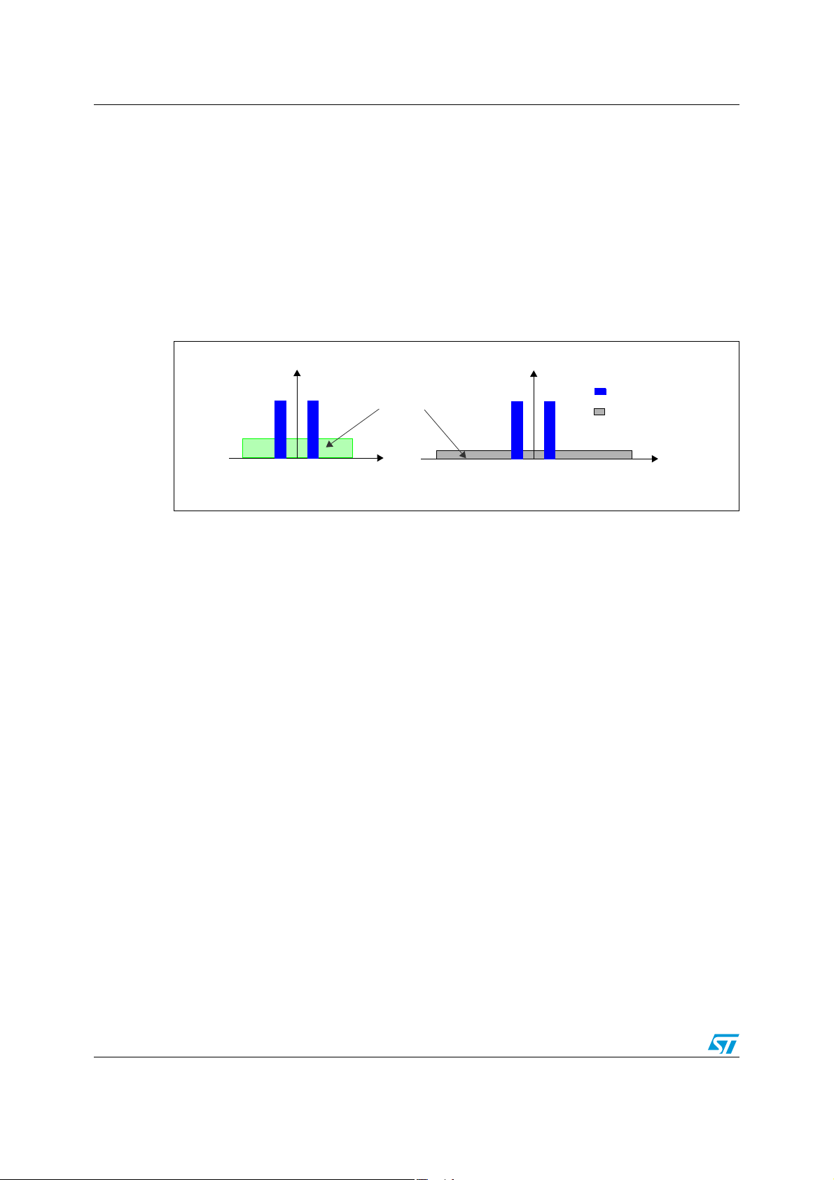
Figure 1. Oversampling effect on the quantization noise
-2.f
PSD
Same area
- f
m
m
fS = 2.f
f
m
F
m
-2.N.f
m
PSD
Input signal
Quantization error
PSD = Power signal density
F
- f
f
m
m
fS= 2.N.f
m
ai14937
According to Figure 1, when sampling the input signal at higher rates, the same noise
power, represented by the area of the green rectangle, is spread over a bandwidth equal to
the sampling frequency which is much greater than the signal bandwidth fm. Only a
relatively small fraction of the total noise power falls in the [–fm, fm] band, and the noise
power outside the signal band can be greatly attenuated with a digital low-pass filter.
Reducing the quantization noise enhances the signal-to-noise ratio and, consequently, the
ADC effective number of bits. Oversampling the input signal OSR times faster than the
Nyquist frequency gives the following SNR
It can be concluded that each doubling of the sampling frequency will lower the in-band
noise by 3 dB, and increase the measurement resolution by 1/2 bit. Therefore, 6dB SNR
gain is required to add 1 resolution bit to the ADC.
In general, if p additional bits are required by the application then, the ADC sampling
frequency should be at least:
, where F
is the current ADC sampling frequency used.
S
3.2 Decimation
The conventional meaning of averaging is adding m samples and dividing the result by m.
Averaging several data from an ADC measurement is equivalent to a low-pass filter which
attenuates the signal fluctuation and noise. The average method is often used to smooth
and remove speaks from the input signal.
Note that normal averaging does not increase the resolution of the conversion because the
sum of m N-bit samples divided per m is an N-bit representation of the sample.
6/21

AN2668 Oversampling using white noise
Decimation is an averaging method. When combined with oversampling, decimation
improves the ADC resolution.
In fact, adding 4
p
ADC N-bit samples, gives a representation of the signal on N+2p bits. In
order to have p additional effective bits, the sum is shifted to the right by p bits.
This FIR filter with equal filter coefficients enables the user to filter the oversampling
frequency by giving an output sample computed from the OSR input samples.
The oversampling method limits the maximum input frequency bandwidth. In fact, in the
case of the STM32F10xxx, signals having components up to 500 kHz can be processed by
the ADC. If for example, two additional resolution bits are required, then the maximum input
frequency that can be entered is 500 kHz/16 = 31.25 kHz when oversampling using white
noise.
3.3 When is this method efficient?
For the oversampling and decimating method to work properly, the following requirements
must be satisfied:
● There should be some noise in the input signal. This noise must approximate white
noise with a uniform power spectral density over the frequency band of interest.
● The noise amplitude must be sufficient to toggle the input signal randomly from sample
to sample by an amount of at least 1 LSB. Otherwise, the input samples would have the
same representation and the sum and average operations would not give any extra
resolution. In most applications, the internal ADC thermal noise and the input signal
noise are sufficient to use this method. In the case where the thermal noise does not
have a high-enough amplitude to toggle the input signal randomly, then artificial white
noise should be injected into the input signal. This operation is referred to as
“dithering”. Regarding this point, two questions can be raised. The first is “How to
evaluate the ADC noise and test its Gaussian criteria?” and “How to generate white
noise if needed?”
– A practical way of detecting the Gaussian criteria of the input signal noise is to see
the distribution of a clean DC signal over the ADC codes. The histogram method
can be used to verify if the input noise follows a Gaussian distribution. The
example in Figure 2 shows two possible situations.
7/21

Oversampling using white noise AN2668
ADC codes
N N+1 N+2N–1N–2
Histogram for a signal with white noise
ADC codes
N N+1 N+2N–1N–2
Histogram for a signal without white noise
ai14938
Figure 2. Histogram analysis
– In the case where external noise dither should be added to the input signal, then
the thermal noise generated by a diode or a resistor can be injected into the input
signal.
– The input noise should not correlate with the useful input signal and the input
signal should have equal probability to be between two adjacent ADC codes. This
means that for systems using feedback process, this method does not work.
3.4 Method implementation on the STM32F10xxx devices
This method describes the different steps undertaken to implement and test the
oversampling method on the STM32F10xxx devices.
According to the previous section, in order to make this solution work properly, there should
be some white noise to make the input signal toggle randomly by 1/2 LSB. For this, the
application environment noise should be considered.
The first step consists in computing the STM32F10xxx ADC thermal noise to conclude if
external white noise should be injected into the input signal. In a typical application board,
the computed noise does not include only the ADC internal noise but also the possible noise
generated by the different board components and the layout. Therefore, this evaluation
depends on the application board but the methodology remains the same.
The histogram method is used for different DC input voltages. This input voltage is sampled
a large number of times (example 5000). The related distribution can be easily interpreted
using a spreadsheet.
For example, for a 1.65 V DC input voltage applied on the STM3210B-EVAL evaluation
board, the histogram shown in Figure 3 is detected.
8/21

AN2668 Oversampling using white noise
ai14939
Figure 3. Histogram analysis for DC = 1.65 V
The ADC thermal noise can be computed from this histogram (though this can be shown, it
is not the objective of this application note and details are not offered here).
In order to carry on this ADC noise test, the user should do the following:
● uncomment the line #define Themal_Noise_Measure in the oversampling.h file
● configure the Total_Samples_Number which is the number of ADC conversion
operations. It should be smaller than 65535. The DMA channel is configured to store
the number of ADC samples in a RAM buffer. At the end of the transfer, an interrupt is
generated and the number of occurrences of each ADC code is computed
● In order to compute the occurrence of the ADC codes, a variable giving the relevant
ADC codes is defined
When the code is run, Relevant_ADC_Samples ADC samples and their corresponding
number of occurrences are displayed on the HyperTerminal. The HyperTerminal
configuration is 8-bit data, no parity, 115 200 baud rate. If the effective number of ADC
samples found is smaller than the defined Relevant_ADC_Samples variable, then 0 is
displayed for both ADC code and ADC code occurrence. The user can capture them and
build a histogram.
3.4.1 Oversampling using a white noise firmware flowchart
The STM32F10xxx on-chip ADC conversion frequency is fixed to 1 MHz. The ADC DMA
channel is configured to transfer the number of oversampled inputs from the ADC data
register to a buffer in RAM. This transfer is configured to occur one time. At the end of the
DMA transfer, an interrupt is triggered and the oversampled result is computed.
The STM32F10xxx general-purpose timer TIM2 is used to generate the input signal
sampling frequency. For this, the TIM2 reference clock is configured at 1 µs. Its period
determines the input signal sampling period. It is defined in the oversampling.h file as
#define Input_Signal_Sampling_Period. When the TIM2 update interrupt is
triggered, the DMA is re-enabled and the converted ADC values can be treated. Figure 4
summarizes the implemented functionality.
9/21

Oversampling using white noise AN2668
Sampling period = TIM2 period
ADC period = 1 µs
TIM2 update interrupt
Clear flag
Enable DMA
Time t
<=1µs
DMA transfer complete interrrupt
Clear DMA Interrupt pending bit
Compute the oversampled result
Update DMA counter and pointer
Disable DMA
ai14940
Figure 4. Oversampling using a white noise flowchart
The oversampled data are computed in the DMA transfer complete interrupt. For
synchronization reasons, it is recommended to read it in the second TIM2 interrupt.
Note that with this implementation, the TIM2 period should be greater than the time required
by the ADC to convert OSR samples, and greater than the ADC interrupt execution time.
If the sampling frequency required by the application is exactly OSR µs, then the user is not
required to use Timer TIM2 to generate the input sampling frequency. However, the DMA
should be configured to be functional in continuous mode and the DMA transfer complete
interrupt should be updated accordingly. The oversampled data are usually computed in the
DMA transfer complete interrupt.
3.4.2 Oversampling using white noise result evaluation
In order to evaluate the oversampling method, the user should uncomment the #define
Oversampling_Test line and configure the number of samples with the enhanced
resolution.
When this line is uncommented, a buffer is created in RAM to store the oversampled data.
The buffer contents are then displayed on the HyperTerminal. The HyperTerminal
configuration should be 8-bit data, no parity and 115 200 baud rate. The user can capture
them into a txt file and then compare the expected results to the real ones.
In order to evaluate the new enhanced ADC, a ramp with a 50 Hz frequency and a 1 V
amplitude is input into the ADC and sampled using the oversampling algorithm every 50 µs.
The firmware example related to this method is located in the WhiteNoiseMethod folder.
10/21

AN2668 Oversampling using white noise
50 H/1 V - 1 additional bit
3000
2500
2000
1500
1000
500
0
0
30
60
90
120
150
180
210
240
270
300
330
360
390
ai14942
50 H/1 V - 2 additional bits
6000
5000
4000
3000
2000
1000
0
0
41
82
123
164
205
246
287
328
369
410
451
492
533
574
615
656
697
738
779
ai14942
Figure 5. Ramp samples with 1 additional bit
Figure 6. Ramp samples with 2 additional bits
The oversampling algorithm using white noise is run with the same ramp (50 Hz frequency
and 1 V amplitude). Both Figure 5 and Figure 6 give the ADC oversampled data as a
function of time in µs. Figure 5 is the result of adding one bit while Figure 6 is the result of
adding two additional bits to the ADC on-chip resolution.
When the ramp is sampled without using any extra software resolution, with a 3.3 V
reference supply, 1 V corresponds to the digital value 1250.
When one additional bit is added, 1 V is sampled as 2500 and when two additional bits are
added, 1 V is sampled as 5000.
This means that the environment contains enough noise for this method to work.
11/21

Oversampling using triangular dither AN2668
q0
q1
Input signal @ q0+0.6LSB
Input signal + triangular
waveform samples q1
(q1+q0)/2
(q1+q0)/4
(q1+q0)/8
Average of q1 occurrences= 9/16 = 0.563
Result =(7x110 000+ 9x111 000 + 1) >>1=110 101
110 000
110 001
110 010
110 011
110 100
110 101
110 110
110 111
111 000
waveform samples q0
Input signal + triangular
-> The nearest value is 110 101
ai14943
SNR
Gain
20.
OSR
2
-------------
⎝⎠
⎛⎞
log=
F
OVS
2.2pF
S
=
4 Oversampling using triangular dither
Assuming that the input signal is between two successive quantization steps q0 and q1
during the oversampling period, then the converter may convert it either to q0 or q1. Adding
extra p bits of resolution means determining the relative position of the input signal between
q0 and q1.
With the addition of an appropriate triangular signal, the quantizer generates a series of q1s
and q0s. Averaging the q1 occurrences over a given interval determines the relative position
of the input signal between the lower and the higher quantization steps.
The theory states that the best results are achieved when dithering the input signal using a
triangular waveform with a period of OSR times the ADC sampling period and an amplitude
of n+0.5LSB where n = 0,1,2,3.
The theory behind this methods is quite complicated, so that Figure 7 serves as an example
to illustrate how this method works. In this example, the ADC on-chip resolution is 3 and
three extra bits are added by firmware. The input signal is assumed to have an amplitude of
q0+ 0.6LSB (q0 = 6 in this example). In order to add three additional bits, the input signal is
sampled 2.2
Figure 7. How to perform oversampling by adding a triangular signal
3
times (16 times).
If the input signal is not correlated with the triangular waveform, then it is demonstrated that
the gain in the SNR is equal to
Therefore, each doubling of the sampling frequency improves the SNR by 6dB and adds 1
ADC bit resolution.
In general, in order to add p-bit extra resolution, the oversampling frequency should be
equal to
4.1 When does this method work?
In order to make this method work, the input signal should not vary by more than ±0.5LSB
during the oversampling period and should not correlate with the triangular dither signal.
12/21

AN2668 Oversampling using triangular dither
Input signal
10 kΩ
VDD
-
+
PWM output
RC to filter the PWM
frequency
-
V
DD
/2
V
DD
/2
0
V
DD
4 MΩ
ADC Input
Vs
1 kΩ
1 kΩ
R2
10 kΩ
R1
R3
100 nF
0.46 kΩ
5.5 nF
ai14944
4.2 Method implementation on STM32F10xxx devices
In order to implement the second solution, the following is needed:
● An operational amplifier to perform the sum of the input signal and the triangular
waveform. For this, an op-amp inverter/summing stage is required. The ST component
LMV321 can be used.
● Triangular waveform with a period of OSR times the ADC conversion rate. The user can
either use a signal generator or one of the STM32F10xxx on-chip timers and an RC
network to generate this triangular signal. Indeed, the on-chip timer generates a PWM
signal with a duty cycle varying from 0 to 100%. This PWM output can be filtered with
an RC filter to generate a triangular signal varying from 0 to V
an amplitude of 0.5LSB, then the output is first passed through a capacitor (to cut the
DC component) and then divided by the prescaler R2/R3 (see Figure 8). This prescaler
is equal to the ADC number of words.
● The input signal should not be changed after the op-amp. For this reason, R1 should be
equal to R3.
● The sum of the input signal and the triangular dither is inverted. For this purpose, a
3.3 V offset is required on the positive entry of the op-amp. After the oversampled data
are computed, this offset is subtracted to give the input signal estimation with extra
resolution.
. In order to generate
DD
Figure 8. Hardware requirements of oversampling by adding a triangular signal
The STM32F10xxx on-chip ADC conversion frequency is fixed at 1 MHz. The ADC DMA
channel is configured to transfer the number of oversampled inputs from the ADC data
register to a buffer in RAM. This transfer is configured to occur one time. At the end of the
DMA transfer, an interrupt is triggered and the oversampled result is computed.
The STM32F10xxx general-purpose timer TIM2 is used to generate the input signal
sampling frequency. For this, the TIM2 reference clock base is configured at 1 µs. Its period
determines the input signal sampling period. It is defined in the oversampling.h file by
#define Input_Signal_Sampling_Period.
The triangular dither is generated using Timer TIM3 configured in PWM mode by updating
the Capture Compare Register CCR1. Timer TIM3 period should be equal to the ADC
conversion rate and CCR1 should be updated OSR times where OSR is the oversampling
factor. In order to do this, the possible CCR1 values are first computed and stored into a
RAM buffer, then DMA transfer is used to update the CCR1 register, removing the need for
interrupts.
Note that the ADC conversion rate limits the oversampling factor. For example, in the case
where the ADC is running at 1 MHz, the STM32F10xxx is operating at 56 MHz. In order to
13/21

Oversampling using triangular dither AN2668
Sampling period = TIM2 period
ADC period = 1 µs
TIM2 Update interrupt
Clear flag
Enable ADC DMA
Time t
<=1µ
ADC DMA transfer complete interrupt
Clear DMA Interrupt pending bit
Compute the oversampled result
Update ADC DMA counter and pointers
Disable DMA
Enable TIM3 DMA
Update TIM3 DMA counter and pointers
TIM 3 period = ADC period = 1 µs
TIM3 CCR1 register varies during OSR period (OSR = 4 in this example)
Input signal dithered with the
triangular signal
Input signal
ai14945
have a period of 1 µs, the auto-reload register of timer TIM3 should be equal to 55. The
maximum number of additional bits is then 4.
When a TIM2 update interrupt is triggered, the ADC and TIM3 DMA are re-enabled and the
converted ADC values can be treated to compute the new sample with the extra resolution
bits. Figure 9 summarizes the implemented functionality.
Figure 9. Oversampling using triangular dither flowchart
For this method to work, the input signal should not vary by more than ±0.5LSB during the
oversampling period. This means that for an STM32F10xxx operating from a 3.3 V VDD
power supply, the maximum allowed variations of the input signal during the oversampling
period is ~0.4 mV.
On the other side, a triangular waveform with an amplitude of 0.5LSB means a 0.4 mV
amplitude when operating the STM32F10xxx from a 3.3 V power supply. The application
environment must therefore not be very noisy. Any disturbance of the triangular waveform
will have an impact on the computed oversampled data.
According to the implementation, the triangular waveform is generated by means of the
STM32F10xxx timer and an RC filter that cuts the 1 MHz timer frequency. The timer PWM
output signal is integrated to provide a triangular signal with a 3.3 V amplitude. The division
is done with the ratio R4/R2.
The firmware related to this method is located in the TriangularDitherMethod
directory.
14/21

AN2668 Comparing the first and second methods
5 Comparing the first and second methods
The first method based on oversampling and averaging using white noise provides a half-bit
additional resolution for each doubling of the oversampling rate. The maximum input
frequency is drastically decreased with the additional number of additional bits.
For applications where this gain is sufficient, then it is a good choice. It requires the
presence of white noise in the input signal to make the signal toggle between two adjacent
ADC codes. In general, the ADC thermal noise is sufficient and there is no need to add
external hardware to act as an external white noise source. This makes the solution more
cost-effective.
The second method based on dithering the input signal using a triangular waveform and
computing its relative position between two quantized steps provides one more bit for each
doubling of the oversampling rate. This is twice the improvement given by the first method.
To make this method work, the input signal should not correlate with the triangular signal
and should not have a variation greater than 0.5LSB during the oversampling period.
However, external hardware is needed to add the input signal and the triangular waveform.
Ta bl e 1 summarizes the main differences between the two methods. It is not possible to say
that one method is better than the other. Each method has its advantages and limitations.
The user should select the one that better meets their application requirements (sampling
frequency, number of effective bits etc.).
Table 1. Oversampling using white noise vs. oversampling using triangular dither
Implementation conditions
Oversampling factor to add p bits
to he ADC on-chip resolution
Maximum Input signal frequency f
Dither signal
External hardware
Oversampling using
white noise
p
4
max/(2.4p)f
ADC
White noise with an
amplitude of at least 1 LSB
External white noise
source needed if the input
signal noise is not sufficient
Oversampling using triangular
ADC
Triangular signal with an amplitude
of n+0.5LSB
Triangular waveform generator: an
on-chip timer can be used.
– In this case, an RC network is
used to filter the PWM frequency
– An op-amp is needed to add the
triangular waveform and the input
signal
max/(2.2.2p)
dither
p
2.2
15/21

Hints AN2668
6 Hints
6.1 What is the maximum number of bits that can be added to the on-chip ADC resolution?
It can be easily shown that increasing the on-chip ADC resolution decreases the maximum
frequency component of the input signal.
For example, when using the STM32F10xxx ADC at 1 MHz and two additional bits are
required by the application, then the maximum input frequency is divided by:
● 16 when using the white noise method (62.5 kHz).
● 4 when using the triangular dither method (125 kHz)
What is the maximum number of bits that can be added to the on-chip ADC resolution?
For the two methods, the estimation of the input signal is done during an oversampling
period of OSR times the ADC conversion rate. In the case, the ADC is running at 1 MHz, the
input signal estimation is done over OSR µs. The signal should not vary by more than
1/2LSB for the white noise method and, by ±0.5LSB for the triangular waveform method.
● When using the white noise method, the maximum number of bits that can be added to
the ADC resolution depends only on the input signal.
● When using the triangular dither method, the maximum number of bits that can be
added to the ADC resolution does not depend only on the input signal. In fact, the steps
defining the triangular signal depend on the ADC and APB frequencies. The timer
period should be equal to the ADC rate:
2.2p ≤Timer period
P ≤ log2 (Timer period / 2)
In our example, running the ADC with a rate of 1 µs causes the STM32F103xx to operate at
56 MHz, which means that the timer period should be equal to 55. The maximum number of
bits that can be added in this case is 4.
6.2 Taking advantage of High-density STM32F10xxx devices
The new High-density STM32F101xx and STM32F103xx devices come with a DAC (digitalto-analog converter) that can be used in the oversampling method to avoid the use of
external components.
The DAC can be used in the two oversampling methods as follows:
● In the first method, the DAC can be used to generate a white-noise waveform with
programmable amplitude that can be injected into the input signal if noise is not
sufficient. The waveform is generated thanks to the implemented pseudo-random
algorithm. For more details, please refer to the STM32F10xxx reference manual.
● In the second method, the DAC can be used to generate the triangular waveform. This
removes the need for any additional external RC circuitry to filter the timer PWM
frequency.
Note: This hint is not implemented in the software given within the application note.
16/21

AN2668 Hints
6.3 Taking advantage of the Medium- and High-density performance line (STM32F103xx) devices
In the Medium- and High-density performance line devices, the Dual ADC mode is an
interesting feature that allows two ADCs to convert at the same time.
Using the Dual ADC Fast Interleave mode, the same channel is converted alternately by
ADC2 and ADC1. The time separating two successive samples is 7 ADC clock cycles. The
input signal is therefore oversampled faster. In the example described in this application
note, a sample is obtained every 1 µs. Using the Dual ADC Fast Interleave mode, it is
possible to have a sample every 7 ADC clock cycles, that is every 0.5 µs when running the
ADC at 14 MHz.
Note: This hint is not implemented in the software given within the application note.
17/21

Quantization error AN2668
q
V
AREF
2
N
-----------------=
e
q
q
2
-- -
≤
σ2Ee
q
2
() Peq()e
q
2
⋅()eqd
q
2
-- -–
q
2
-- -
∫
q
2
12
------== =
PSD
σ
2
f
s
-----=
η
0
2
σ
2
f
s
-----
fd
fm–
f
m
∫
σ
2
2f
m
f
s
---------
⋅ q
2
2f
m
12.f
s
------------
⋅===
F
f
m
- f
m
fS = 2.f
m
-2.f
m
F
f
m
- f
m
fS= 2.N.f
m
-2.N.f
m
PSD
PSD
Same area
Input signal
Quantization error
ai14946
Appendix A Quantization error
Let us assume that we have an N-bit analog-to-digital converter (ADC) and a voltage
reference V
Let quantum q be the minimum distance between two adjacent ADC codes. It is defined as
follows:
The quantization error equation is:
Let us assume that:
● the signal crosses many levels between samples
● the sampling rate is not synchronized to the signal frequency
● the input signal has equal probability of being anywhere in the quantization interval q,
leading to a random quantization error
Given the above assumptions, the quantization noise can be approximated to a random
variable equally distributed between ADC codes with zero mean. From this assumption, it
can be easily demonstrated that the quantization noise variance is given by the following
formula
AREF
.
According to the above formula, the quantization noise power depends on the ADC
resolution and decreases drastically when the ADC resolution increases.
Given an ADC sampling frequency f
(which is specified according to the MCU), in the case
S
where the Shannon criteria is respected, then the quantization noise power density is equal
to
Let f
be the maximum frequency component of the input signal. The quantization noise
m
power present in the band of interest is given by
Figure 10. Oversampling effect on the quantization error
18/21

AN2668 Quantization error
SNR
OVS
10
σ
x
2
σ
2
2f
m
f
s
---------
⋅
--------------------- -
⎝⎠
⎜⎟
⎜⎟
⎜⎟
⎛⎞
log SNR
2.f m
10 O SR()log+==
Note that increasing the sampling frequency reduces the in-band quantization noise power
and consequently improves the signal-to-noise ratio.
Given the same input signal and sampling it with 2.f
and fS = OSR.2.fm, the gain in SNR is
m
19/21

Revision history AN2668
Revision history
Table 2. Document revision history
Date Revision Changes
08-Jul-2008 1 Initial release.
20/21

AN2668
Please Read Carefully:
Information in this document is provided solely in connection with ST products. STMicroelectronics NV and its subsidiaries (“ST”) reserve the
right to make changes, corrections, modifications or improvements, to this document, and the products and services described herein at any
time, without notice.
All ST products are sold pursuant to ST’s terms and conditions of sale.
Purchasers are solely responsible for the choice, selection and use of the ST products and services described herein, and ST assumes no
liability whatsoever relating to the choice, selection or use of the ST products and services described herein.
No license, express or implied, by estoppel or otherwise, to any intellectual property rights is granted under this document. If any part of this
document refers to any third party products or services it shall not be deemed a license grant by ST for the use of such third party products
or services, or any intellectual property contained therein or considered as a warranty covering the use in any manner whatsoever of such
third party products or services or any intellectual property contained therein.
UNLESS OTHERWISE SET FORTH IN ST’S TERMS AND CONDITIONS OF SALE ST DISCLAIMS ANY EXPRESS OR IMPLIED
WARRANTY WITH RESPECT TO THE USE AND/OR SALE OF ST PRODUCTS INCLUDING WITHOUT LIMITATION IMPLIED
WARRANTIES OF MERCHANTABILITY, FITNESS FOR A PARTICULAR PURPOSE (AND THEIR EQUIVALENTS UNDER THE LAWS
OF ANY JURISDICTION), OR INFRINGEMENT OF ANY PATENT, COPYRIGHT OR OTHER INTELLECTUAL PROPERTY RIGHT.
UNLESS EXPRESSLY APPROVED IN WRITING BY AN AUTHORIZED ST REPRESENTATIVE, ST PRODUCTS ARE NOT
RECOMMENDED, AUTHORIZED OR WARRANTED FOR USE IN MILITARY, AIR CRAFT, SPACE, LIFE SAVING, OR LIFE SUSTAINING
APPLICATIONS, NOR IN PRODUCTS OR SYSTEMS WHERE FAILURE OR MALFUNCTION MAY RESULT IN PERSONAL INJURY,
DEATH, OR SEVERE PROPERTY OR ENVIRONMENTAL DAMAGE. ST PRODUCTS WHICH ARE NOT SPECIFIED AS "AUTOMOTIVE
GRADE" MAY ONLY BE USED IN AUTOMOTIVE APPLICATIONS AT USER’S OWN RISK.
Resale of ST products with provisions different from the statements and/or technical features set forth in this document shall immediately void
any warranty granted by ST for the ST product or service described herein and shall not create or extend in any manner whatsoever, any
liability of ST.
ST and the ST logo are trademarks or registered trademarks of ST in various countries.
Information in this document supersedes and replaces all information previously supplied.
The ST logo is a registered trademark of STMicroelectronics. All other names are the property of their respective owners.
© 2008 STMicroelectronics - All rights reserved
STMicroelectronics group of companies
Australia - Belgium - Brazil - Canada - China - Czech Republic - Finland - France - Germany - Hong Kong - India - Israel - Italy - Japan -
Malaysia - Malta - Morocco - Singapore - Spain - Sweden - Switzerland - United Kingdom - United States of America
www.st.com
21/21
 Loading...