

Page 1

AN2657
Application note
An innovative verilog model for predicting
LDMOS DC, small and large signal behavior
Introduction
To reduce the design cycle time and cost for wireless applications it is useful to ha v e models
that can help RF Engineers predict and simulate the behavior of RF power transistors.
Recently, STMicroelectronics has been strongly focused on developing new models for RF
LDMOS power transistors.
The model introduced here is simple in concept, and describes with good approximation
DC, small signal S-parameter and large signal behavior, and could be a starting point for
designers in dev eloping their ne w applications . This model has been implemen ted in Agilent
Advanced Design System, in verilog Language, and includes the parasitic elements of the
package, as well as a thermal node which takes self heating effects into account.
In this applicatio note we will briefly describe how to extract the model parameters for the
PD54003L-E device, which is a 3 W - 7.2 V - 500 MHz LDMOS housed in a PowerFLAT
plastic package (5 x 5 mm). As an internally unmatched device, the PD54003L-E can be
used in various portable applications ov er HF, VHF and UHF frequency bands. At the end of
this note we will validate this ne w model using ST's DB-54003L-175 demoboard, especially
designed for 2-way portable radio applications using PD54003L- E over the 135-175 MHz
frequency band.
Thanks to their cost effectiveness and high performance, LDMOS devices are widely used
in radio frequency applications, ranging from digital communication infrastructures (cellular
base stations) to low cost portable radios (private mobile radios) commonly known as
walkie-talkies.
November 2007 Rev 1 1/18
www.st.com
Page 2

Contents AN2657
Contents
1 Model description and parameter extraction . . . . . . . . . . . . . . . . . . . . . 4
2 Conclusions . . . . . . . . . . . . . . . . . . . . . . . . . . . . . . . . . . . . . . . . . . . . . . . 16
3 References . . . . . . . . . . . . . . . . . . . . . . . . . . . . . . . . . . . . . . . . . . . . . . . . 16
4 Revision history . . . . . . . . . . . . . . . . . . . . . . . . . . . . . . . . . . . . . . . . . . . 17
2/18
Page 3

AN2657 List of figures
List of figures
Figure 1. Model schematic. . . . . . . . . . . . . . . . . . . . . . . . . . . . . . . . . . . . . . . . . . . . . . . . . . . . . . . . . . 4
Figure 2. R
Figure 3. Gate-drain charge variation vs. Vds . . . . . . . . . . . . . . . . . . . . . . . . . . . . . . . . . . . . . . . . . . 10
Figure 4. Generic internal RF package structure . . . . . . . . . . . . . . . . . . . . . . . . . . . . . . . . . . . . . . . 11
Figure 5. PowerFLAT cross-section. . . . . . . . . . . . . . . . . . . . . . . . . . . . . . . . . . . . . . . . . . . . . . . . . . 11
Figure 6. Simulated version of the PowerFLAT . . . . . . . . . . . . . . . . . . . . . . . . . . . . . . . . . . . . . . . . 12
Figure 7. S-parameters of the simulated package. . . . . . . . . . . . . . . . . . . . . . . . . . . . . . . . . . . . . . . 12
Figure 8. Overall model schematic . . . . . . . . . . . . . . . . . . . . . . . . . . . . . . . . . . . . . . . . . . . . . . . . . . 13
Figure 9. Measured C
Figure 10. Measured S-parameters vs. simulated parameters (Vds= 7.2 V; Idq= 100 mA) . . . . . . . . 14
Figure 11. Measured input and output DC curves vs. simulated curves . . . . . . . . . . . . . . . . . . . . . . . 14
Figure 12. DB-54003L-175 demoboard . . . . . . . . . . . . . . . . . . . . . . . . . . . . . . . . . . . . . . . . . . . . . . . . 15
Figure 13. Measured RF demonstration board performance vs simulated performance. . . . . . . . . . . 15
vs. Vds. . . . . . . . . . . . . . . . . . . . . . . . . . . . . . . . . . . . . . . . . . . . . . . . . . . . . . . . . . . . . . 7
jfet
, C
, C
iss
oss
vs. simulated parameters . . . . . . . . . . . . . . . . . . . . . . . . . . . . . 13
rss
3/18
Page 4
Model description and parameter extraction AN2657
1 Model description and parameter extraction
The model introduced in this application note is a behavioral model with the equations
written in verilog language [1] [2].
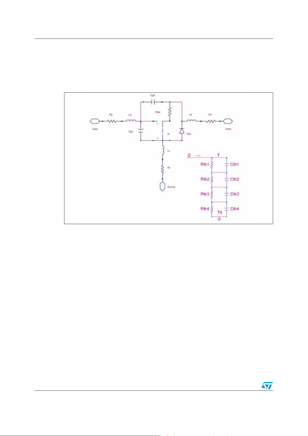
Figure 1. Model schematic
By observing the equivalent model schematic of Figure 1, the following elements can be
noted:
● Parasitic elements associated with the device
● Nonlinear current generator
● JFET resistance
● Substrate-body diode
Parasitic elements
To model the parasitic elements of the device, a resistor and an inductor are place d in series
at each terminal. The model can change the resistance and inductance v alu es accord ing to
the simulation temperature.
Parameter P in Equation 1 is the temperature dependence, where T
coefficient, T is the temperature used in the simu lation and Tnom is the temper ature used to
measure the parameter value.
Equation 1
PT() PT
()1TCTT
NOM
–()⋅+()⋅=
NOM
is its temperature
c
4/18
Page 5

AN2657 Model description and parameter extraction
Nonlinear current generator
The nonlinear current generat or controlled by Vgs and Vds is the most important factor used
to calculate the static and dynamic current of the device. Moreover, the static current is
required to define the working region of the MOS.
Table 1. Parameters required for the extraction of the current generator equations
Name Description
VT0 Threshold voltage [V]
ETA Drain induce barrier lowering (DIBL) [V-1]
-2
KP0 Transconduttance [A*V
THETA Mobility degradation [V
VGTHETA Mobility degradation exponent [-]
THETA2..9 From 2nd to 9th degradation polynomial factor [V
XN Slope subthreshold current [V
DEL Body effect linearization coefficient [-]
DELVG Body effect linearization coefficient independent of Vgs [V-1]
L0 Critical length [m]
L Channel length [m]
]
-VGTHETA
]
-2
]
-1
]
EPS Output conductance factor if L0>L [m]
KE Output conductance factor if L0<L [Vm]
DT_KP Mobility thermal coefficient [-]
-1
DT_VT Thermal coefficient of threshold voltage [°C
]
Table 1 reports all the parameters required to extract the equat ions of th e current ge nerat or.
To get the generator current equation, a set of equations must be defined. An important
parameter to consider is the threshold voltage of the device shown in Equation 2.
Equation 2
V
THVT0
η VDSDVVT T T
-
–()⋅+⋅–=
NOM
Moreover, a new threshold voltage formula is necessary to describe the weak and strong
inversion region in a single equation (Equation 3).
Equation 3
VR V
2XNU
TH
U
TH
⋅⋅–=
KT⋅
--------------=
TH
q
To describe both reg io ns, a new gate voltage can be defined as in Equation 4.
Equation 4
⎧
⎪
V
VTH2XNUTHe
=
⎨
gg
⎪
⎩
⋅⋅⋅+
V
gs
VgsVR–
------------------------------------ -
2XNU
⋅⋅
TH
5/18
Page 6

Model description and parameter extraction AN2657
Equation 5
KP KP0
T ° K()
⎛⎞
--------------------------- -
⋅=
⎝⎠
T
NOM
DTKP
° K()
-
Another important parameter to define is the gain factor with zero bias . Referring to
Equation 5, 6 and 7, the gain factor degrades according to the V
voltage (mobility
gs
degradation). Equation 8 and 9, which define the drain satu ration voltage, complete the set
of equations needed to define the generator current (Equation 10 and 11).
Equation 6
FV
()
gst
⎧
⎪
⎪
=
⎨
1TV
⎪
⎪
⎩
vgT
gst
1
9
+⋅+
∑
I2=
TIV
⋅
I
gst
0≤
V
gst
0>
V
gst
Equation 7
KP
EFF
------------------- -=
()
FV
gst
KP
Equation 8
Equation 9
Equation 10
I
DS
Equation 11
AL0
B
CKEL
δ∆∆VG Vgg⋅+=
D
1
D
2
KP
⎧
EFF
⎪
=
⎨
⎪
⎩
IDSS KP
2L2
–=
L
-- -
L02⋅=
δ
3
⋅=
BA–()Vgg VTH–()C1δ–()⋅–⋅=
2
D
4C VggV
1
VDSAT
Vds V( gg VTH– 0.05 Vds 1 ∆+())⋅⋅–⋅⋅
IDSS 1 A
⎛⎞
⋅
⎝⎠
VDSAT Vgg VTH– 0.5 VDSAT 1 ∆+()⋅⋅–()⋅⋅=
EFF
δ∆∆VG Vgg⋅+=
–()1 δ+()0.5 A B–⋅()⋅⋅ ⋅ ⋅–=
TH
D
----------------------------------------------------- -=
1 δ+()2BA–⋅()⋅
Vds VDSAT–
------------------------------------------ -
⋅+
BVDSATC+⋅
2D1
+
VDSAT<
V
DS
V
VDSAT≥
DS
The automatic ADS optimizer was used to extract the parameters for the current gener ator.
The threshold voltage and the gain f a ctor ha v e been e xt racted from th e input char acteristics
with Vds at a low voltage level. Concerning mobility degradation, the transconductance
parameter was used varying Vds and with Vgs at a high voltage level. The sub-threshold
voltage was extracted from the input characteristics with a gate voltage lev el below the
threshold voltage level.
6/18
Page 7

AN2657 Model description and parameter extraction
L is the physical channel length of the MOS, while L0 influences the output conductance
which depends on KE and EPS. DEL and DELVG affect the VDSAT and are extracted from
the output characteristics in the satura tion region. As mentioned pre viously, all the equations
have been implemented in verilog language.
JFET resistance
The quasi-saturation region is modeled by a nonlinear JFET resistor. The mathematical
empirical equation is defined in Equation 12, where pres depends on t he current and on the
drop voltage across R
Equation 12
.
j
RjfVds Vgs,()gpres()hT()⋅⋅=
Figure 2. R
vs. Vds
jfet
Useful to delete any convergence problem, Figure 2 shows the resistor law for the variation
of Vds (using the right hand function approach) (Equation 13). A similar graph and function
can be obtained by v arying Vgs [3].
Equation 13
Vds VDI–
----------------------------
RjVds()RI0 SR FSI Log10110
⎛⎞
+
⎜⎟
⎝⎠
FSI
FSF Log
⋅–⋅⋅+=
10
Vds VDF–
------------------------------
⎛⎞
110
⎜⎟
⎝⎠
FSF
+
The function g(pres) was created to bind the Rj to the current Id. This is accomplished by
introducing a new parameter link ed to the dissipated po we r on R
(Equation 14), where pres
j
is linked to the dissipated power on Rj through RPWR.
Equation 14
gpres()1 PCR1 PCR2 pres⋅+()pres⋅+=
h(T) (Equation 15), introduces the temperature dependence of R
, where TCR1 and TCR2
j
are temperature coefficients in the linear region.
R
is extracted from the DC output characteristics in the linear region with high bias current.
j
7/18
Page 8

Model description and parameter extraction AN2657
Equation 15
hT() 1TT
–()TCR1 T T
NOM
–()TCR2⋅+()⋅+=
NOM
Substrate-body diode
The body-substrate diode is emplo yed to describe the breakdo wn, the drain current leakage
and the capacitance between the dr ain and source.
The thermal variations are shown by Equation 16.
Equation 16
CjT CJ 1 T+ CCJ T T
VjT VJ 1 T+ CVJ T T
CjkparT CJPAR 1 T+ CCJPAT T T
-
-
BVT BV 1 TCBV T T
BVVGT BVVG 1 TCBVVG T T
R
LEAKT
R
LEAK
-
-
-
1( TCR
-
-
To include the temperature in the saturation current refer to Equation 17.
Equation 17
XTI
T
---------------
T
NOM
----------
N
exp⋅⋅
dIs
⎛⎞
--------
⎝⎠
dT
T200
qEG⋅
⎛⎞
-------------------
⎝⎠
K
T ° K()T200–()⋅+
IsT
⎧
⎛⎞
⎪
IS
⎝⎠
⎪
+=
⎨
⎪
⎪
Is200
⎩
–()⋅()⋅=
NOM
–()⋅()⋅=
NOM
-
-
–()⋅()⋅=
–()⋅+()⋅=
NOM
–()⋅+()⋅=
TT
LEAK
⋅
–())⋅+⋅=
NOM
1
⎛⎞
---------------
⎝⎠
T
NOM
NOM
1
---–
T
NOM
T 200≤
T 200>
°C
°C
The diode current is implemented in Equation 18, 19, 20, 21 and 22. The cha rge equation is
given by Equation 23.
Equation 18
Id
⎧
⎛⎞
IsT
⋅
⎪
=
⎝⎠
⎨
⎪
Ir1 Ir2 Ir3++
⎩
Vd
⎛⎞
-----------------
⎝⎠
NVt⋅
1–exp
Equation 19
Vd
⎛⎞
Ir1 IsT
-----------------
⎝⎠
NVt⋅
1–exp⋅=
Equation 20
Ir2
Vd
--------------------=
R
LEAKT
Equation 21
Vd BVT BVVGT Vgs⋅++
Ir3 Vd()Ibv
⎛⎞
exp⋅⋅sgn=
------------------------------------------------------------------------–
⎝⎠
NBV Vt⋅
8/18
Page 9

AN2657 Model description and parameter extraction
Equation 22
I
Ibv
⎧
BV
⎪
=
BV
⎨
------- -
I
⋅
⎪
s
V
T
⎩
0A>
I
BV
0A≤
I
BV
Equation 23
⎧⎫
⎪⎪
⎪⎪
⎪⎪
Qd TT Id f1 1
⎪⎪
⎪⎪
⎪⎪
⎨⎬
⎪⎪
⎪⎪
⎪⎪
⎪⎪
⎪⎪
⎪⎪
Qd TT Id f1 f2 Vd 0.5
⎩⎭
f1
f2 1 FCP 1 MJ+()⋅–=
⎛⎞
⎝⎠
CjT VjT⋅
f1
-------------------------- -=
1MJ–
VjT
CjT
1MJ–()
1MJ–()
⋅
MJ Vd
------------------------- -
⋅+⋅
VjT
CjlparT Vd⋅+⋅+⋅=
-
2
CjlparT Vd⋅+⋅+⋅=
-
1Vd–
⎛⎞
⎛⎞
---------------- -
+
⎝⎠
⎝⎠
--------------------------------------------=
1FCP–()
VDFCP≤
V
D
FCP>
The remaining model parameters are the capacita n ces Cgs an d Cg d of th e MO SF ET. The
gate-source capacitance is modeled with a constant capacitance, because it is related to a
highly doped MOSFET (Equation 24).
Equation 24
Qgs CgsT Vgs⋅=
Moreover, the gate-drain capacitance can be considered as a classic MOSFET model
capacitance, where the equation s of th e charged capacit ance (Eq uation 25 , 26, 27, 28) can
be divided into four r egions (Figure 3). Even in this case, capacitance variation depe nds on
temperature (Equation 29).
Equation 25
Cgx0
---------------------------------------------------- CgdovlT+=
Vgx VFB–
⎛⎞
1
---------------------------- -–
⎝⎠
Vjx
⎛⎞
1
–
⎝⎠
VFB Vgx–
---------------------------- -+
Vjx
Mjx
1Mjx–
CgdovlT Vgd⋅+⋅=
Qgd
Cgx0 Vjx⋅
------------------------------ -
1Mjx–
Cgd
1Mjx–
VFB
⎛⎞
⎛⎞
1
----------- -+
⎝⎠
⎝⎠
Vjx
Equation 26
Cgx0 Vjx⋅
Qgd Cgx0 Vgd VFB–()
------------------------------ -
1Mjx–
⎛⎞
⎛⎞
1
⎝⎠
⎝⎠
VFB
----------- -+
Vjx
1Mjx–
1–
CgdovlT Vgd⋅+⋅+⋅=
Equation 27
Cgx0
---------------------------------------------------- CgdovlT+=
Vgx VFB–
⎛⎞
1
---------------------------- -–
⎝⎠
Vjx
VFB Vgx–
⎛⎞
⎛⎞
1
---------------------------- -+
⎝⎠
⎝⎠
Vjx
Mjx
1Mjx–
1–
CgdovlT Vgd⋅+⋅+⋅=
Qgd Cgx0 VFB
Cgd
Cgx0 Vjx⋅
------------------------------ -
1Mjx–
Equation 28
Cgd Cgx0 CgdovlT+=
Qgd Cgx0 CgdovlT+()Vgd⋅=
9/18
Page 10

Model description and parameter extraction AN2657
2
Equation 29
GgxT CGX0 1 CGXTC1 T T
VfbT VFB 1 VFBTC1X T T
CgdovlT CGDOVL 1 CGDOVLTC T T
–()CGXTC2 T T
NOM
–()⋅+()⋅=
NOM
–()⋅+()⋅=
–()
⋅+⋅+()⋅=
NOM
NOM
Figure 3. Gate-drain charge variation vs. Vds
To extract the capacitance variables, a classic configuration has been used to measure the
C
, C
iss
oss
and C
rss
.
Thermal node
A "thermal node" has been introduced to consider the self-heating effect (Figure 1).
The voltage between the external thermal circuit port and the source node is related to the
junction temperature rise. The current source of the circuit is equal to the dissipated power
[4] [5]. In this first model implementation we have not considered the temperature
dependent variables.
Package simulation
To include all the parasitic elements of the package in the model, several electromagnetic
simulations were performed [6].
10/18
Page 11

AN2657 Model description and parameter extraction
Figure 4. Generic internal RF package structure
Figure 5. PowerFLAT cross-section
The molding resin has a dielectric constant equal to 4 a nd a dielect ric loss tangent of 0.005.
The leads of the package are made of copper, while the bonding wires are made of gold.
During the simulation, the device contact pads and the paddle are considered as a PEC
(perfect electric conductive surface lossless). Instead, along the external sides of the air bo x
containing the package, an electric and magnetic field total wave absorption condition was
set to consider the radiation losses (Equation 30).
Equation 30
∇ E×()
tan
jk
0
j
-----
∇
k
0
tan
∇
tan
E
×()×
tan
j
-----
∇
k
0
tan
∇
tan
E
⋅()×⋅+⋅–⋅=
tan
During the simulation lumped ports were used to excite the fields (Figure 6) [7]. The
package simulation performed was in the frequency range from 1 MHz to 50 GHz.
11/18
Page 12

Model description and parameter extraction AN2657
eq, G
Figure 6. Simulated version of the PowerFLAT
To minimize the simulation time and increase accur acy, the structure was split into two parts
(drain and gate). In this way, the reciprocal coupling between the input and output parts are
not considered. To take into account such effect, an extra capacitor (Cgd-package) has
been used. To complete the package model an extra inductor (Lvia) associated with the
source has been added. This inductor represents the effect created by the "via holes"[8] [9].
The S-parameters concerning the electromagnetic simulation of the gate section of the
package are shown in Figure 7.
Figure 7. S-parameters of the simulated package
Input Ref lection Coeffic ient
S(1,1)
S(2,2)
freq (1.000MHz to 50.00GHz)
2
0
-2
-4
-6
-8
dB(S(2,1))
-10
-12
-14
-16
Forward T ransmission, dB
5 1015202530354045050
freq, GHz
200
150
100
50
0
-50
phase(S(2,1))
-100
-150
-200
Forward T ransmission, phase
5 1015202530354045050
fr
Hz
Moreover, using the measured S-parameters of the packaged device, it was possible to
extract the Cgd-package and the Lvia. Observing Figure 8, it is possible to see the circuit
representing the union between the package model and the device model.
12/18
Page 13

AN2657 Model description and parameter extraction
Figure 8. Overall model schematic
DC and RF small signal validation
Figure 9, 10, and 11 compare the measured DC and RF small signal parameters with the
simulated parameters (C
curves). The simulations predict with good app ro ximat ion the abo v e mentioned p ara meters ,
including S21 and S22 which are the most difficult to predict.
iss
, C
oss
, C
, low signal S-parameters, and input and output DC
rss
Figure 9. Measured C
iss
, C
oss
, C
vs. simulated parameters
rss
13/18
Page 14

Model description and parameter extraction AN2657
I
fficient
O
fficient
Figure 10. Measured S-parameters vs. simulated parameters (Vds= 7.2 V;
Idq= 100 mA)
S(1,1)
nput Reflection Coe
S(1,2)
S(3,4)
-0.04
-0.03
-0.05
Rev er se Tr ansmission
-0.02
-0.01
0.00
0.01
0.02
0.03
0.04
0.05
freq (1.000MHz t o 3.000GHz)
Forwar d Transmission
-60 -40 -20 0 20 40 60-80 80
S(2,1)
S(4,3)
freq ( 1. 0 00MHz t o 3.000GHz)
freq (1.000MHz to 3.00 0GHz)
utput ReflectionCoe
S(2,2)
freq (1.000MHz to 3.00 0GHz)
Figure 11. Measured input and output DC curves vs. simulated curves
14/18
Page 15

AN2657 Model description and parameter extraction
Large signal validation
Using the ADS with harmonic balance engine simulator [10], the model has been simulated
in conjunction with the DC network and the input and output matching network of ST's
demonstration board DB-54003L-175 (Figure 12).
The DB-54003L-175 demonstration board was developed to demonstrate the best
broadband performance of PD54003L-E.
Figure 12. DB-54003L-175 demoboard
In the harmonic balance simulations we used all the information relative to the board and the
S-parameters of the lumped capacitors and inductors. Figure 13 compares the simulations
and measurements of the demonstration boar d at 155 MHz, varying the power delive re d by
the generator at the input port.
P
is the power available from the generator, Nd is the drain efficiency, IRL (input return
IN
loss) is the ratio between the power reflected from the device and the power available from
the generator , and G ain is the ratio be tween the p ower dissipated on the load an d the pow er
available from the generator.
Figure 13. Measured RF demonstration board performance vs simulated
performance
15/18
Page 16

Conclusions AN2657
2 Conclusions
Thanks to this new verilog model, customers will now be able to predict and simulate the
behavior of STMicroelectronics' RF DMOS and LDMOS products, reducing design cycle
time and time-to-market.
3 References
1. "Beha vioral Modeling with the verilog-a Language," Springer, Oct. 1997.
2. "Behavioral Modeling of Nonlinear RF and Microwave Devices," Artech House
Publishers, Nov. 1999.
3. "Lumped Element Behavioural High Voltage MOS Model," Mixed Design of Integrated
Circuits and System, 2006. MIXDES 2006. Proceedings of the International
Conference, June 2006.
4. "Analysis and Simulation of Self-Heating Effects on RF L DMOS Devices ," Simulation of
Semiconductor Processes and Devices , 2005. SISPAD 2005. International Conference
on, Sept. 2005.
5. "New LDMOS Model Delivers Powerful Transistor Library - The CMC Model,"
www. highfrequencyelectronics.com, Oct. 2004.
6. "User's guide - high frequency structure simulator," Ansoft.
7. "Port tutorial series - high frequency structure simulator," Ansoft.
8. "RF package characterization and modeling," University/ Government/Industry
Microelectronics Symposium, 1999. Proceedings of the Thi rteenth Biennial, June 1999.
9. "Electrical modeling of rfic packages up to 12 ghz," Electronic Components and
Technology Conference, June 1999.
10. "Guide to Harmonic Balance Simulation in ADS," Agilent.
16/18
Page 17

AN2657 Revision history
4 Revision history
Table 2. Document revision history
Date Revision Changes
27-Nov-2007 1 Initial release
17/18
Page 18

AN2657
Please Read Carefully:
Information in this document is provided solely in connection with ST products. STMicroelectronics NV and its subsidiaries (“ST”) reserve the
right to make changes, corrections, modifications or improvements, to this document, and the products and services described herein at any
time, without notice.
All ST products are sold pursuant to ST’s terms and conditions of sale.
Purchasers are solely res ponsibl e fo r the c hoic e, se lecti on an d use o f the S T prod ucts and s ervi ces d escr ibed he rein , and ST as sumes no
liability whatsoever relati ng to the choice, selection or use of the S T products and services described herein.
No license, express or implied, by estoppel or otherwise, to any intellectual property rights is granted under this document. If any part of this
document refers to any third pa rty p ro duc ts or se rv ices it sh all n ot be deem ed a lice ns e gr ant by ST fo r t he use of su ch thi r d party products
or services, or any intellectua l property c ontained the rein or consi dered as a warr anty coverin g the use in any manner whats oever of suc h
third party products or servi ces or any intellectual property contained therein.
UNLESS OTHERWISE SET FORTH IN ST’S TERMS AND CONDITIONS OF SALE ST DISCLAIMS ANY EXPRESS OR IMPLIED
WARRANTY WITH RESPECT TO THE USE AND/OR SALE OF ST PRODUCTS INCLUDING WITHOUT LIMITATION IMPLIED
WARRANTIES OF MERCHANTABILITY, FITNESS FOR A PARTICUL AR PURPOS E (AND THEIR EQUIVALE NTS UNDER THE LAWS
OF ANY JURISDICTION), OR INFRINGEMENT OF ANY PATENT, COPYRIGHT OR OTHER INTELLECTUAL PROPERTY RIGHT.
UNLESS EXPRESSLY APPROVED IN WRITING BY AN AUTHORIZED ST REPRESENTATIVE, ST PRODUCTS ARE NOT
RECOMMENDED, AUTHORIZED OR WARRANTED FOR USE IN MILITARY, AIR CRAFT, SPACE, LIFE SAVING, OR LIFE SUSTAINING
APPLICATIONS, NOR IN PRODUCTS OR SYSTEMS WHERE FAILURE OR MALFUNCTION MAY RESULT IN PERSONAL INJ URY,
DEATH, OR SEVERE PROPERTY OR ENVIRONMENTAL DAMAGE. ST PRODUCTS WHICH ARE NOT SPECIFIED AS "AUTOMOTIVE
GRADE" MAY ONLY BE USED IN AUTOMOTIVE APPLICATIONS AT USER’S OWN RISK.
Resale of ST products with provisions different from the statements and/or technical features set forth in this document shall immediately void
any warranty granted by ST fo r the ST pro duct or serv ice describe d herein and shall not cr eate or exten d in any manne r whatsoever , any
liability of ST.
ST and the ST logo are trademarks or registered trademarks of ST in various countries.
Information in this document su persedes and replaces all informatio n previously supplied.
The ST logo is a registered trademark of STMicroelectronics. All other names are the property of their respective owners.
© 2007 STMicroelectronics - All rights reserved
STMicroelectronics group of compan ie s
Australia - Belgium - Brazil - Canada - China - Czech Republic - Finland - France - Germ any - Hong Kong - India - Israel - Italy - Japan -
Malaysia - Malta - Morocco - Singapore - Spain - Sweden - Switzerland - United Kingdom - United States of America
www.st.com
18/18
 Loading...