

Page 1
AN2656
Application note
STM32F10xxx
LCD glass driver firmware
Introduction
This application note describes a technique for driving liquid crystal displays (LCD) with
STM32F10xxx microcontrollers (MCU), that is without any specific on-chip LCD driver
hardware. This technique offers a solution for applications that require a display at low cost
together with the versatile capabilities of standard STM32F10xxx MCUs. This application
note also provides a technique to control the LCD contrast through firmware.
After an introduction on LCDs, Section 1, Section 2 & Section 3 describe the typical
waveforms required to drive an LCD with a multiplexing rate of 1 or 2 (duplex) and 4
(quadruplex). Section 3 presents a solution based on a standard STM32F10xxx MCU
directly driving a quadruplex LCD. This solution can be implemented with any
STM32F10xxx MCU as it only requires the standard I/O ports and one timer, which are
standard features on all STM32F10xxx MCUs. Section 4 describes how to use the
STM32F10xxx LCD glass library and gives a brief presentation of the LCD glass demo.
Section 5 describes low-power management using the LCD glass, and gives current and
load CPU measurements. Finally, Section 7 gives an example of the LCD connections to the
STM32 MCU (two types of LCDs: 4 digits (64 segments: ref CT4-098-LV) and 8 digits (128
segments: ref: PD-878).
With the STM32F10xxx LCD glass library, the CPU load for controlling the LCD is around
0.05% (at 72 MHz), and the number of external components is kept to the minimum (two
external resistors per COM line). The number of I/Os involved is the same as in solutions
using an on-chip LCD hardware driver or an external hardware LCD driver. With firmware
contrast control, the STM32F10xxx MCU offers a very flexible solution that can be adapted
easily to a range of applications.
The measured DC value depends on the used resistors (refer to Section 3) and the user
configuration: LCD interruption priority configuration (refer to Section 4.2).
April 2009 Doc ID 14144 Rev 2 1/33
www.st.com
Page 2

Contents AN2656
Contents
1 LCD principle . . . . . . . . . . . . . . . . . . . . . . . . . . . . . . . . . . . . . . . . . . . . . . . 5
2 LCD drive signals . . . . . . . . . . . . . . . . . . . . . . . . . . . . . . . . . . . . . . . . . . . 7
2.1 Single backplane LCD drive . . . . . . . . . . . . . . . . . . . . . . . . . . . . . . . . . . . . 7
2.2 Duplexed LCD drive . . . . . . . . . . . . . . . . . . . . . . . . . . . . . . . . . . . . . . . . . . 7
2.3 Quadruplex LCD drive . . . . . . . . . . . . . . . . . . . . . . . . . . . . . . . . . . . . . . . . 9
2.3.1 LCD mean voltage calculation . . . . . . . . . . . . . . . . . . . . . . . . . . . . . . . . 11
2.3.2 Contrast calculation . . . . . . . . . . . . . . . . . . . . . . . . . . . . . . . . . . . . . . . . 11
3 Example of a quadruplex LCD with STM32F10xxx . . . . . . . . . . . . . . . 13
4 Firmware description . . . . . . . . . . . . . . . . . . . . . . . . . . . . . . . . . . . . . . . 17
4.1 How to use the LCD library . . . . . . . . . . . . . . . . . . . . . . . . . . . . . . . . . . . 18
4.1.1 How to select the LCD glass by firmware . . . . . . . . . . . . . . . . . . . . . . . 18
4.1.2 How to select GPIOs to connect the LCD glass to STM32F10xxx . . . . 18
4.1.3 How to select the timer interrupt priority that drives the LCD . . . . . . . . 20
4.1.4 LCD contrast control . . . . . . . . . . . . . . . . . . . . . . . . . . . . . . . . . . . . . . . 21
4.2 LCD timer interrupt . . . . . . . . . . . . . . . . . . . . . . . . . . . . . . . . . . . . . . . . . . 21
4.2.1 LCD with high interrupt priority . . . . . . . . . . . . . . . . . . . . . . . . . . . . . . . 21
4.2.2 LCD with low-high interrupt priority (using boosting priority) . . . . . . . . . 22
4.2.3 LCD interrupt always with lowest priority . . . . . . . . . . . . . . . . . . . . . . . . 23
4.3 Default demo configurations . . . . . . . . . . . . . . . . . . . . . . . . . . . . . . . . . . . 23
5 LCD glass in battery-powered and low-power applications . . . . . . . . 24
5.1 Hardware implementation . . . . . . . . . . . . . . . . . . . . . . . . . . . . . . . . . . . . 24
5.2 LCD glass managed by the timer using the Sleep low-power
mode . . . . . . . . . . . . . . . . . . . . . . . . . . . . . . . . . . . . . . . . . . . . . . . . . . . . 25
5.2.1 Some current and CPU load measurements . . . . . . . . . . . . . . . . . . . . . 25
5.3 LCD glass managed by the RTC and using the Stop low-
power mode . . . . . . . . . . . . . . . . . . . . . . . . . . . . . . . . . . . . . . . . . . . . . . . 26
5.3.1 Some current and CPU load measurements . . . . . . . . . . . . . . . . . . . . . 27
6 Comparison of the timer and RTC methods . . . . . . . . . . . . . . . . . . . . . 29
6.1 Timer method . . . . . . . . . . . . . . . . . . . . . . . . . . . . . . . . . . . . . . . . . . . . . . 29
2/33 Doc ID 14144 Rev 2
Page 3

AN2656 Contents
6.2 RTC method . . . . . . . . . . . . . . . . . . . . . . . . . . . . . . . . . . . . . . . . . . . . . . . 29
7 Hardware implementation . . . . . . . . . . . . . . . . . . . . . . . . . . . . . . . . . . . 30
7.1 Schematic . . . . . . . . . . . . . . . . . . . . . . . . . . . . . . . . . . . . . . . . . . . . . . . . . 30
7.2 LCD segment line connections . . . . . . . . . . . . . . . . . . . . . . . . . . . . . . . . . 31
8 Revision history . . . . . . . . . . . . . . . . . . . . . . . . . . . . . . . . . . . . . . . . . . . 32
Doc ID 14144 Rev 2 3/33
Page 4

List of figures AN2656
List of figures
Figure 1. LCD principle . . . . . . . . . . . . . . . . . . . . . . . . . . . . . . . . . . . . . . . . . . . . . . . . . . . . . . . . . . . . 5
Figure 2. Equivalent electrical schematic of an LCD segment. . . . . . . . . . . . . . . . . . . . . . . . . . . . . . . 6
Figure 3. LCD signals for direct drive. . . . . . . . . . . . . . . . . . . . . . . . . . . . . . . . . . . . . . . . . . . . . . . . . . 7
Figure 4. Basic LCD segment connection in duplexed mode . . . . . . . . . . . . . . . . . . . . . . . . . . . . . . . 8
Figure 5. LCD signals for duplexed mode . . . . . . . . . . . . . . . . . . . . . . . . . . . . . . . . . . . . . . . . . . . . . . 8
Figure 6. Basic LCD segment connection in quadruplexed mode . . . . . . . . . . . . . . . . . . . . . . . . . . . . 9
Figure 7. LCD timing diagram for quadruplex mode . . . . . . . . . . . . . . . . . . . . . . . . . . . . . . . . . . . . . 10
Figure 8. LCD timing diagram for a single segment. . . . . . . . . . . . . . . . . . . . . . . . . . . . . . . . . . . . . . 11
Figure 9. Hardware connection diagram (1/2 bias control) . . . . . . . . . . . . . . . . . . . . . . . . . . . . . . . . 13
Figure 10. LCD timing diagram with active and dead time (to decrease Vrms). . . . . . . . . . . . . . . . . . 14
Figure 11. LCD timing diagram with active and dead time (to increase Vrms) . . . . . . . . . . . . . . . . . . 15
Figure 12. Screenshot of Vcom3 and Vsegx (Segment1 of digit2) . . . . . . . . . . . . . . . . . . . . . . . . . . . 16
Figure 13. Screenshot of the four common lines . . . . . . . . . . . . . . . . . . . . . . . . . . . . . . . . . . . . . . . . 16
Figure 14. Timing used by the STM32F10xxx LCD library . . . . . . . . . . . . . . . . . . . . . . . . . . . . . . . . . 17
Figure 15. LCD timing diagram for a single segment. . . . . . . . . . . . . . . . . . . . . . . . . . . . . . . . . . . . . . 19
Figure 16. Hardware connection diagram (1/2 bias control) . . . . . . . . . . . . . . . . . . . . . . . . . . . . . . . . 24
Figure 17. Timer method state machine . . . . . . . . . . . . . . . . . . . . . . . . . . . . . . . . . . . . . . . . . . . . . . . 25
Figure 18. Timer method chronogram (in this case duty cycle = 50%) . . . . . . . . . . . . . . . . . . . . . . . . 26
Figure 19. RTC method state machine . . . . . . . . . . . . . . . . . . . . . . . . . . . . . . . . . . . . . . . . . . . . . . . . 27
Figure 20. RTC method chronogram . . . . . . . . . . . . . . . . . . . . . . . . . . . . . . . . . . . . . . . . . . . . . . . . . . 28
Figure 21. LCD - STM32F10xxx connection example . . . . . . . . . . . . . . . . . . . . . . . . . . . . . . . . . . . . . 30
4/33 Doc ID 14144 Rev 2
Page 5
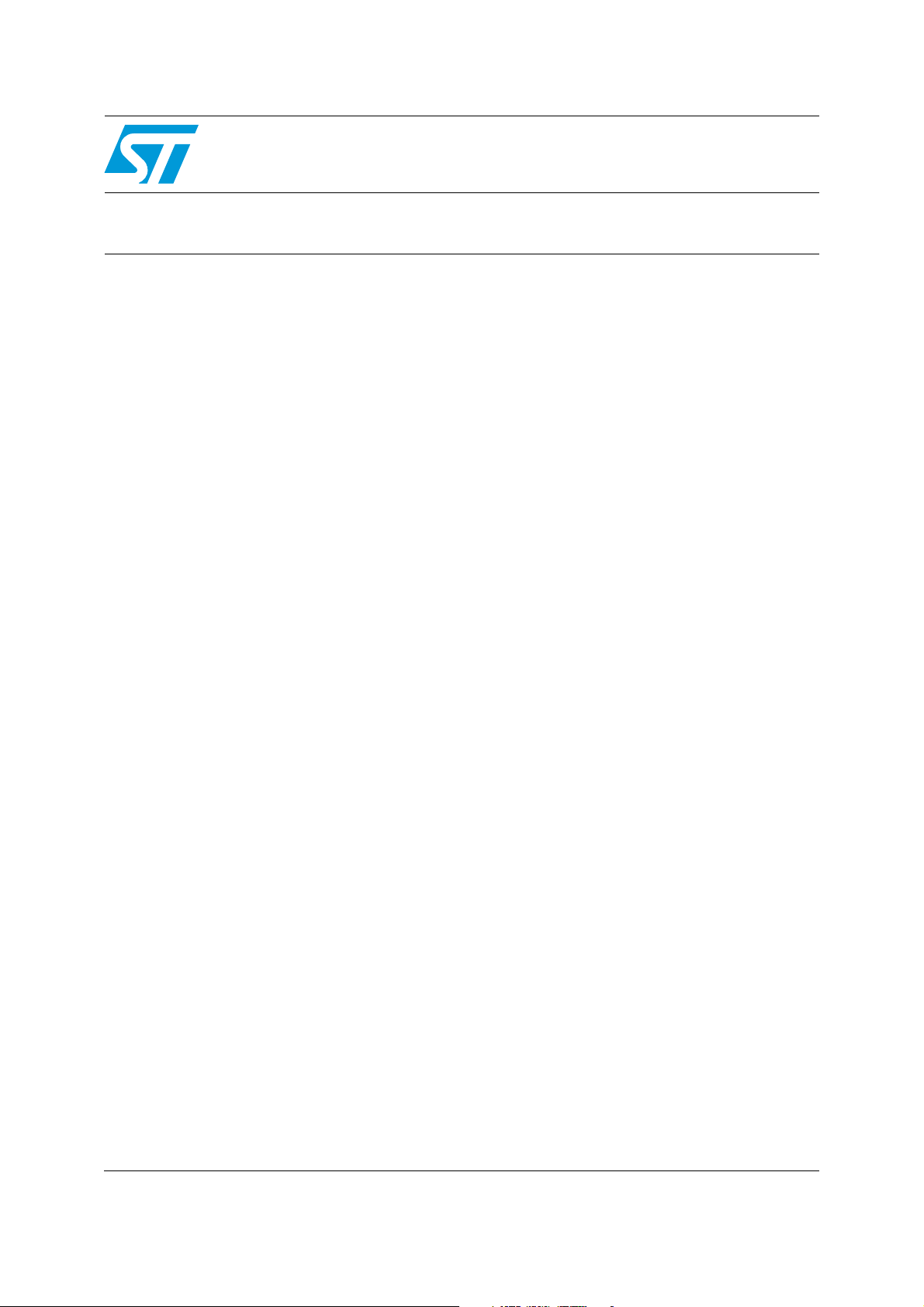
AN2656 LCD principle
Mean Signal
2
1 LCD principle
Figure 1. LCD principle
An LCD panel is composed of many layers. A liquid crystal is filled between two of them
(glass plates), that are separated by thin spacers coated with transparent electrodes and
orientation layers. The orientation layer usually consists of a polymer (e.g. polyimide) that
has been unidirectionally rubbed using, for instance, a soft cloth. As a result, the liquid
crystal molecules are fixed, with their alignment more or less parallel to the plates, in the
direction of rubbing. The crystal alignment directions at the surface of the two plates are
perpendicular so that the molecules between the two plates undergo a homogeneous twist
deformation in alignment to form a helix.
If no electric field is applied, the birefringent liquid crystal molecules keep their helical
structure and rotate linearly polarized light waves passing through the plates. The
transmitted light wave is then allowed through a crossed exit polarizer. As a result, the
modulator has a bright appearance.
On the other hand, if an AC voltage of a few volts is applied, the resulting electric field forces
the liquid crystal molecules to align themselves along the field direction and the twist
deformation (the helix) is unwound. In this case, the polarization of the incident light is not
rotated by the crystal molecules and the crossed exit polarizer blocks the light wave. As a
result, the modulator appears dark.
The inverse switching behavior can be obtained with parallel polarizers. It must also be
noted that gray scale modulation is easily achieved by varying the voltage between the
crystal molecule reorientation threshold (reorientation is resisted by the elastic properties of
liquid crystals) and the saturation field.
LCDs are sensitive to root mean square voltage (Vrms= ) levels. With a low
root mean square voltage applied to it, an LCD is practically transparent (the LCD segment
is then inactive or off). To turn an LCD segment on, causing the segment to turn dark (from
light gray to opaque black), an LCD RMS voltage greater than the LCD threshold voltage is
applied to the LCD. The LCD RMS voltage is the RMS voltage across the capacitor C in
Figure 2, which is equal to the potential difference between the SEG and COM values.
The LCD threshold voltage depends on the quality of the liquid used in the LCD and the
temperature. The optical contrast is defined by the difference in transparency of an LCD
segment that is on (dark) and an LCD segment that is off (transparent). The optical contrast
depends on the difference between the RMS voltage on an on segment (V
voltage on an off segment (V
V
(rms), the higher the optical contrast. The optical contrast also depends on the level of
OFF
V
versus the LCD threshold voltage. If VON is below or close to the threshold voltage, the
ON
LCD is completely or almost transparent. If V
). The higher the difference between VON(rms) and
OFF
is close or above the threshold voltage, the
OFF
) and the RMS
ON
LCD is completely black.
Doc ID 14144 Rev 2 5/33
Page 6
LCD principle AN2656
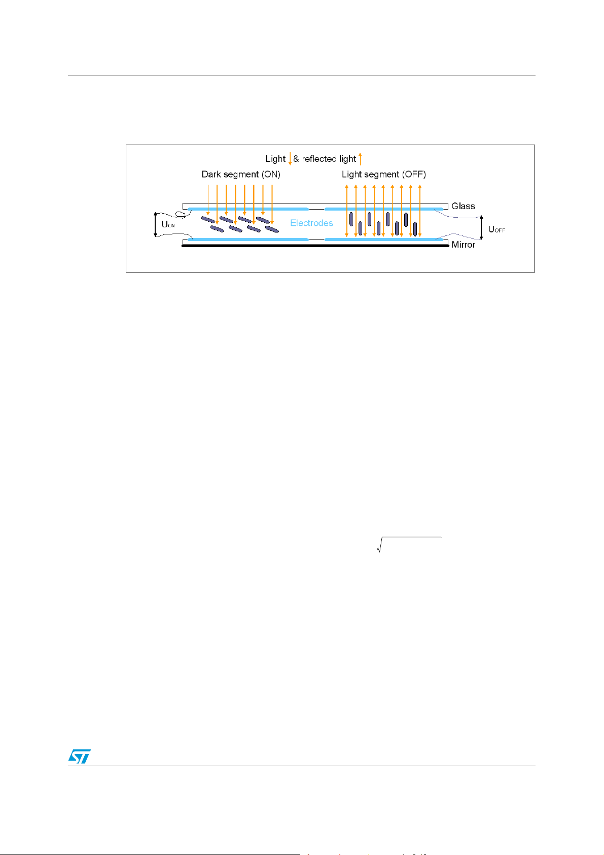
C
R
S
S
COM
ai14758
In this document, contrast is defined as D = VON(rms) / V
OFF
(rms).
The applied LCD voltage must also alternate to give a zero DC value to prevent the
electrolytic process and so, ensure a long LCD lifetime.
The higher the multiplexing rates, the lower the contrast. The signal period also has to be
short enough to avoid visible flickering on the display.
Figure 2. Equivalent electrical schematic of an LCD segment
Note: The DC value should never be more than 100 mV (refer to the LCD manufacturer’s
datasheet), otherwise the LCD lifetime may be shortened. The frequency range is 30 Hz to
200 Hz typically. If it is less, the LCD flickers, if it is greater, power consumption increases.
6/33 Doc ID 14144 Rev 2
Page 7
AN2656 LCD drive signals
COM
ai14759
+V
DD
S
+V
DD
+V
DD
S1 = COM – S
OFF
S
+V
DD
+V
DD
S1 = COM – S
–V
DD
ON
2 LCD drive signals
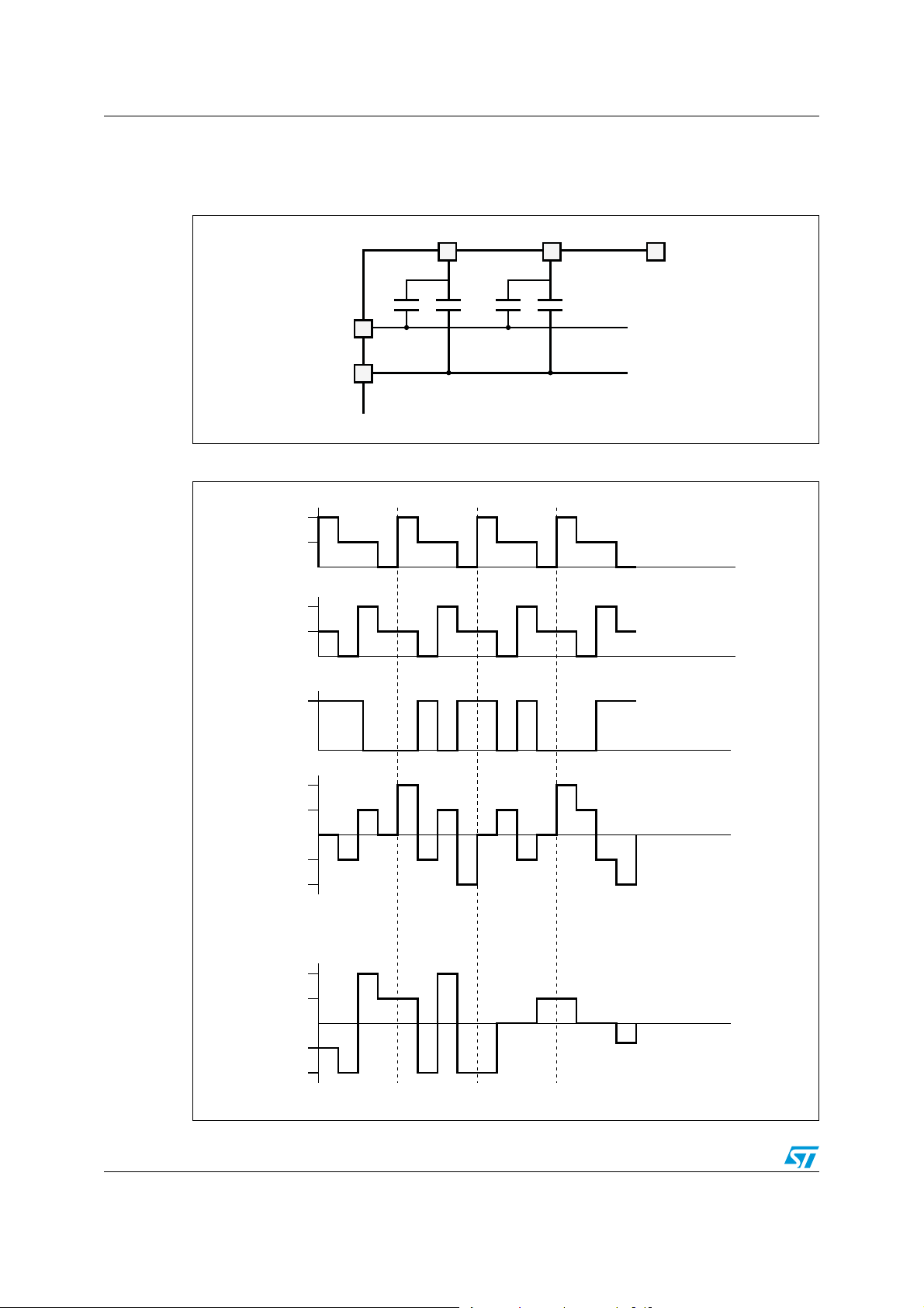
2.1 Single backplane LCD drive
In a single backplane drive, each LCD segment is connected to a segment line (Sx) and to a
backplane (common line) common to all the segments. A display using S segments is driven
with S+1 MCU output lines. The backplane is driven with a COM signal between 0 and V
with a duty cycle of 50%.
When switching a segment on, a signal with opposite polarity to COM is sent to the
corresponding Segment pin. When the noninverted COM signal is sent to the Segment pin,
the segment is off. Using an MCU, the I/O operates in output mode at either logic 0 or 1.
Figure 3. LCD signals for direct drive
DD
2.2 Duplexed LCD drive
In a duplexed drive, two backplanes are used instead of one. Each LCD segment line (Sx) is
connected to two LCD segments, whose other side is connected to one of the two
backplanes or common lines (refer to Figure 4). Thus, only (S/2)+2 MCU pins are necessary
to drive an LCD with S segments.
Three different voltage levels have to be generated on the backplanes: 0, V
The Segment voltage levels are 0 and V
and LCD waveforms. The intermediate voltage V
voltages. The STM32F10xxx I/O pins selected as backplanes are set by firmware to output
mode for 0 or V
DD
is active, the other is neutralized by applying V
two resistors of equal value, externally connected to the I/O pin. By using an MCU with
/2 and VDD.
only. Figure 4 shows typical backplane, segment
DD
/2 is only required for the backplane
DD
DD
levels and to high impedance input mode for VDD/2. When one backplane
/2 to it. This VDD/2 voltage is determined by
DD
Doc ID 14144 Rev 2 7/33
Page 8
LCD drive signals AN2656
S11
S1
COM1
ai14760
S2 S3
COM2
S12 S21 S22
COM1
ai14761
+V
DD
S1
+V
DD
+V
DD
S1 = COM1 – S1
–V
DD
+VDD/2
COM2
+V
DD
+VDD/2
Case 1 Case 2 Case 3 Case 4
+VDD/2
–VDD/2
Segment 1 Off On Off On
S2 = COM2 – S1
+V
DD
–V
DD
+VDD/2
–VDD/2
Segment 2 On On Off Off
flexible I/O pin configuration, a duplexed LCD drive can be implemented with only 2 external
resistor bridges (each on two COM lines).
Figure 4. Basic LCD segment connection in duplexed mode
Figure 5. LCD signals for duplexed mode
8/33 Doc ID 14144 Rev 2
Page 9
AN2656 LCD drive signals
S11
S1
COM1
ai14762
S2 S3
COM2
S14
COM3
COM4
S12
S13
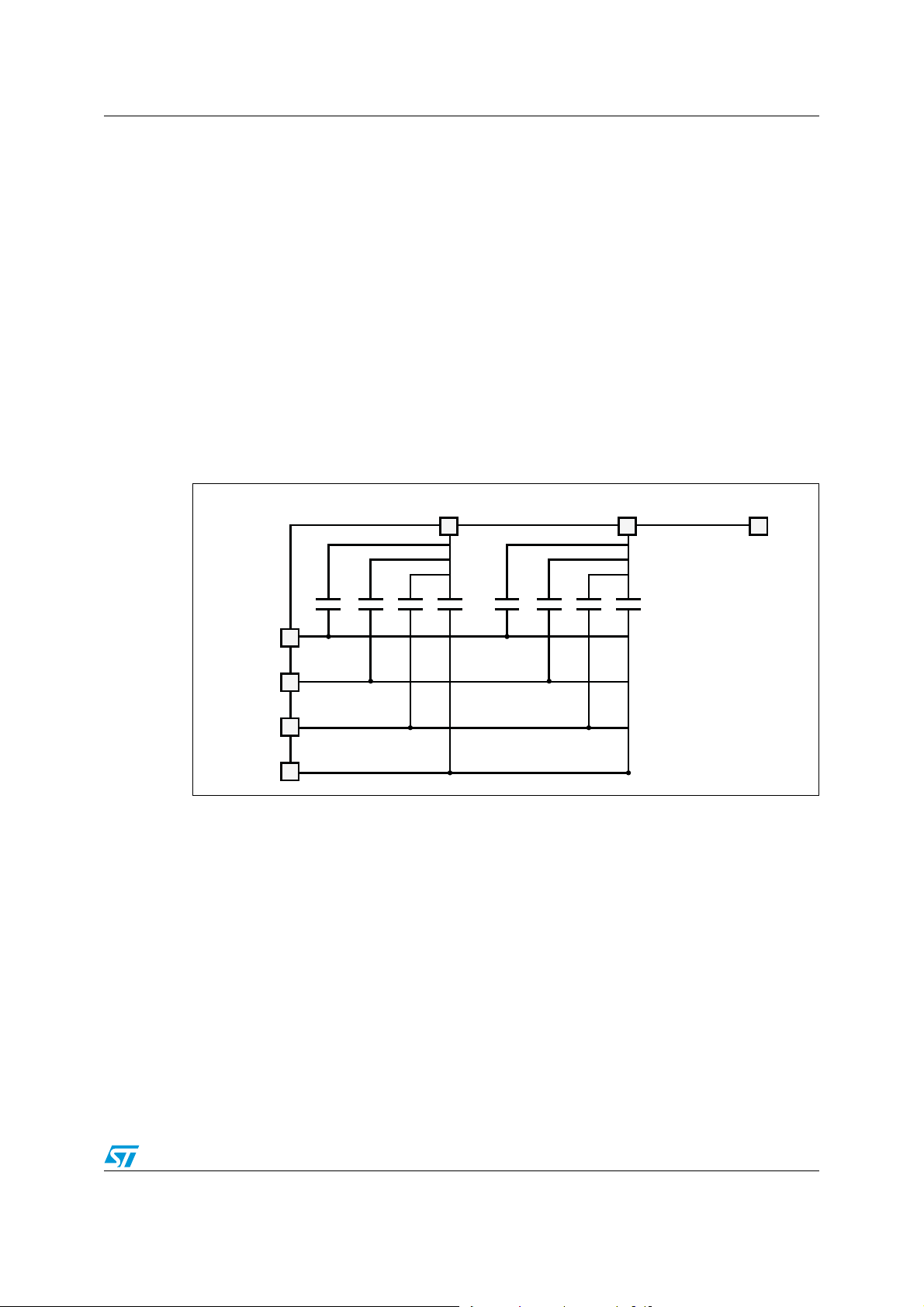
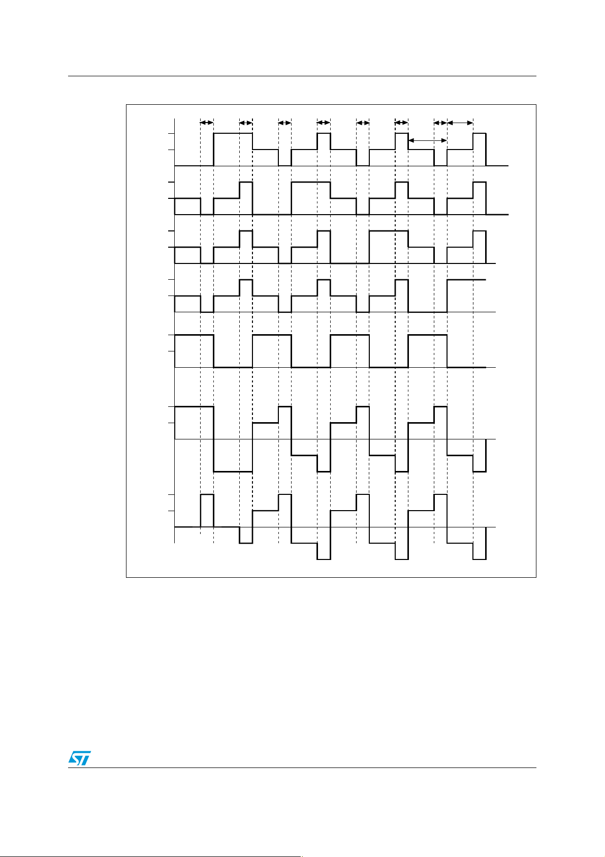
2.3 Quadruplex LCD drive
In a quadruplex LCD drive, four backplanes are used. Each LCD pin is connected to four
LCD segments, whose other side is connected to one of the four backplanes. Thus, only
(S/4)+4 MCU pins are necessary to drive an LCD with S segments. For example, to drive an
LCD with 128 segments (32 ×4), only 36 I/O ports are required (32 I/O ports to drive the
segments, 4 I/O ports to drive the backplanes).
Three different voltage levels have to be generated on the common lines: 0, V
The Segment line voltage levels are 0 and V
only. The LCD segment is inactive if the
DD
/2, VDD.
DD
RMS voltage is below the LCD threshold voltage, and is active if the LCD RMS voltage is
above the threshold. Figure 7 shows typical backplane, Segment and LCD waveforms. The
intermediate voltage V
selected as backplanes are set by firmware to output mode for 0 or V
high-impedance input mode for V
/2 is only required for Backplane voltages. The MCU I/O pins
DD
/2. The VDD/2 voltage is determined by two resistors of
DD
levels and to the
DD
equal value, externally connected to the I/O pins. When one backplane or COM is active, the
other ones are neutralized by applying V
/2 to them.
DD
Figure 6. Basic LCD segment connection in quadruplexed mode
Doc ID 14144 Rev 2 9/33
Page 10
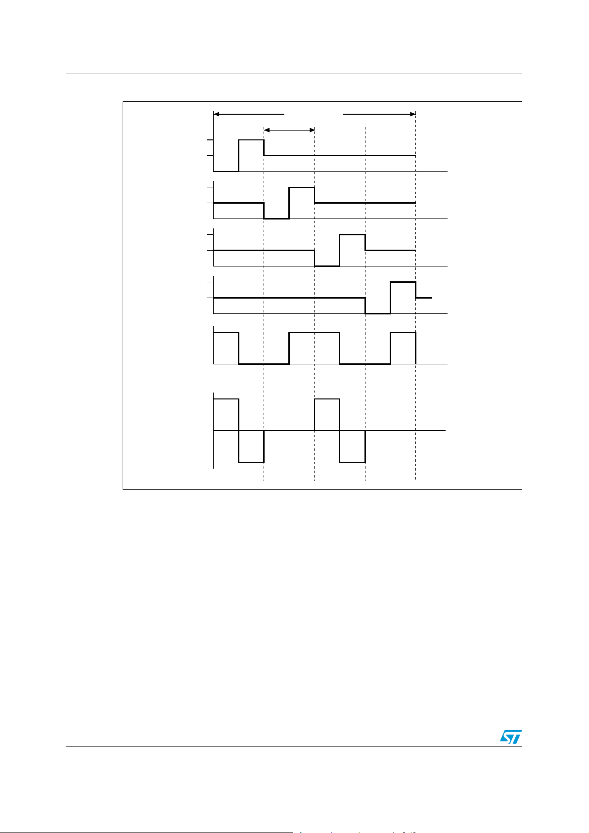
LCD drive signals AN2656
COM1
ai14763
V
COM
+VDD/2
COM2
Segx_1 On Segx_2 Off Segx_3 On Segx_4 Off
Vseg – V
COM
Vseg – V
COM1
Vseg – V
COM4
T/8 T/4 T/2 3T/4 T
COM3
COM4
Vsegx
Control
period
Single-frame period
Figure 7. LCD timing diagram for quadruplex mode
10/33 Doc ID 14144 Rev 2
Page 11
AN2656 LCD drive signals
Segx_1 On
Vsegx
Segx
Vsegx
– V
COM1
Segx_1 Off
ai14765
Vrms ON
1
TxT+
---------------- -
ft2td
0
TXT+
=
Vrms ON
1
TxT+
---------------- -
Vcc2tVcc–2tVcc2
2
tVx
2
t8d
0
xT
8
------ -
+d
2T
8
------ -
T
+d
T
8
---
2T
8
------ -
+d
0
T
8
---
=
Figure 8. LCD timing diagram for a single segment
2.3.1 LCD mean voltage calculation
The LCD mean voltage must be very close to zero to guarantee long life to the LCD. The
LCD mean voltage for On and Off periods can be calculated as shown below:
Vmean(On) = 1/8 Vseg + 1/8 (–V
Vmean(Off) = 3(Vseg/2) + 3(–Vr/2) (2)
Vmean(On) and Vmean(Off) assume identical periods for each phase.
Equating equations (1) & (2) to zero, that is putting Vmean(On) = 0 and Vmean(Off) = 0,
gives: Vseg = V
● V
● Vr/2 is the voltage in the middle of the resistor bridge, applied on the COM line
● Vseg is the maximum voltage on the Segx line
● V
is the maximum voltage on the COM line
COM
is the microcontroller power supply
CC
= Vr = VCC, where:
COM
2.3.2 Contrast calculation
Let the frame period be T + xT, where T is the active time and xT, the dead time. x is the
proportion of dead time and Vx is the voltage during the dead time.
) + 3(Vseg – Vr/2) + 3(–Vr/2) (1)
COM
Doc ID 14144 Rev 2 11/33
Page 12

LCD drive signals AN2656
Vrms ON
1
TxT+
---------------- -
V
CC
2
T
8
---
V
CC
2
T
8
---
V
CC
2
4
-------------
6T
8
------ - Vx
2
xT
8
------ -
8+++
=
Vrms ON
1
1x+
------------
14
V
CC
2
32
------------------------ - Vx2x+
=
Vrms ON
1
1x+
------------
14
V
CC
2
32
-------------------------
=
Vrms ON
1
1x+
------------
0.661V
CC
=
Vrms OFF
1
TxT+
---------------- -
0t0t VCC22tVx
2
t8d
0
xT
8
------ -
+d
2T
8
------ -
T
+d
T
8
---
2T
8
------ -
+d
0
T
8
---
=
Vrms OFF
1
1x+
------------
6
V
CC
2
32
--------------------- - Vx2x+
=
Vrms OFF
1
1x+
------------
0.18V
CC
=
CC
Since Vx = 0 (in case of a decrease in Vrms)
Since Vx = 0 (in case of a decrease in Vrms)
, where Dx = Contrast calculation with contrast
control method
The contrast D, between V
optical contrast by tuning V
and V
ON
close to the threshold value of the LCD.
ON
is constant (quality of contrast). We only change the
OFF
Note: The LCD contrast must be controlled instantaneously by firmware depending on the
external temperature and the supply voltage value. So the user has to measure both the
ambient temperature using a temperature sensor and the microcontroller supply voltage
using for example an ADC channel.
12/33 Doc ID 14144 Rev 2
Page 13

AN2656 Example of a quadruplex LCD with STM32F10xxx
V
DD
470 kΩ
470 kΩ
Resistor
network
Common lines
LCD Glass
Segment lines
PC8-PC11 PD0-PD15
PE0-PE15
16
only for
128-segment LCDs
16
for 64- and 128-segment
LCDs
ai14765
STM32F10xxx
3 Example of a quadruplex LCD with STM32F10xxx
The following example describes a drive for a quadruplex mode (4COM) LCD using the
STM32F10xxx. Refer to Figure 9. The only external components needed for driving the LCD
are eight resistors of 470 k each. To get the best DC voltage on the LCD, the user can use
precision resistors to have a precise V
higher the resistor precision, the lower the DC value.
One I/O port per segment and one I/O port for each COM line are needed to drive the LCD.
For example, to drive a quadruplex LCD that has 128 segments (with 32 segment lines and
4 COM lines) a total of 36 I/O ports only is required.
Figure 9. Hardware connection diagram (1/2 bias control)
/2 when the GPIOs are in high impedance. The
DD
The LCD timing is generated by a timer output-compare interrupt. Each cycle consists of
four phases, one for each backplane. Each COM line generates its waveform during the
corresponding phase, e.g. COM1 line during phase1. During other phases, it remains at
level V
/2. Each phase consists of two parts:
DD
1. Active time
2. Dead time
During the active time, segment lines and common lines are used to drive the LCD. During
the dead time, Segment lines and common lines are used to tune the contrast.
Active time starts after the Output Compare 2 interrupt and dead time starts after the Output
Compare 1 interrupt. A total of 16 interrupts are generated in each frame period with four
Doc ID 14144 Rev 2 13/33
Page 14

Example of a quadruplex LCD with STM32F10xxx AN2656
COM1
ai14766
V
COM
+VDD/2
COM2
Segx_1 Off
T/4 T/2 3T/4 T
COM3
COM4
Vsegx
Control periodDead time Active time
V
COM
+VDD/2
V
COM
+VDD/2
V
COM
+VDD/2
+V
DD
Segx_1 On
V
COM
+VDD/2
cc2_1 cc2_2 cc2_1
cc1 cc1
interrupts per control period. There are 2 Output Compare 2 events (CC2_1 and CC2_2)
and 2 Output Compare 1 events in each phase. These are explained as follows:
● During CC2_1: V
is applied to the segments which have to be turned on and 0 is
DD
applied to the segments which have to be turned off. The Common line which
corresponds to this phase is set to low level. Other Common lines are set to level
V
/2.
DD
● During CC1: to decrease Vrms, all segment lines and Common lines are inactive, that
is set to low level (see Figure 10). To increase Vrms, Common lines are set low and
segment lines are set to high level (see Figure 11).
● During CC2_2: Segment lines are supplied with voltage levels that are inverted
compared to the one applied during CC2_1. The Common line that corresponds to this
phase is set to high level. Other Common lines are set to V
● Again during CC1: to decrease Vrms, all Segments and Common lines are inactive,
DD
/2.
that is set to low level (see Figure 10). To increase Vrms, Common lines are set to high
and Segments lines are set low level (see Figure 11).
Figure 10. LCD timing diagram with active and dead time (to decrease Vrms)
14/33 Doc ID 14144 Rev 2
Page 15
AN2656 Example of a quadruplex LCD with STM32F10xxx
COM1
ai14856
V
COM
+VDD/2
COM2
Segx_1 Off
T/4 T/2 3T/4 T
COM3
COM4
Vsegx
Control period
Dead time Active time
V
COM
+VDD/2
V
COM
+VDD/2
V
COM
+VDD/2
+VDD/2
Segx_1 On
Vsegx
+V
DD
/2
cc2_1 cc2_2
cc1
cc1
Vsegx
Segx On
Figure 11. LCD timing diagram with active and dead time (to increase Vrms)
Doc ID 14144 Rev 2 15/33
Page 16
Example of a quadruplex LCD with STM32F10xxx AN2656
Vsegx
Vcom2
Vsegx-Vcom2
(Mean)
Vcom1
Vcom3
Vcom4
Vcom2
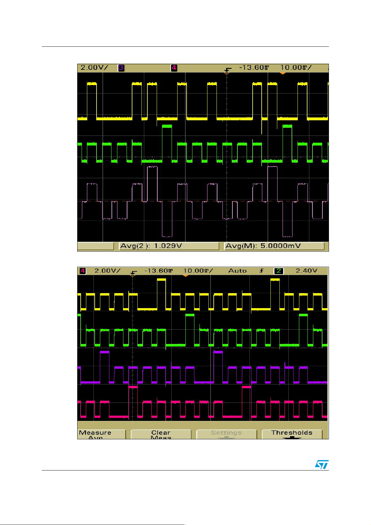
Figure 12. Screenshot of Vcom3 and Vsegx (Segment1 of digit2)
Figure 13. Screenshot of the four common lines
16/33 Doc ID 14144 Rev 2
Page 17
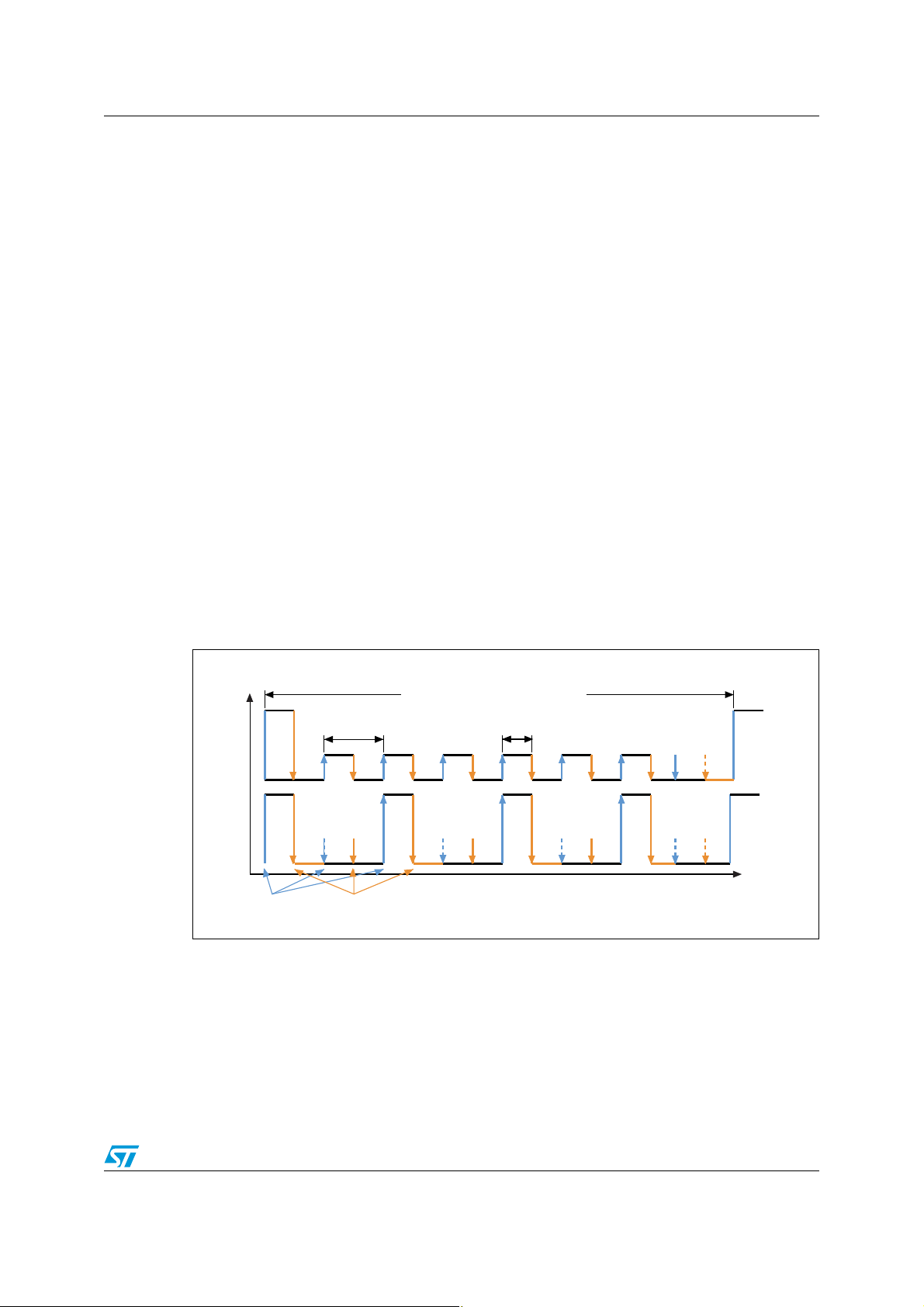
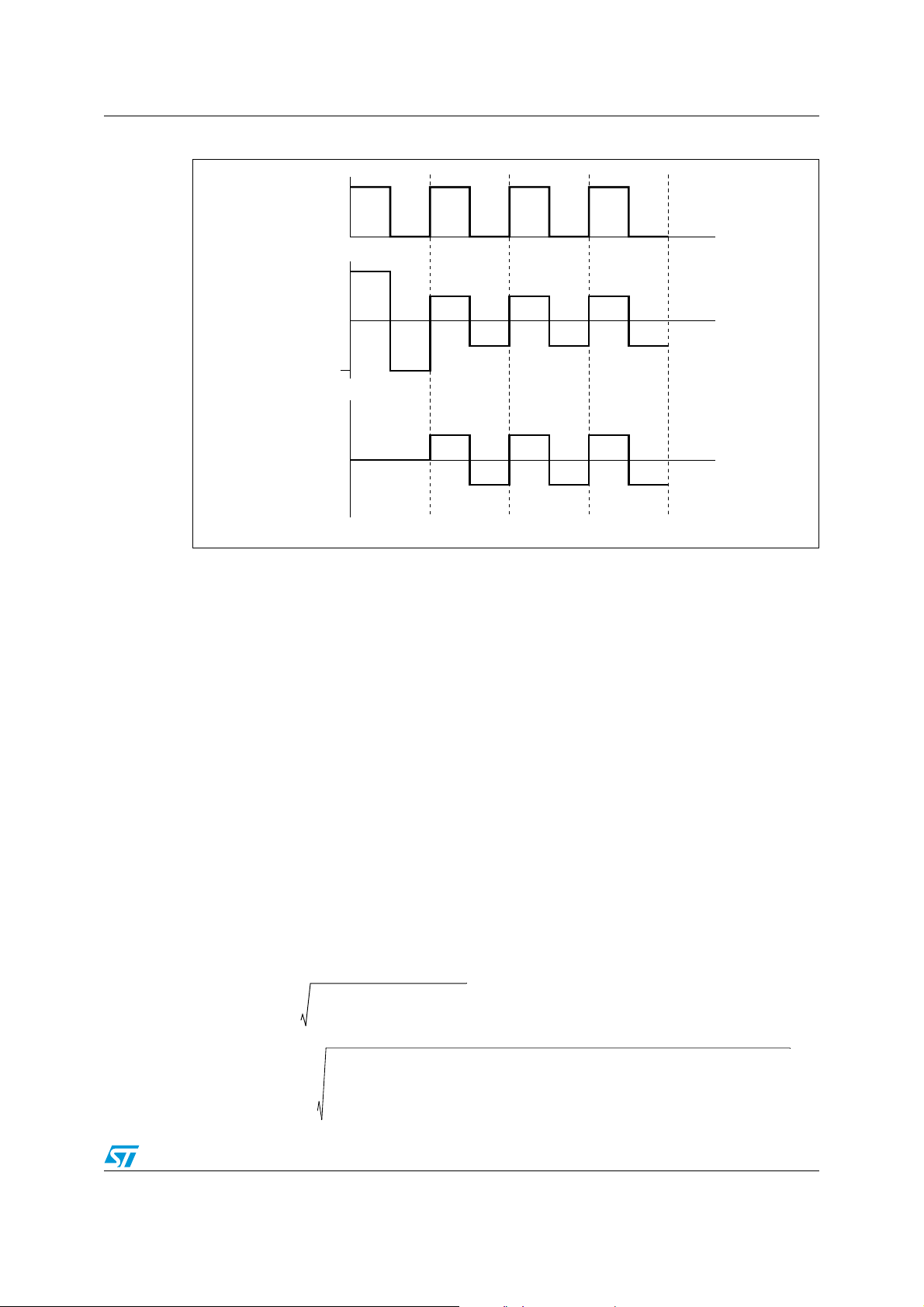
AN2656 Firmware description
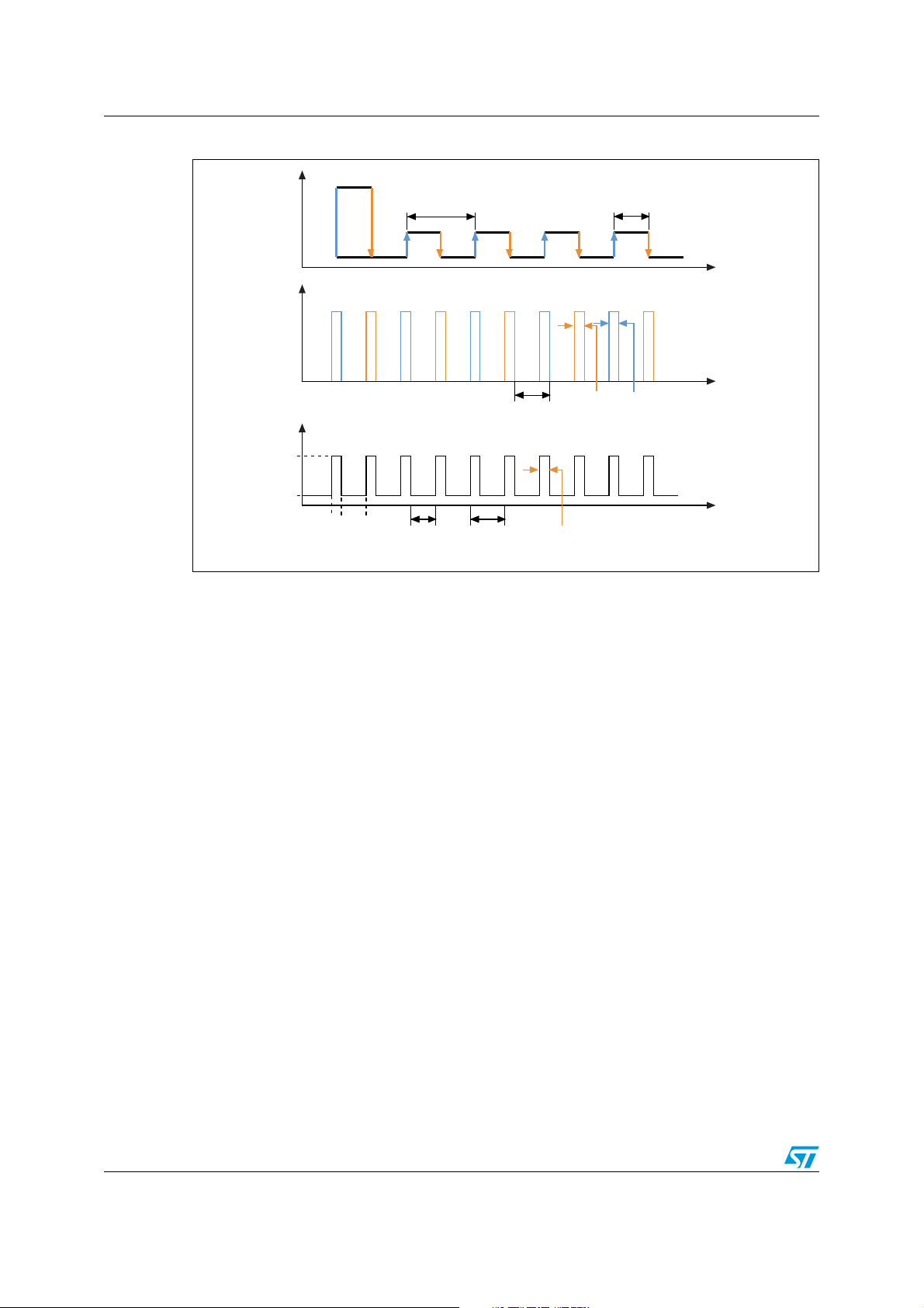
ai14857
V
COMx
Control period = 3.6 ms Active time
Vsegy
U
t
Full period = 3.6 ms × 8 (34.7 Hz)
CC2 CC2
One full cycle, 8 stages/CC2 events = 3.6 × 8 = 28.8 ms (34.7 Hz)
4 Firmware description
In the STM32F10xxx LCD demonstration, the PE0-PE15, PD0-PD15 port pins are
connected to the 32 segment lines and are used to generate the segment signals. The PC8
to PC11 pins are connected to the 4 COM lines and used to generate the COM signals.
The LCD driver consists of five initialization routines (system clock configuration, NVIC
configuration, GPIO initialization, timer configuration and EXTI configuration). To activate
the LCD, these four initialization routines have to be called. After the routines have been
called, the STM32F10xxx gets the timer Output Compare 1 (CC1) and Output Compare 2
(CC2) interrupts.
The ports are flexible, configurable by firmware, that is, the user can change the hardware
implementation with minimum changes in firmware. This is done by changing the defines in
the glasslcd.h file.
Example: the user can change the port to which the common lines are connected (port X),
and its offset, according to PX0 (where X can be A, B C D or E). By default, in the firmware,
common lines COM1 to COM4 are driven by PC8 to PC11, segment lines of lower quarter
digits (Digit1 to Digit4) are connected to port E and segment lines of higher quarter digits
(Digit5 to Digit8) are connected to port D.
The timer used by default in the firmware to drive the LCD is TIM3; it can be changed to
another timer.
Figure 14 presents the LCD timings used in the firmware. The LCD demo consists of
displaying a message on LCD glass.
Figure 14. Timing used by the STM32F10xxx LCD library
In Figure 14, the orange arrows represent CC1 events and the blue arrows represent CC2
events.
The timer interrupt routine is called every 3.6 ms by Output Compare 2 (CC2) to handle LCD
segment switching.
The timer interrupt routine is called again after a delay specified by Output Compare 1
(CC1) to handle contrast control (to switch all voltages off for instance).
Doc ID 14144 Rev 2 17/33
Page 18

Firmware description AN2656
4.1 How to use the LCD library
The firmware is made to be flexible and configurable to adapt to the user’s needs.
4.1.1 How to select the LCD glass by firmware
The implemented firmware can drive two reference types of glass LCD: 64- and 128segment LCDs
● CT4-098: 64 segments (4 digits: 64 segments, manufacturer: ZHIYI Technology)
● PD 878: 128 segments (8 digits: 128 segments, manufacturer: Pacific Display)
● VIM 878: 128 segments (8 digits: 128 segments, manufacturer: Varitronix)
Note: PD 878 and VIM 878 LCDs are pin-to-pin compatible.
These LCDs are selectable by firmware by commenting and uncommenting the following
lines in the glasslcd.h file:
#define USE_LCD_REF_PD_878
#define USE_LCD_REF_CT4_098
To use the first LCD (CT4-098), comment the #define USE_LCD_REF_PD_878 line and
uncomment #define USE_LCD_REF_CT4_098.
To use the second LCD (PD 878 or VIM 878), comment the #define
USE_LCD_REF_CT4_098 line and uncomment #define USE_LCD_REF_PD_878.
For each case, the letter and number map has to be initially selected in the preprocessor.
Note: The user has to comment one of the line and uncomment the other (select one type of LCD
reference), otherwise the compiler generates an error.
4.1.2 How to select GPIOs to connect the LCD glass to STM32F10xxx
Each digit (16 segments) is driven by 4 common lines and 4 segment lines to form a matrix
of 16 segments. So each digit occupies 4 GPIOs to drive the common lines and 4 others to
drive the segment Lines. (common lines and segment lines are driven by different ports).
18/33 Doc ID 14144 Rev 2
Page 19

AN2656 Firmware description
The first digit
(16 segments)
Digit1.........................Digit4
Digit1...................Digit4 Digit5....................Digit8
Lower quarter digits
(lower 4 digits)
Higher quarter digits
(higher 4 digits)
Lower quarter digits alone
ai14858
Figure 15. LCD timing diagram for a single segment
Segment line configuration
(Refer toTa bl e 3 for more pinout details.)
CT4-098 has 16 segment lines and 4 common lines, so one port (16 GPIOs) is reserved for
the segment lines and the common lines are connected to another GPIO port (refer to CT4098 LCD Glass datasheet).
If PD-878 is selected, two ports are reserved for segment lines and the 4 common lines are
connected to a third one (refer to PD-878 LCD Glass datasheet).
The configuration of segment lines is made by modifying the following lines:
#define SegmentsLines_LQD_Port GPIOE
#define SegmentsLines_HQD_Port GPIOD
The first line is used to select the port connected to the LCD segment lines of the first 4
digits (LQD: lower quarter digits), the second line is used to select the second 4 digits (HQD:
higher quarter digits). Refer to Figure 9.
In the configuration shown above port E drives digit 1 to digit 4 and port D drives digit 5 to
digit 8.
Note: In the case where CT4-098 LCD Glass is selected, the second line has no effect.
Common line configuration:
The two LCDs have 4 common lines (COM1 to COM4). The firmware configuration is done
in the glasslcd.h file using the three following lines:
#define CommonLines_Port GPIOC
//#define CommonLines_EightHighPortPins
#define CommonLines_Pin_Offset 0
Doc ID 14144 Rev 2 19/33
Page 20
Firmware description AN2656
The first line defines the port to which common lines are connected (in the case shown
above, the common lines are connected to port C, they cannot be connected to the same
port as the segment lines).
The second line is used to determine to which eight port pins the common lines are
connected.
● Lower eight port pins: PX0 to PX7
● Higher eight port pins: PX8 to PX15
So if #define CommonLines_EightHighPortPins is commented, COM1 to COM4
are connected to GPIOs with a range of 0 to 7. Otherwise (the line is uncommented), the
common lines are connected to GPIOs with a range of 8 to 15.
The third line defines the offset pin regarding pin0 or pin8 (depending on whether the
second line is commented or not). CommonLines_Pin_Offset value must not exceed 4
(0 to 4), otherwise the firmware does not work correctly.
In the configuration shown above, COM1 is connected to PC8, COM2 to PC9, COM3 to
PC10 and COM4 to PC11.
If #define CommonLines_EightHighPortPins is uncommented, COM1 is connected
to PC8, COM2 to PC9, COM3 to PC10 and COM4 to PC11.
The user has to configure the used GPIO APB clocks in the line below:
#define RCC_APB1Periph_Used_GPIO RCC_APB2Periph_GPIOC \
| RCC_APB2Periph_GPIOD \
| RCC_APB2Periph_GPIOE
Timer selection
Three lines have to be configured by the user:
#define TIMER_LCD TIM3
#define TIMx_IRQChannel TIM3_IRQChannel
#define RCC_APB1Periph_TIMx RCC_APB1Periph_TIM3
The first line, determines which timer will drive the LCD. The second line determines which
IRQ channel will be used to generate the interrupt. The third line configures the APB timer
clock.
In the configurations shown above, TIM3 drives the LCD.
If the user wants to change the default timer, the 3 above mentioned lines have to be
changed. Also, and all the code in the TIM3_IRQHandler() function has to be cut/pasted to
the used timer IRQ handler. For example, if TIM2 is used, the code in TIM3_IRQHandler()
must be moved into TIM2_IRQHandler().
4.1.3 How to select the timer interrupt priority that drives the LCD
Refer to Section 4.2 for more details.
20/33 Doc ID 14144 Rev 2
Page 21

AN2656 Firmware description
4.1.4 LCD contrast control
The firmware contrast control is under pending patent from STMicroelectronics. The use of
this technique with a non-STMicroelectronics microcontroller has to be agreed by
STMicroelectronics.
LCD contrast is entirely controlled by firmware without the use of any external components.
LCD contrast can be adjusted to the optimal value depending on the operating voltage of the
LCD used. It is controlled by varying the dead phase timing as shown in the LCD timing
diagram(Figure 7 and Figure 8).
Dead time can be used to decrease or increase the rms voltage (Vrms) of the LCD. Dead
time is the voltage compensation time to regulate the rms voltage up and down. Dead time
can be implemented either after each control period or at the end of the frame. To avoid
flickering, the dead time must be adjusted depending on the LCD quality and the frame
frequency.
In the example shown in Figure 10, the rms value of the LCD decreases when the dead time
increases and rms value increases when the dead time decreases. In Figure 11, it works in
the opposite way.
The LCD_SettingContrast() function controls the LCD contrast that sets the channel2
pulse length.
Example
uint16_t ContrastValue = 0xE5C;
LCD_SettingContrast(ContrastValue);
ContrastValue has a range of 0x0000 to 0x1CB8.
The 0x0000 value corresponds to the maximum contrast: the LCD is completely dark (100%
duty cycle).
The 0x1CB8 value corresponds to the minimum contrast: the LCD is completely transparent
(0% duty cycle).
4.2 LCD timer interrupt
The LCD interrupt routine (or TIMER_LCD: the timer used to drive the LCD glass) is
optimized to have the minimum DC voltage value. Direct access to registers is used to
reduce the execution time and the jumping time arising from function calls.
4.2.1 LCD with high interrupt priority
In this configuration, the LCD always has the high interrupt priority (priority 0). It interrupts all
other ongoing interrupts and no interrupt can interrupt an LCD interrupt.
To run the LCD in this configuration:
● Modify the value of the interrupt priority in the glasslcd.h file as follows:
#define LCD_Priority_Value 0 /* LCD priority value = 0 */
● Comment this line in the glasslcd.h file as follows:
// #define LCD_Use_Boost_Priority
Doc ID 14144 Rev 2 21/33
Page 22

Firmware description AN2656
Impact
In this case the Vseg and Vcom pulses are kept at the same width, so the DC voltage value
is kept near 0 V (in the worst case 5 mV).
The PD-878 manufacturer specifies that the maximum allowed DC voltage is 50 mV. So
here we have a DC voltage 10 times less than the value specified by the manufacturer.
4.2.2 LCD with low-high interrupt priority (using boosting priority)
When the LCD is configured in low-high interrupt priority, the LCD interrupt priority toggles
between a low priority value and the highest priority value.
By default, the LCD interrupt is configured with the lowest priority value (configuration in
main()). When the interrupt occurs, the LCD priority interrupt is boosted to have the highest
priority (priority 0), so that no other interrupt can interrupt it. Before returning from the LCD
interrupt, its priority returns to the previous lowest priority value defined by the user in the
glasslcd.h file. This avoids a delay between the setting of the GPIO segment line and
common line pins subsequent to decreasing the DC voltage value.
This boosting is performed using the priority boosting mechanism of the Cortex-M3 core on
which the STM32F10xxx microcontroller is based.
To run the LCD in this configuration:
● Modify the value of the interrupt priority in the glasslcd.h file to the lowest priority value:
#define LCD_Priority_Value 6 /* LCD priority value = 6 */
The lowest user interrupt priority value in this case is 5. So the LCD interrupt priority
value must be lower than the lowest user interrupt priority.
● Ucomment this line in the glasslcd.h file as follows:
#define LCD_Use_Boost_Priority
Impact
The user firmware is never interrupted by the LCD interrupt.
The DC voltage is higher than the DC value presented in the previous configuration (LCD in
higher priority). This is due to user interrupts that have the highest priority and occur at the
same time as the LCD interrupt (with lowest priority). So the LCD interrupt is a nested
interrupt and is delayed until the user interrupt execution is finished. This causes an
inequality between segment and com pulses (Vseg and Vcom pluses are not kept at the
same width), consequently the DC voltage is increased in accordance with the number of
user interrupts and their execution time.
So the higher the number of user interrupts that postpone the LCD execution, the higher the
DC voltage. The higher the execution time of the user interrupt that postpones the LCD
execution, the higher the DC voltage.
In this configuration, the measured DC value is 18 mV (depending on the number of user
interrupts that postpone the LCD interrupt, and their execution time).
The PD-878 manufacturer specifies that the maximum allowed DC voltage is 50 mV. Here,
we have a DC voltage 2.5 times less than the value specified by the manufacturer.
22/33 Doc ID 14144 Rev 2
Page 23

AN2656 Firmware description
4.2.3 LCD interrupt always with lowest priority
The LCD interrupt always has the lowest priority. All user interrupts can interrupt the LCD
execution, and the LCD interrupt cannot interrupt any other interrupt.
To run the LCD in this configuration:
● Modify the value of the interrupt priority in the glasslcd.h file to the lowest priority:
#define LCD_Priority_Value 6 /* LCD priority value = 6 */
The lowest user interrupt priority value in this case is 5. So the LCD interrupt priority
value must be lower than the lowest user interrupt priority.
● Comment this line in glasslcd.h file as follows:
// #define LCD_Use_Boost_Priority
Impact
The DC voltage is higher than the DC value presented in the two previous configurations
(LCD with higher priority and boosted LCD priority).
This is due to:
● The user interrupts that interrupt the LCD routine between the settings of segment line
and common line GPIOs. An undesirable jitter appears on the Vseg-Vcom signals, and
its average is added to the DC value of Vseg-Vcom, consequently the DC value is
increased.
● The user interrupts that have highest priority and occur at the same time as the LCD
interrupt (with lowest priority). The LCD interrupt is a nested interrupt and is delayed
until user interrupt execution is finished. This causes the inequality of the segment line
and common line pulses, consequently the DC voltage is increased according to the
number of user interrupts and their execution time.
In this configuration, we can measure a DC value of about 50 mV (depending on the number
of user interrupts that delay or interrupt the LCD interrupt and their execution time).
4.3 Default demo configurations
● The firmware runs from a CPU with a 2 MHz frequency.
● The used LCD is PD-878 (or VIM 878)
● Segment lines of the lower quarter digits are connected to port E
● Segment lines of the higher quarter digits are connected to port D
● Common lines are connected to port C
● The four common lines are connected as follows: COM1 to PC8, COM2 to PC9, COM3
to PC10 and COM4 to PC11
● TIM3 drives the LCD glass
● LCD priority value = 3
● Boost priority is used (at entry LCD interrupt the priority = 0, at exit the interrupt routine
priority returns to 3)
When the user runs the demonstration, the “STM32” message is displayed on the LCD
glass.
Doc ID 14144 Rev 2 23/33
Page 24

LCD glass in battery-powered and low-power applications AN2656
470 kΩ
470 kΩ
Resistor
network
Common lines
LCD Glass
Segment lines
PC8-PC11 PD0-PD15
PE0-PE15
16
only for
128-segment LCDs
16
for 64- and 128-segment
LCDs
ai15408
STM32F10xxx
PC7
LCD_BIAS+
5 LCD glass in battery-powered and low-power
applications
This section describes how to manage the LCD glass in low-power designs like batterypowered applications. It is divided into two parts. The first part describes, the timer method
for driving the LCD glass using the STM32F10xxx Sleep mode. The second part describes
how to drive the LCD glass using the RTC feature combined with the STM32F10xxx Stop
mode to have minimum power consumption.
5.1 Hardware implementation
The hardware is the same as the one described in Section 3, except for an additional line
called LCD_Bias+, that is added to power off the LCD, and so save power, when the
application enters a low-power mode. All segments and all common lines are set to 0 V, thus
preventing any Leakage current on the GPIOs.
Figure 16. Hardware connection diagram (1/2 bias control)
LCD bias pin configuration by software
24/33 Doc ID 14144 Rev 2
#define LCD_Bias_Port GPIOC
#define LCD_BiasPlus_Pin GPIO_Pin_7
The first line defines the port to which the LCD_BIAS+ pin is connected to power on/off the
LCD glass. The second line defines the GPIO pin to be connected to LCD_BIAS+.
Page 25

AN2656 LCD glass in battery-powered and low-power applications
CC1
Task
TIM CC1
interrupt
CC2_1
Task
TIM CC2
interrupt
CC2_2
Task
TIM CC2
interrupt
Sleep
CC2 interrupt occured
Return from interrupt
CC2_1_Phase_Execute = 0
CC2 interrupt occured
CC2_1_Phase_Execute = 1
Return from interrupt
CC1 interrupt occurred
Return from interrupt
ai14858
5.2 LCD glass managed by the timer using the Sleep low-power mode
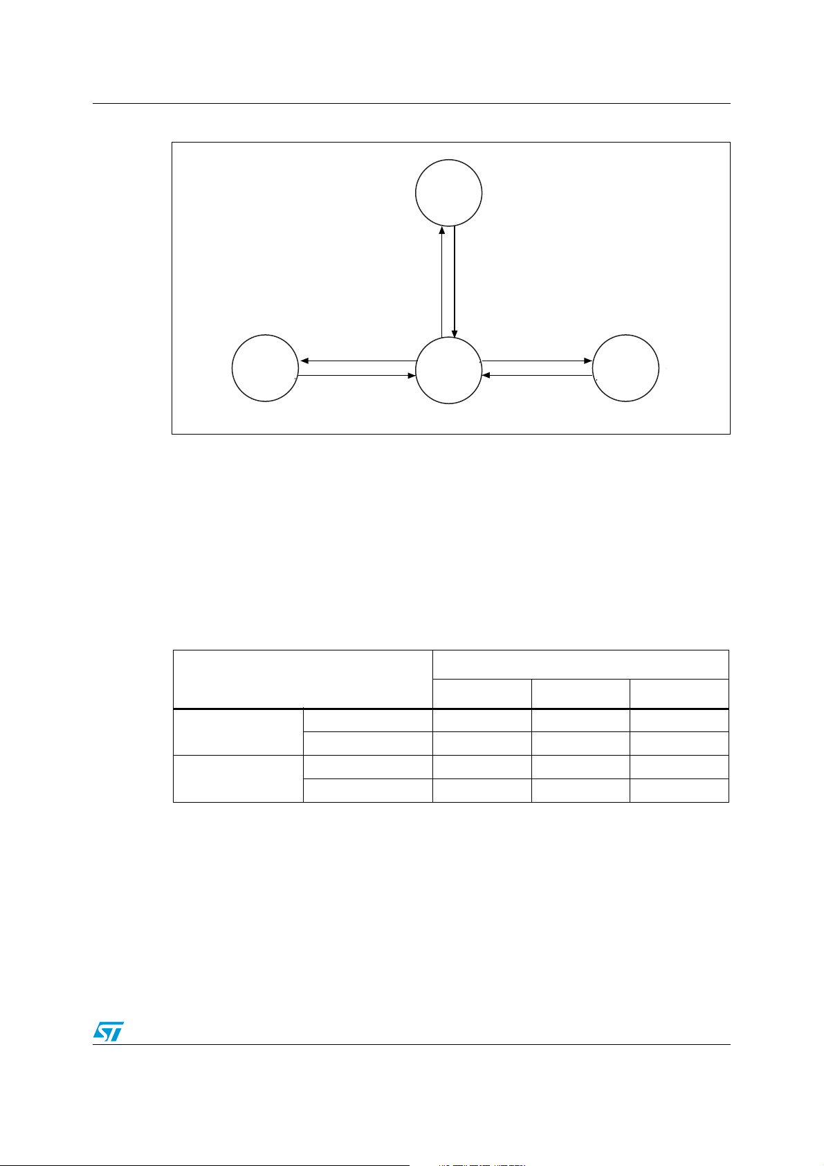
As described previously, the timer method is based on the output compare interrupt (CC1
and CC2). CC2 is divided into two tasks called CC2_1 and CC2_2, which are managed
(enabled) by a software flag (CC2_1_Phase_Execute). Figure 17 shows the timer method
state machine that explains the interactions of the different tasks.
Figure 17. Timer method state machine
5.2.1 Some current and CPU load measurements
Some current measurements are provided in Ta bl e 1 . These measurements correspond to
the (microcontroller + resistor network + LCD glass) consumption.
The measurement conditions are:
● Hardware environment: STM32F103xx is used, LCD ref: PD-878, HSI (internal RC)
clock is used, power supply = 3 V, HCLK = PCLK1 = PCLK2
● Tool chain: IAR 4.42, configuration: high optimization on size, Inline threshold = 16.
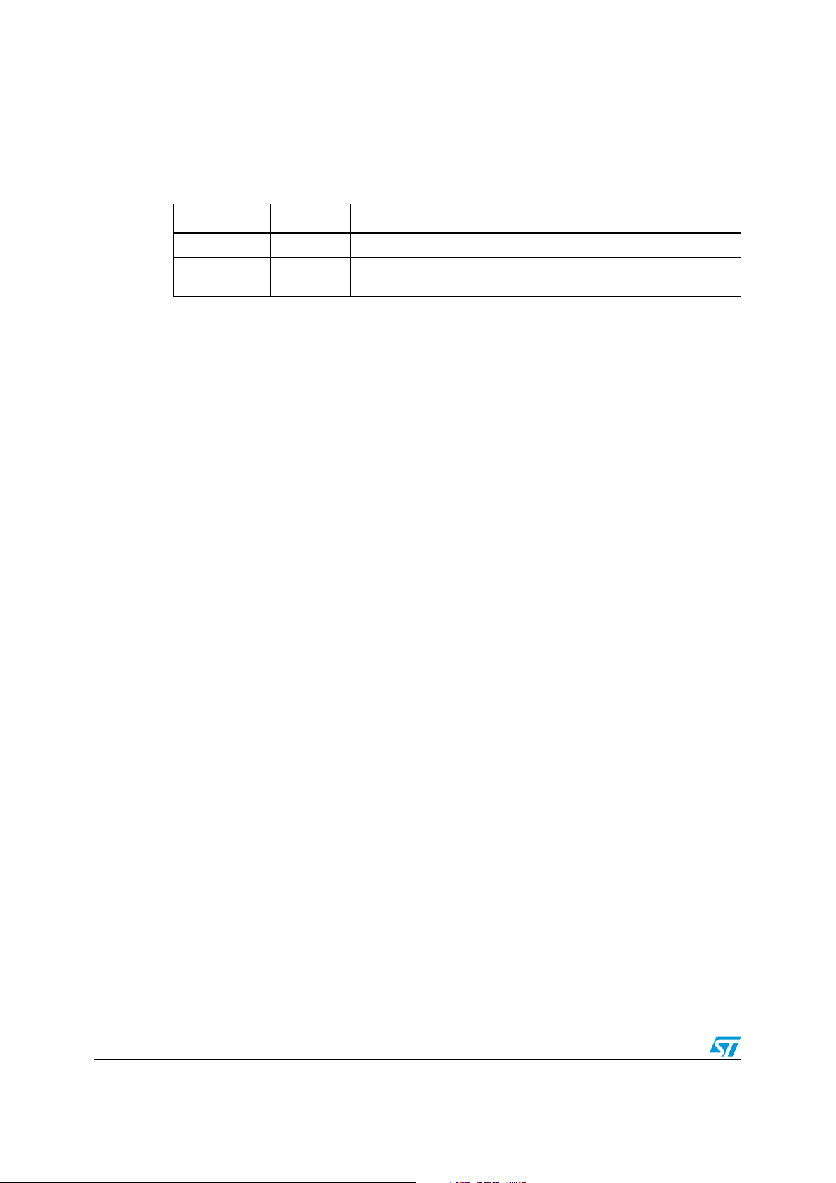
Table 1. Current consumption vs. frequency
CPU load/
Consumption
Execution from Flash
Execution from RAM
CPU load 4.68% 2.33% 1.18%
Consumption 629 µA 742 µA 882 µA
CPU load 5.91% 3.39% 1.57%
Consumption 584 µA 676 µA 866 µA
HCLK frequency
1 MHz 2 MHz 4 MHz
Doc ID 14144 Rev 2 25/33
Page 26
LCD glass in battery-powered and low-power applications AN2656
ai14860
Control period = 3.6 ms Active time = 3.6/2 = 1.8 ms
U
t
CC2_2 CC1
t
Timer Interrupts
(Run mode)
Sleep mode
CC2_1 CC1 CC2_2
I (µA)
t
I
RUN
I
WFI
0
T1 T
Sleep modeT2Period T Run mode
T1
TT1T2+=
Im
1
T
---
it td
0
T
1
T
---
I
RUN
td
0
T1
1
T
---
I
Sleep
td
T1
T
+
T1
T
------ -
I
RUN
TT1–
T
---------------- -
I
Sleep
+
T1
T
------ -
I
Run
T2
T
------ -
I
Sleep
+== = =
Figure 18. Timer method chronogram (in this case duty cycle = 50%)
Period T is the sum of the interrupt execution time and the Sleep time:
Mean current Im can be calculated as shown below:
5.3 LCD glass managed by the RTC and using the Stop lowpower mode
The RTC method is based on RTC Alarm interrupt and software flags. There are three tasks
Task1, Task2 and Task3 instead of CC1, CC2_1 and CC2_2, respectively, in the timer
method.
The RTC alarm register is updated each time Task1, Task2 or Task3 is executed, to have the
timings needed to drive the LCD glass.
The RTC Alarm interrupt has the capability to wake up the core from the Stop mode (EXTI
line 17).
Figure 19 shows how the RTC method works and how the tasks are organized to generate
the adequate signals to drive the LCD glass using the Stop mode to minimize power
consumption. The sequence of the three tasks is managed by two software flags:
EnableTask1 and EnableTask2_3.
The contrast is defined in the glasslcd_RTC.h file and can be modified by the user (the value
is in percent):
#define LCDContrastValue 50 /* Set LCD contrast to 50% */
26/33 Doc ID 14144 Rev 2
Page 27
AN2656 LCD glass in battery-powered and low-power applications
Task1
RTC Alarm
interrupt
STOP
Task2
RTC Alarm
interrupt
Task3
RTC Alarm
interrupt
-EnableTask1 = FALSE
-RTC Alarm occured
-Return from interrupt
-Return from interrupt
-EnableTask2_3 = TRUE
-EnableTask1 = FALSE
-RTC Alarm occured
-EnableTask2_3 = FALSE
- RTC Alarm occurred
- EnableTask1 = TRUE
- Return from interrupt
ai14861
Figure 19. RTC method state machine
5.3.1 Some current and CPU load measurements
Some current measurements are presented in Tab l e 2. They correspond to the
(microcontroller + resistor network + LCD glass) consumption.
The measurement conditions are:
● Hardware environment: STM32F103xx is used, LCD ref: PD-878, HSI (high-speed
internal RC) clock is used, LSI (low-speed internal) clock is used, power supply = 3 V,
HCLK = PCLK1 = PCLK2
● Tool chain: IAR 4.42, configuration: high optimization on size, Inline threshold = 16.
Table 2. Current consumption vs frequency
HCLK frequency
CPU load/consumption
1 MHz 2 MHz 4 MHz
Flash Execution
RAM Execution
CPU load 17.55% 13.42% 10.52%
Consumption 280 µA 258 µA 290 µA
CPU load 20.31% 15.02% 10.63%
Consumption 193 µA 174 µA 178 µA
Doc ID 14144 Rev 2 27/33
Page 28

LCD glass in battery-powered and low-power applications AN2656
ai14862
Control period = 3.6 ms Active time = 3.6/2 = 1.8 ms
U
t
Task3 Task1
t
RTC Interrupts
(Run mode)
T1
Stop mode
T2
Task2 Task1 Task3
I (µA)
t
I
RUN
I
STOP
0
T1 T
Stop modeT2Period T Run mode
T1
Period T
TT1T2+=
Im
1
T
---
it td
0
T
T1
T
------ -
I
Run
T2
T
------ -
I
STOP
+==
Figure 20. RTC method chronogram
Period T is the sum of the interrupt execution time and the Stop time:
Mean current Im is expressed by the following equation
28/33 Doc ID 14144 Rev 2
Page 29

AN2656 Comparison of the timer and RTC methods
6 Comparison of the timer and RTC methods
6.1 Timer method
● One timer is used (two Output Compare): the two remaining Output Compare are free
and can be used for another application.
● Very low CPU load: 4.6% at 1 MHz
However:
● The timer configuration depends on the APB1 clock configuration
● In low-power mode, the only supported mode is Sleep mode
6.2 RTC method
● Stop mode supported: minimum power consumption at 2 MHz ~ 174 µA typical
● RTC configuration independent of the APB clock configuration.
However:
● RTC is not available for the calendar feature.
● More instructions are required to execute in RTC Alarm interrupt (enter the
configuration mode, poll on the RTOFF flag, etc.): higher CPU load.
● Some peripherals do not support the Stop mode to wake up the core: additional
software is required to manage this feature.
Doc ID 14144 Rev 2 29/33
Page 30
Hardware implementation AN2656
Digit 1..............................................Digit8
, , , ,
17
18
19
20
21
22
23
24
25
26
27
28
29
30
31
32
33
34
35
36
, , , ,
1
2
3
4
5
6
7
8
9
10
11
12
13
14
15
16
LCD-8 Digits
PD-878 or VIM 878
R7
470k
R8
470k
R1
470k
R2
470k
R5
470k
R6
470k
R3
470k
R4
470k
C2
10uF
C3
100nF
C4
100nF
C5
100nF
C6
100nF
C7
100nF
C8
1uF
C9
10nF
BOOT0
94
NC
73
NRST
14
OSC_IN
12
OSC_OUT
13
PA0-WKUP23PA124PA225PA326PA429PA530PA631PA732PA867PA968PA1069PA1170PA1271PA13/JTMS/SWDIO72PA14/JTCK/SWCLK
76
PA15/JTDI77PB035PB136PB2/BOOT137PB3/JTDO89PB4/JNTRST90PB591PB692PB793PB895PB996PB1047PB1148PB1251PB1352PB1453PB15
54
PC015PC116PC217PC318PC433PC534PC663PC764PC865PC9
66
PC1078PC1179PC12
80
PC13-TAMPER-RTC
7
PC14-OSC32_IN
8
PC15-OSC32_OUT
9
PD081PD182PD283PD384PD485PD586PD687PD788PD855PD9
56
PD1057PD1158PD1259PD1360PD1461PD15
62
PE097PE198PE21PE32PE43PE54PE65PE738PE839PE9
40
PE1041PE1142PE1243PE1344PE1445PE15
46
VDD_150VDD_275VDD_3
100
VDD_428VDD_511VDDA
22
VREF-20VREF+
21
VSS_149VSS_274VSS_399VSS_427VSS_5
10
VSSA
19
VBAT
6
U1STM32F103VBT6
VDD
S1
SW-PB
RESET
C1
100nF_X7R_0603
R9
10K_1%_0603
VDD
L1
Ferrite Bead
VDDA
VDDA
COM1 COM2 COM3 COM4
LCDBIAS+
LCDBIAS+
COM1
COM2
COM3
COM4
COM1
COM2
COM3
COM4
S3-D1
S3-D1
S2-D1
S3-D2
S2-D2
S3-D3
S2-D3
S3-D4
S2-D4
S3-D5
S2-D5
S3-D6
S2-D6
S3-D7
S2-D7
S3-D8
S2-D8
S1-D8
S0-D8
S1-D7
S0-D7
S1-D6
S0-D6
S1-D5
S0-D5
S1-D4
S0-D4
S1-D3
S0-D3
S1-D2
S0-D2
S1-D1
S0-D1
S2-D1
S1-D1
S0-D1
S3-D2
S2-D2
S1-D2
S0-D2
S3-D3
S2-D3
S1-D3
S0-D3
S3-D4
S2-D4
S1-D4
S0-D4
S3-D5
S2-D5
S1-D5
S0-D5
S3-D6
S2-D6
S1-D6
S0-D6
S3-D7
S2-D7
S1-D7
S0-D7
S3-D8
S2-D8
S1-D8
S0-D8
SWO
SWCLK
SWDIO
R10
10K_1%_0603
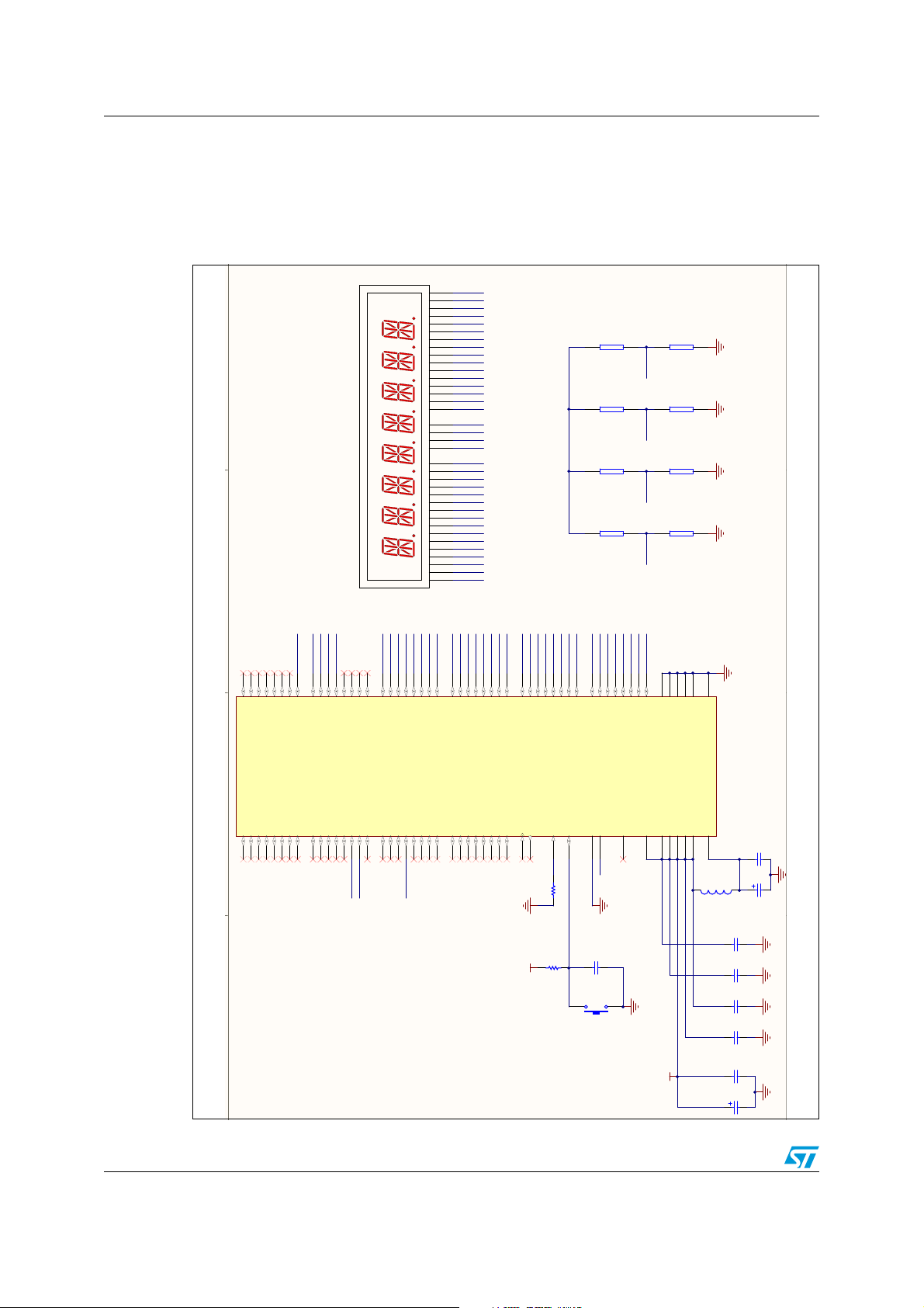
7 Hardware implementation
7.1 Schematic
Figure 21. LCD - STM32F10xxx connection example
30/33 Doc ID 14144 Rev 2
Page 31
AN2656 Hardware implementation
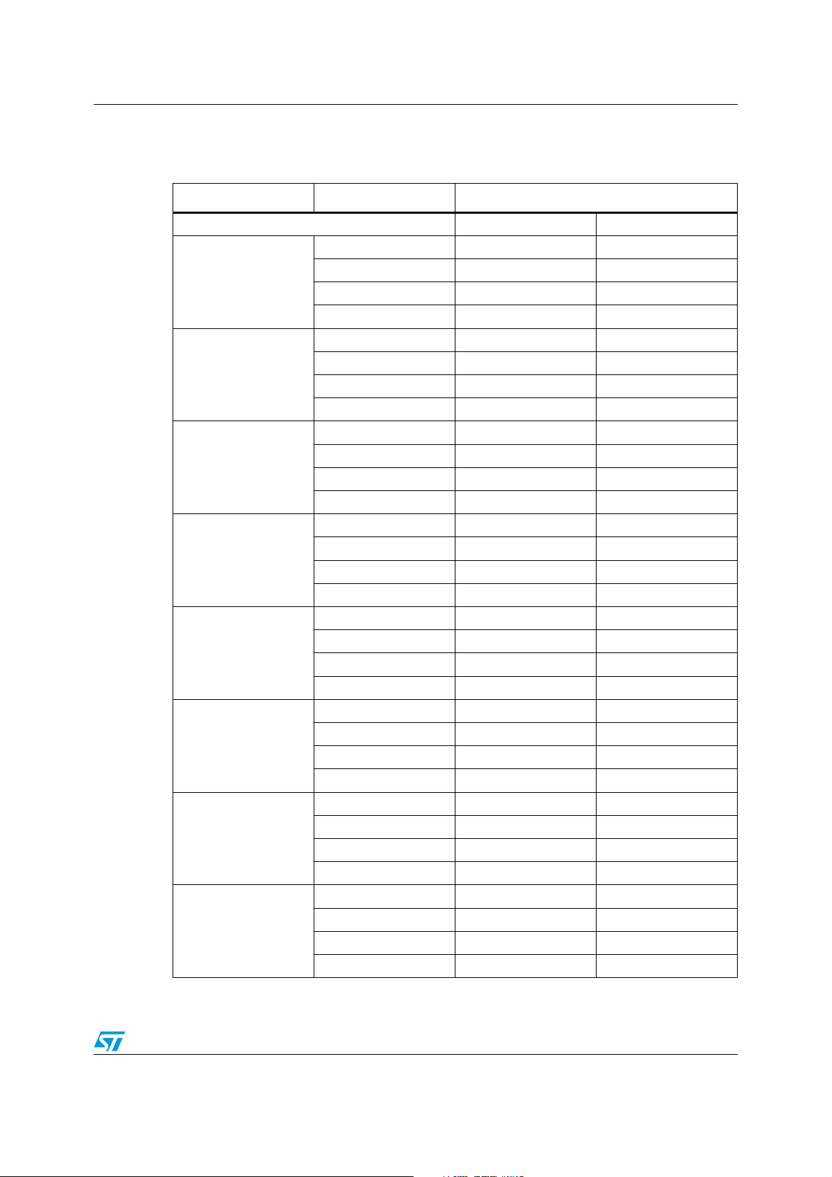
7.2 LCD segment line connections
Table 3. LCD segment line mapping
Digit Segment line
LCD reference -> CT4-098 PD-878
S0 (PX.0) 1 1
S1 (PX.1) 2 2
1
S2 (PX.2) 3 35
S3 (PX.3) 4 36
S0 (PX.4) 5 3
S1 (PX.5) 6 4
2
S2 (PX.6) 7 33
S3 (PX.7) 8 34
S0 (PX.8) 9 5
S1 (PX.9) 10 6
3
S2 (PX.10) 11 31
S3 (PX.11) 12 32
S0 (PX.12) 13 7
S1 (PX.13) 14 8
4
S2 (PX.14) 15 29
S3 (PX.15) 16 30
S0 (PY.0) - 9
S1 (PY.1) - 10
5
S2 (PY.2) - 27
S3 (PY.3) - 28
S0 (PY.4) - 11
S1 (PY.5) - 12
6
S2 (PY.6) - 25
S3 (PY.7) - 26
S0 (PY.8) - 13
S1 (PY.9) - 14
7
S2 (PY.10) - 23
S3 (PY.11) - 24
S0 (PY.12) - 15
8
S1 (PY.13) - 16
S2 (PY.14) - 21
S3 (PY.15) - 22
(1)
LCD pin number
1. X and Y represent the ports to which the segment lines are connected, X is different from Y, and X,Y can
be: A,B,C,D or E.
Doc ID 14144 Rev 2 31/33
Page 32
Revision history AN2656
8 Revision history
Table 4. Document revision history
Date Revision Changes
22-Jul-2008 1 Initial release.
30-Apr-2009 2
Example modified in Section 4.1.4: LCD contrast control.
Titles of Figure 18 and Figure 19 modified.
32/33 Doc ID 14144 Rev 2
Page 33

AN2656
Please Read Carefully:
Information in this document is provided solely in connection with ST products. STMicroelectronics NV and its subsidiaries (“ST”) reserve the
right to make changes, corrections, modifications or improvements, to this document, and the products and services described herein at any
time, without notice.
All ST products are sold pursuant to ST’s terms and conditions of sale.
Purchasers are solely responsible for the choice, selection and use of the ST products and services described herein, and ST assumes no
liability whatsoever relating to the choice, selection or use of the ST products and services described herein.
No license, express or implied, by estoppel or otherwise, to any intellectual property rights is granted under this document. If any part of this
document refers to any third party products or services it shall not be deemed a license grant by ST for the use of such third party products
or services, or any intellectual property contained therein or considered as a warranty covering the use in any manner whatsoever of such
third party products or services or any intellectual property contained therein.
UNLESS OTHERWISE SET FORTH IN ST’S TERMS AND CONDITIONS OF SALE ST DISCLAIMS ANY EXPRESS OR IMPLIED
WARRANTY WITH RESPECT TO THE USE AND/OR SALE OF ST PRODUCTS INCLUDING WITHOUT LIMITATION IMPLIED
WARRANTIES OF MERCHANTABILITY, FITNESS FOR A PARTICULAR PURPOSE (AND THEIR EQUIVALENTS UNDER THE LAWS
OF ANY JURISDICTION), OR INFRINGEMENT OF ANY PATENT, COPYRIGHT OR OTHER INTELLECTUAL PROPERTY RIGHT.
UNLESS EXPRESSLY APPROVED IN WRITING BY AN AUTHORIZED ST REPRESENTATIVE, ST PRODUCTS ARE NOT
RECOMMENDED, AUTHORIZED OR WARRANTED FOR USE IN MILITARY, AIR CRAFT, SPACE, LIFE SAVING, OR LIFE SUSTAINING
APPLICATIONS, NOR IN PRODUCTS OR SYSTEMS WHERE FAILURE OR MALFUNCTION MAY RESULT IN PERSONAL INJURY,
DEATH, OR SEVERE PROPERTY OR ENVIRONMENTAL DAMAGE. ST PRODUCTS WHICH ARE NOT SPECIFIED AS "AUTOMOTIVE
GRADE" MAY ONLY BE USED IN AUTOMOTIVE APPLICATIONS AT USER’S OWN RISK.
Resale of ST products with provisions different from the statements and/or technical features set forth in this document shall immediately void
any warranty granted by ST for the ST product or service described herein and shall not create or extend in any manner whatsoever, any
liability of ST.
ST and the ST logo are trademarks or registered trademarks of ST in various countries.
Information in this document supersedes and replaces all information previously supplied.
The ST logo is a registered trademark of STMicroelectronics. All other names are the property of their respective owners.
© 2009 STMicroelectronics - All rights reserved
STMicroelectronics group of companies
Australia - Belgium - Brazil - Canada - China - Czech Republic - Finland - France - Germany - Hong Kong - India - Israel - Italy - Japan -
Malaysia - Malta - Morocco - Philippines - Singapore - Spain - Sweden - Switzerland - United Kingdom - United States of America
www.st.com
Doc ID 14144 Rev 2 33/33
 Loading...