

Page 1

AN2650
Application note
L9942 stepper motor driver for bipolar stepper motors
Introduction
The L9942 is an integrated stepper motor driver for bipolar stepper motors. The device is
designed for automotive applications, such as headlamp leveling, steerable lights and
adaptive front lighting. Other applications, such as ventilation and air conditioning flap and
throttle positioning are also possible uses for the L9942.
The device drives bipolar stepper motors with high-efficiency and smooth operation. Microstepping is the preferred mode to provide low-noise operation since this technique
eliminates the effects of mechanical resonances, which can lower the motor torque.
A motor stall detection capability allows position alignment without an external sensor, while
its step counter is addressable via an SPI as well as by a separate input, to prevent the SPI
overloading when running multiple motors simultaneously.
November 2007 Rev 1 1/24
www.st.com
Page 2

Contents AN2560
Contents
Introduction . . . . . . . . . . . . . . . . . . . . . . . . . . . . . . . . . . . . . . . . . . . . . . . . . . . . . . . . . 1
1 Typical application schematic . . . . . . . . . . . . . . . . . . . . . . . . . . . . . . . . . 6
1.1 Calculation of the buffer capacitor Cbuffer . . . . . . . . . . . . . . . . . . . . . . . . . 7
1.2 Low drop reverse polarity protection . . . . . . . . . . . . . . . . . . . . . . . . . . . . . 8
2 Shorted coil detection . . . . . . . . . . . . . . . . . . . . . . . . . . . . . . . . . . . . . . . 9
2.1 Conclusion . . . . . . . . . . . . . . . . . . . . . . . . . . . . . . . . . . . . . . . . . . . . . . . . 10
3 SPI . . . . . . . . . . . . . . . . . . . . . . . . . . . . . . . . . . . . . . . . . . . . . . . . . . . . . . . 11
3.1 Fault bit . . . . . . . . . . . . . . . . . . . . . . . . . . . . . . . . . . . . . . . . . . . . . . . . . . . 11
3.2 SPI communication monitoring . . . . . . . . . . . . . . . . . . . . . . . . . . . . . . . . 11
4 Decay modes . . . . . . . . . . . . . . . . . . . . . . . . . . . . . . . . . . . . . . . . . . . . . . 12
4.1 Slow decay . . . . . . . . . . . . . . . . . . . . . . . . . . . . . . . . . . . . . . . . . . . . . . . . 12
4.2 Fast Decay . . . . . . . . . . . . . . . . . . . . . . . . . . . . . . . . . . . . . . . . . . . . . . . . 13
4.3 Advanced decay modes . . . . . . . . . . . . . . . . . . . . . . . . . . . . . . . . . . . . . . 13
4.3.1 Mixed decay . . . . . . . . . . . . . . . . . . . . . . . . . . . . . . . . . . . . . . . . . . . . . . 13
4.3.2 Auto decay . . . . . . . . . . . . . . . . . . . . . . . . . . . . . . . . . . . . . . . . . . . . . . . 14
5 Stall detection . . . . . . . . . . . . . . . . . . . . . . . . . . . . . . . . . . . . . . . . . . . . . 16
5.1 Internal functionality (simplified) . . . . . . . . . . . . . . . . . . . . . . . . . . . . . . . . 16
5.2 How to determine the stall threshold at bench test . . . . . . . . . . . . . . . . . 17
6 Duty cycle for current regulation . . . . . . . . . . . . . . . . . . . . . . . . . . . . . . 18
6.1 Minimum duty cycle . . . . . . . . . . . . . . . . . . . . . . . . . . . . . . . . . . . . . . . . . 18
6.2 Maximum duty cycle . . . . . . . . . . . . . . . . . . . . . . . . . . . . . . . . . . . . . . . . . 18
7 Power dissipation . . . . . . . . . . . . . . . . . . . . . . . . . . . . . . . . . . . . . . . . . . 19
7.1 Static ON . . . . . . . . . . . . . . . . . . . . . . . . . . . . . . . . . . . . . . . . . . . . . . . . . 19
7.2 Static freewheeling . . . . . . . . . . . . . . . . . . . . . . . . . . . . . . . . . . . . . . . . . . 20
7.3 Dynamic slew rate power dissipation . . . . . . . . . . . . . . . . . . . . . . . . . . . . 20
7.4 Power dissipation for one PWM phase . . . . . . . . . . . . . . . . . . . . . . . . . . . 20
2/24
Page 3

AN2560 Contents
8 PCB footprint proposal . . . . . . . . . . . . . . . . . . . . . . . . . . . . . . . . . . . . . . 21
9 Revision history . . . . . . . . . . . . . . . . . . . . . . . . . . . . . . . . . . . . . . . . . . . 23
3/24
Page 4

List of tables AN2560
List of tables
Table 1. Phase counter values for fast decay. . . . . . . . . . . . . . . . . . . . . . . . . . . . . . . . . . . . . . . . . . 10
Table 2. Document revision history . . . . . . . . . . . . . . . . . . . . . . . . . . . . . . . . . . . . . . . . . . . . . . . . . 23
4/24
Page 5

AN2560 List of figures
List of figures
Figure 1. Application schematic diagram . . . . . . . . . . . . . . . . . . . . . . . . . . . . . . . . . . . . . . . . . . . . . . . 6
Figure 2. Low drop reverse polarity protection. . . . . . . . . . . . . . . . . . . . . . . . . . . . . . . . . . . . . . . . . . . 8
Figure 3. Stepping modes (Auto decay mode, fast decay without delay time) . . . . . . . . . . . . . . . . . . 9
Figure 4. Auto decay, fast decay without delay time at phase 0 and 8 . . . . . . . . . . . . . . . . . . . . . . . 10
Figure 5. SPI transfer timing diagram . . . . . . . . . . . . . . . . . . . . . . . . . . . . . . . . . . . . . . . . . . . . . . . . 11
Figure 6. Slow decay . . . . . . . . . . . . . . . . . . . . . . . . . . . . . . . . . . . . . . . . . . . . . . . . . . . . . . . . . . . . . 12
Figure 7. Fast decay . . . . . . . . . . . . . . . . . . . . . . . . . . . . . . . . . . . . . . . . . . . . . . . . . . . . . . . . . . . . . 13
Figure 8. Mixed decay . . . . . . . . . . . . . . . . . . . . . . . . . . . . . . . . . . . . . . . . . . . . . . . . . . . . . . . . . . . . 14
Figure 9. Auto decay . . . . . . . . . . . . . . . . . . . . . . . . . . . . . . . . . . . . . . . . . . . . . . . . . . . . . . . . . . . . . 15
Figure 10. Stall detection function overview . . . . . . . . . . . . . . . . . . . . . . . . . . . . . . . . . . . . . . . . . . . . 16
Figure 11. Cross current protection time and slew rate for maximum DC . . . . . . . . . . . . . . . . . . . . . . 18
Figure 12. Current flow and voltage drop during fast decay . . . . . . . . . . . . . . . . . . . . . . . . . . . . . . . . 19
Figure 13. Power SSO24 solder mask layout (all values in mm) . . . . . . . . . . . . . . . . . . . . . . . . . . . . . 21
Figure 14. Power SSO24 solder mask opening (all values in mm) . . . . . . . . . . . . . . . . . . . . . . . . . . . 22
5/24
Page 6
Typical application schematic AN2560
1 Typical application schematic
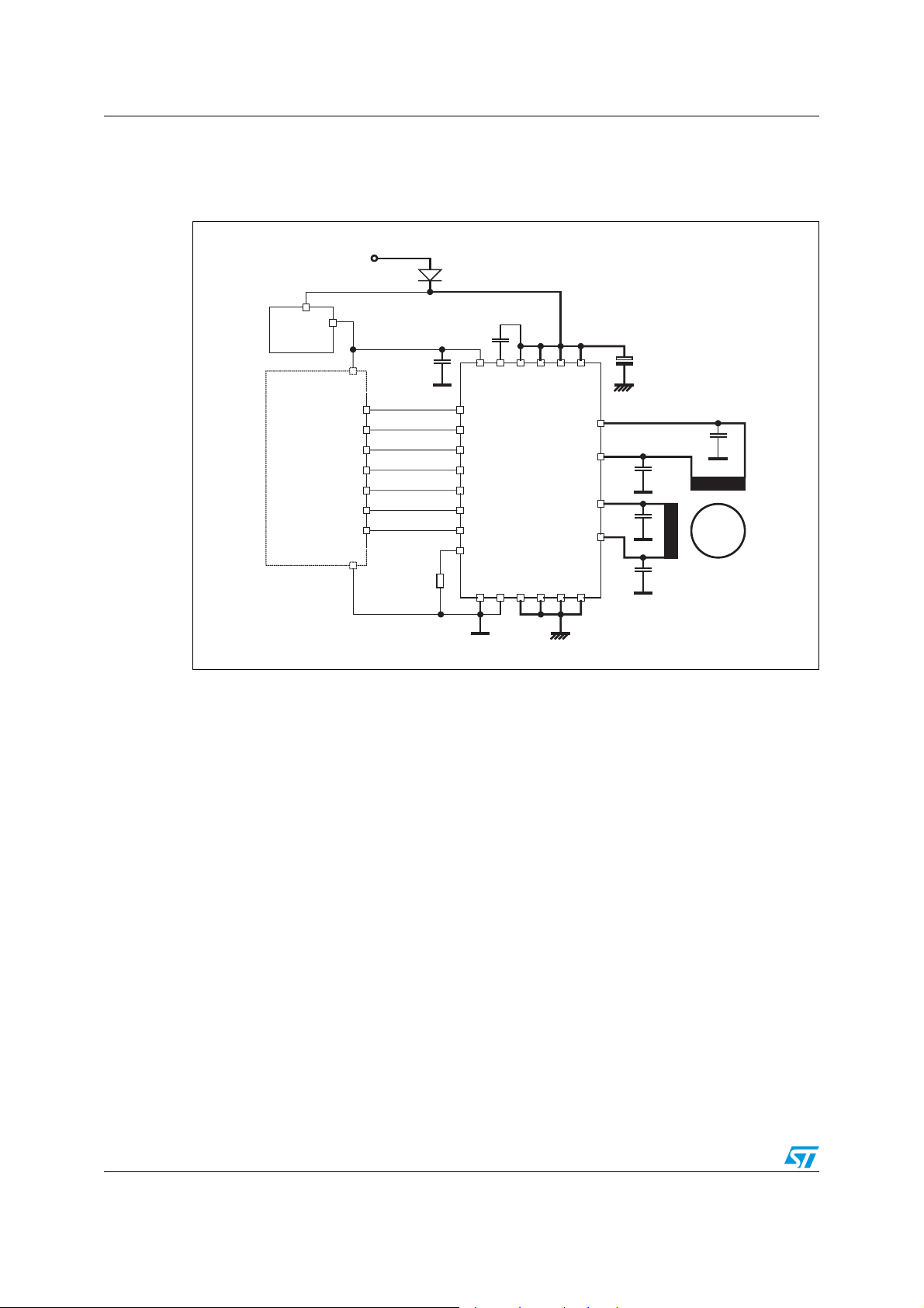
Figure 1. Application schematic diagram
V
bat
Vs
10
121
Vs
22
Vs
QA 1 2
QA 2
QB 1 11
QB 2
13 24
PGNDGND
C
buffer
23
2n2
2n2
14
2n2
2n2
SM
5V
V
reg
100n
out
out
in
µC
in
out
out
out
6k8
100n
19
16 15
Vcc
CP
STEP9
EN
21
PWM8
DO7
DI5
CLK4
CSN6
RREF
20
TEST
GND
1817
3
L9942
PGND PGND
The L9942 is driven by a microcontroller via the SPI (DO, DI, CLK, and CSN), STEP and EN
pins. Additional information is provided from the PWM pin.
The stepper motor driver is supplied from a 5 V voltage regulator and the reverse polarity
protected Vs. It is necessary to use a stabilization capacitor (with a minimum value of
minimum 100 nF) as close as possible at the Vcc pin. For the stabilization of the Vs supply
pin and to absorb motor energy, an electrolytic capacitor C
, with a minimum value as
buffer
calculated in Section 1.1, must be used.
Because the motor currents are supplied via the Vs-pins, all Vs-pins must have a low ohmic
connection to the supply voltage Vs. For the same reason, all GND and PGND pins must
have a low ohmic connection to the system ground. A star ground concept with separate
lines for GND and PGND is recommended.
At the charge pump pin, a capacitor with 100 nF to Vs is recommended.
To improve the EMI behavior, it is recommended to have 2.2 nF capacitors as close as
possible to the motor output pins, Qxy. Short motor connection wires also improve the EMI
behavior.
The internally-used reference voltage depends upon the value of the reference resistor,
positioned between the pin RREF and GND. Consequently, the precision of the L9942
depends upon the value of the reference resistor. One possible value for this resistor is
6.8 kΩ.
6/24
Page 7

AN2560 Typical application schematic
Due to the structure of the BCD process, the slug of the device is connected internally to
PGND and must also be connected externally to PGND.
1.1 Calculation of the buffer capacitor C
The stepper motor driver L9942 is usually designed in an environment similar to that shown
in Figure 1.
During motor operation, electrical energy is stored in the motor coils. If the motor shuts
down, this energy is fed back to the supply voltage Vs. Thus, there is a voltage increase at
Vs, which may cause an electrical overstress of the L9942. To avoid damage to the L9942,
the value of the buffer capacitor C
The energy balance can be calculated from:
motor
buffer
2
V
s1
2
⋅+ V
L
------------------ -
C
1
---
C
⋅⋅
bufferVs1
2
L
2
------------------ -
V
s1
C
V
s2
1
-- -
2
2
I
motor
motor
buffer
L
motorImotor
=
⋅+=
I
2
2
s2
2
motor
From this equation, it is possible to conclude:
● the voltage Vs2 must not exceed the maximum rating of the L9942
● if an over voltage shut down must be avoided, the voltage Vs2 must not exceed the
minimum over voltage threshold.
must be chosen carefully.
buffer
1
-- -
⋅⋅≈⋅⋅+
C
bufferVs2
2
2
buffer
Note: As a general recommendation, STMicroelectronics recommend a minimum buffer capacitor
of 47 µF. The ripple at Vs during normal motor operation should be between 5% and 10%.
7/24
Page 8
Typical application schematic AN2560
1.2 Low drop reverse polarity protection
Figure 2. Low drop reverse polarity protection
V
bat
100k
STD17NF03LT4
100k
Vs
100n
310 2216 15
VsCP Vs
C
buffer
L9942 Vreg
L9942
As shown in Figure 2 the charge pump pin can be used for a low drop reverse polarity
protection. The charge pump pin can also be used for other devices in the same application.
Because of the additional gate capacity, the charge pump ramps up more slowly than
without the additional MOSFET gate.
8/24
Page 9

AN2560 Shorted coil detection
2 Shorted coil detection
During free-wheeling time, the L9942 can use several decay modes that are programmable
by the SPI.
However, only on Auto decay, fast decay without delay time it is possible to detect
shorted coil because, during free-wheeling time, both opposite transistors (HS and LS) are
switched on and high current can rise. During free wheeling the current in the output stage is
monitored, but not regulated, with PWM. Because of this, the short overcomes the over
current filter time and can be detected.
In other decay modes, the decay can periodically change during wheeling of the motor (for
example, every 200 ms) to Auto decay, fast decay without delay time for few microseconds
and than change it back to previous value. This can be done in one clock step.
The decay mode cannot be changed at all values of the phase counter because fast decay
is not active during the whole period but only during decreasing current phase in the coil
(during the rising current phase, the coil is active slow decay mode).
A detailed explanation of Auto decay, fast decay without delay time for all step modes is
given in Figure 3.
Figure 3. Stepping modes (Auto decay mode, fast decay without delay time)
Phase Counter
Current
Dr iv e r A
Current
Dr iv e r B
Step CLK
Phase Counter
Current
Dr iv e r A
Current
Dr iv e r B
Step CLK
Phase Counter
Current
Dr iv e r A
Current
Dr iv e r B
Step CLK
Phase Counter
Current
Dr iv e r A
Current
Dr iv e r B
Step CLK
Full -Step Mode, DIR=0 Full -Step Mode, DIR=1
0 8 16 24
Fast Decay
Slo w Dec ay
0088
Fast Decay
0 4 8 1216202428
04 48
Slo w Dec ay
Fast Decay
024681012141618202224262830
0246 024624624688
Slo w Dec ay
Fast Decay
012345678910111213141516171819202122232425262728293031
01234567 012345671234567123456788
Slo w Dec ay
Fast Decay
HSB1
Slo w Dec ay
Fast Decay
Slo w Dec ay
0880
Half-S tep Mode, DI R=0
Slo w Dec ay
04 48
Fast Decay
0484
Slo w Dec ay
Fast Decay
Mini -Step Mode, DIR=0 Mini -Step Mode, DIR=1
Slo w Dec ay
Fast Decay
02468 246 02468 246
Fast Decay
Slo w Dec ay
Micro-St ep Mode, DIR=0
HSA2
Slo w Dec ay
Fast Decay
HSB2
012345678 12345678 01234567 1234567
Slo w Dec ay
Fast Decay
Fast Decay
Slo w Dec ay
Fast Decay
Slo w Dec ay
0484
Fast Decay
Slo w Dec ay
Fast Decay
HSA1
Slo w Dec ay
Phase Counter
Current
Dr iv e r A
Current
Dr iv e r B
Step CLK
Phase Counter
Current
Dr iv e r A
Current
Dr iv e r B
Step CLK
Phase Counter
Current
Dr iv e r A
Current
Dr iv e r B
Step CLK
Phase Counter
Current
Dr iv e r A
Current
Dr iv e r B
Step CLK
Slo w Dec ay
Fast Decay
Half-S tep Mode, DI R=1
Slo w Dec ay
Fast Decay
Slo w Dec ay
Fast Decay
Slo w Dec ay
Micro-St ep Mode, DIR=1
Slo w Dec ay
Fast Decay
HSB1
Fast Decay
Slo w Dec ay
Fast Decay
Slo w Dec ay
Fast Decay
Fast Decay
HSA1
Slo w Dec ay
Slo w Dec ay
Fast Decay
0880
Slo w Dec ay
Fast Decay
Slo w Dec ay
Fast Decay
Slo w Dec ay
HSB2
Fast Decay
04840484
0246824602468246
01234567812345678012345671234567
081624
Fast Decay
0088
Slo w Dec ay
Fast Decay
Slo w Dec ay
Fast Decay
Slo w Dec ay
HSA2
Fast Decay
Slo w Dec ay
0481216202428
04480448
024681012141618202224262830
02460246246 24688
012345678910111213141516171819202122232425262728293031
01234567012345671234567 123456788
Tabl e 1 shows Phase Counter values where fast decay is active.
9/24
Page 10

Shorted coil detection AN2560
Table 1. Phase counter values for fast decay
Step Mode Bridge DIR=0 DIR=1
(1)
Full step
A (8) (24) (16
B (0) (16) (24
A (8, 12) (24, 28 (20, 16
Half step
B (0, 4) (16, 20) (28, 24
A (8, 10,12,14) (24,26,28,30) (22,20,18,16
Mini step
B (0, 2, 4, 6) (16,18,20,22) (30,28,26,24
A
(8,9,10,11,12,13,14,15)
(24,25,26,27,28,29,30,31)
Micro step
B
1. Current profile_0 must be greater than 0
(16,17,18,19,20,21,22,23)
(0, 1, 2, 3, 4, 5, 6, 7)
(23,22,21,20,19,18,17,16
(7, 6, 5, 4, 3, 2, 1, 0
(31,30,29,28,27,26,25,24
(15,14,13,12,11,10, 9, 8
(1)
) (0
)
(1)
(1)
) (8
)
(1)
(1)
(1)
(1)
(1)
) (4, 0
) (12, 8
) (6, 4, 2, 0
) (14,12,10, 8
(1)
)
(1)
)
(1)
)
(1)
)
(1)
)
)
(1)
)
(1)
)
2.1 Conclusion
To detect shorted coil in both bridges (A and B) and for all step modes (Full, Half, Mini and
Micro), it is necessary to change decay mode to Auto decay, fast decay without delay time at
phase counter values of 0 and 8 (or 16 and 24). For the opposite direction, DIR=1 can also
use 0 and 8 (or 16 and 24) but the amplitude of current profile_0 must be greater than 0.
This configuration is illustrated in Figure 4.
Figure 4. Auto decay, fast decay without delay time at phase 0 and 8
200ms
123456789 1 01 1121 31 4151 61 7181 92 0212 22 3242 52 6272 82 9303 1
phase
0
01234567 012345671234567123456788
012345678 12345678 01234567 1234567
Auto decay, fas t dec ay without delay time at phase 0 and 8 (DIR=0)
01234 1516171819202122232425262728293031
01234 01123456712345678
456787801234567 1234567
123456789 1 01 1121 31 4151 61 7
0
01234567 012345678
012345678 12345678
Note: Another possibility is to change the decay mode for Micro, Mini and Half Step mode at
phase counter values of 4 and 12 and for Full Step mode at phase counter values of 0 and
8.
10/24
Page 11

AN2560 SPI
3 SPI
3.1 Fault bit
Figure 5. SPI transfer timing diagram
CSN high to low: DO enabled
CSN
t
CSN_HI,min
time
CLK
DI
DO
Control and Status Register
1234 56789101101213141510
DI: data will be accepted on the rising edge of CLK signal
A1 A0 D12D11 D10 D9D8D7 D6 D5 D4A2 D3 D2 D1 D0
DO: data will change on the falling edge of CLK signal
D12D11 D10 D9 D8 D7 D6 D5 D4 D3 D2 D1 D0
fault bit
actual data
status information
CSN low to high: actual data is
transfered to registers
old data
The first three bits of an SPI write frame are the register address. Thus, during this time, it is
not clear which register has to be written and read. This time is used at the DO-pin to
monitor the or-function of all diagnostic functions.
The register read out is started with the third falling edge of the SPI CLK. The read out is
finished 13 falling edges later and during the remaining time, until CSN is set to high, the orfunction of all diagnostic functions is monitored again.
Using this method, the failure status of the device can be checked without an SPI
communication. CSN is only pulled to low for a short while.
3.2 SPI communication monitoring
time
new data
A2 A1
time
D0
fault bit
actual data
time
time
SPI communication monitoring is described in the specification.
However, for register 0 the following two points should be considered.
1. During SPI communication, monitoring the STEP-pin must not be used. This could
cause the Phase Counter to be modified.
2. When not using the microstepping step mode, not all Current Profile Registers are
used. When sending a command to the Control Register 0 for SPI communication
monitoring with a Phase Counter value that not used in the selected step mode, the
device will correct the Phase Counter value itself. In this case, SPI communication
monitoring will fail.
11/24
Page 12

Decay modes AN2560
4 Decay modes
During the ON phase the current in the motor coil increases. After an ON phase, an OFF
phase follows that always starts with the cross current protection time (tcc).
The cross current protection time is automatically chosen with the slew rate and is typically
in the range from 0.5 to 4 µs.
After the cross current protection time, a programmed decay mode follows.
The basic decay modes of the stepper motor driver L9942 are:
● slow decay
● fast decay
● advanced decay modes, which are combinations of the slow and fast decay modes.
4.1 Slow decay
The slow decay mode realizes a minimum loss of energy in the motor coil. This means the
current decrease in the motor coil is “slow”.
Slow decay is illustrated in Figure 6.
Figure 6. Slow decay
I
L
„ON“
increase
I
L
Vs
ON
I
L
OFF
OFF
ON
cross current
protection
OFF
OFF
t
CC
t
slow
decay
Vs
BE
U
I
L
OFF
OFF
ON
OFF
Vs
Ron
ON
U
I
L
OFF
gnd
12/24
gnd
gnd
Page 13

AN2560 Decay modes
4.2 Fast Decay
The fast decay mode realizes a maximum loss of energy in the motor coil. This means the
current decrease in the motor coil is “fast”.
Fast decay is illustrated in Figure 7.
Figure 7. Fast decay
I
L
„ON“
increase
I
L
Vs
ON
OFF
I
L
gnd
OFF
ON
4.3 Advanced decay modes
With the stepper motor driver L9942, it is possible to combine the basic decay modes, slow
and fast decay.
4.3.1 Mixed decay
t
CC
cross current
protection
Vs
BE
OFF OFF
OFF
I
L
gnd
OFF
U
OFF
ON
fast
decay
t
Vs
Ron
ON
U
I
L
OFF
gnd
From the current point of view, for stepping down it is necessary to reduce the current in the
motor coil quickly. Therefore, a mostly slow decay is not useful because there is the danger
that the current in the motor coil does not reach the new (lower) current target. With fast
decay, the current undershoot may be stronger than necessary; this generates more EMI
than necessary.
A better result is obtained by mixing fast decay with slow decay. Mixed decay starts with fast
decay and switches to slow decay; the point for switching between the decay modes is
programmable. Mixed decay is shown in Figure 8.
13/24
Page 14

Decay modes AN2560
Figure 8. Mixed decay
I
● Mixed decay, fast decay until current undershoot
L
I
Target
t
t
CC
MD
I
II
t
In Figure 8, this behavior is shown with graph “I”. Fast decay is driven until the motor
coil current has undershot the target current and switches to slow decay until the end of
the phase.
● Mixed decay, fast decay until t
In Figure 8, this behavior is shown with graph “II”. The time t
cross current protection time tcc is over. After t
switches to slow decay. t
is programmable to 4µs or 8µs.
MD
> 4(8) µs
MD
is started after the
is finished the stepper motor driver
MD
MD
4.3.2 Auto decay
If the current in the motor coil is required to increase from step to step, it is sensible to save
the current in the motor coil. Therefore, the best decay mode is slow decay (see
Section 4.1).
If, on the other hand, the current in the motor coil should decrease from step to step, it is
sensible to reduce the current in the motor coil in a controlled way, as described in
Section 4.3.1. Therefore, the best decay mode is mixed decay.
The combination of slow decay for increasing current from step to step and mixed decay for
decreasing current from step to step is auto decay. A combination of slow decay and pure
fast decay is also possible but this option usually increases the EMI emission.
In Figure 9, auto decay is shown for one of the motor coils with micro stepping. For each
step, the appropriate current profile register is also shown.
Internally, a pointer moves from a current profile register to the next current profile register
with each StepCLK pulse. This start from the register 0 and goes step by step to register 8
and then back to register 0...
When the pointer is going in the direction from register 0 to 8, the L9942 uses slow decay.
When the pointer is going from register 8 to 0, mixed or fast decay is selected.
14/24
Page 15

AN2560 Decay modes
Figure 9. Auto decay
I
L
auto decay
fast or mixed
decay
t
t
012345678 1234567
slow decay
auto decay
StepCLK
V
current profile register
fast or mixed
slow decay
012345678 1234567
decay
● Auto decay, fast decay without delay time
Slow decay for current profile register going up (0 J 8) plus pure fast decay (see also
fast decay in Figure 7) for current profile register decreasing (8 I 0).
● Auto decay, fast decay until t
> 4(8) µs:
MD
Slow decay for current profile register going up (0 J8) plus mixed decay (see also
mixed decay in Figure 8, graph “II”) for current profile register decreasing (8 I0).
● Auto decay, fast decay until current undershoot
Slow decay for current profile register going up (0 I 8) plus mixed decay (see also
mixed decay in Figure 8, graph “I”) for current profile register increasing (0 J8).
15/24
Page 16

Stall detection AN2560
5 Stall detection
The stall detection function of the L9942 uses the reference drive of a stepper motor system,
such as that usually used in the start up phase of a front light levelling system.
5.1 Internal functionality (simplified)
The back EMF of the permanent magnetic rotor of the stepper motor is the effect that is
used for the stall detection function.
If the motor is turning “fast”, the back EMF is “high”. Thus, the voltage drop at the motor coils
is “low”. Combined with the inductance of the motor coils, it takes a “long” time to reach the
target current. Consequently, this means a “long” duty cycle of the pulse width modulation
(PWM).
If the motor is stopped mechanically, the back EMF is zero. Thus, the voltage drop at the
motor coils is “high”. Combined with the inductance of the motor coils, it takes a “short” time
to reach the target current. This means a “short” duty cycle of the PWM.
As is shown in Figure 10, an internal counter counts the duty cycle of the current regulation
PWM. This value is compared with a value given from the microcontroller via the SPI. If this
value is less than the one supplied by the microcontroller, the stall detection bit is set.
Figure 10. Stall detection function overview
I
L
PWM
PWM current
regulation
t
001000
From SPI
010011
for cur. reg.
counting
duty cycle
comp.
t
stall detection bit
16/24
Page 17

AN2560 Stall detection
5.2 How to determine the stall threshold at bench test
There are four steps to determine the stall threshold.
1. Drive motor in an environment with parameters as in a possible stall situation.
2. Run the motor so that it is turning continually and increase the stall threshold step by
step until the stall bit is set. This stall threshold value is called the “high value”.
3. With the same electrical conditions as before, stop the motor mechanically. Decrease
the stall threshold from the “high value”. After some steps the stall bit is reset. This stall
threshold value is called the “low value”.
4. The stall threshold is the middle value between the “high value” and the “low value”.
17/24
Page 18

Duty cycle for current regulation AN2560
6 Duty cycle for current regulation
The duty cycle for current regulation is always switched on for a minimum time and has a
maximum time of less than 100%.
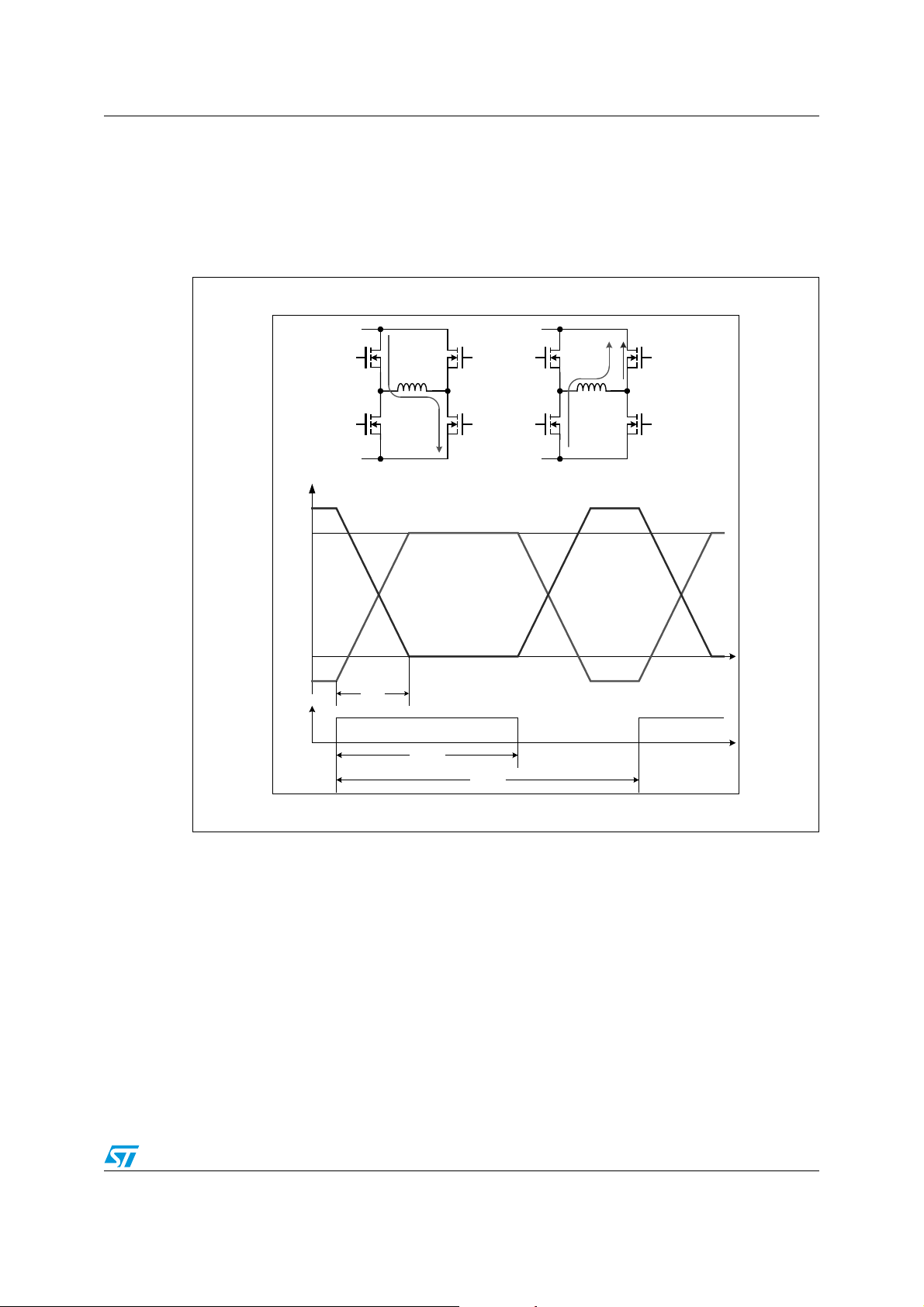
6.1 Minimum duty cycle
The minimum duty cycle is the sum of the “Glitch filter delay time”, the “Slew rate” and the
“Cross current protection time”. The “Slew rate” and the “Cross current protection time” are
programmed with the same bits.
6.2 Maximum duty cycle
The maximum duty cycle is less then 100%. The negligible off time is related to the “Cross
current protection time”. “Cross current protection time” is illustrated in Figure 11.
Figure 11. Cross current protection time and slew rate for maximum DC
OUT
ON
Slew Rate B
OFF
Slew Rate A
t
T
CC
t
18/24
Page 19
AN2560 Power dissipation
7 Power dissipation
The calculation of the power dissipation depends upon the selected slew rate and decay
mode of the device. In Figure 12 the set up was selected with a fast decay.
Figure 12. Current flow and voltage drop during fast decay
V
OUT-A
V
OUT-B
PWM
Vs
ON
OUT-B
OFF
Vs
I
L
OFF
OUT-A OUT-A
ON
gnd
OFF
OUT-B
ON
Vs
Ron
ON
U
I
L
OFF
gnd
ON FW fast decay
t
t
r/f
t
Pulse
t
D
t
For a rough calculation of the power dissipation, three different phases are selected:
1. static ON
2. static free wheeling (FW), fast decay
3. dynamic on and off with slew rate.
7.1 Static ON
Only the RDS,on of the high and low side switches are used for generating power
dissipation.
19/24
Page 20

Power dissipation AN2560
7.2 Static freewheeling
Only the RDS,on of the high and low side switches are used for free wheeling and
generating power dissipation.
7.3 Dynamic slew rate power dissipation
During the H-bridge switching, the voltage and the current chang in a triangular form with
the defined slew rate.
7.4 Power dissipation for one PWM phase
The temporary power dissipations, explained above, are summed for the complete PWM
phase.
PP
ON
PP
ON
P2R
DS ON,
t
Pulstr
--------------------------- - P
f⁄–
t
D
FW
tD2trf⁄⋅–
---------------------------- 2P
t
D
2
I
⋅⋅+⋅=
tD2trf⁄⋅–
----------------------------
⋅ UI
t
D
tDt
Pulstr
--------------------------------------- P
t
D
trf⁄
-------- -
SR
t
D
t
f⁄
r
-------- -
⋅⋅+⋅⋅=
t
D
f⁄––
SR
2trf⁄⋅
---------------- -
⋅+⋅+⋅=
t
D
20/24
Page 21

AN2560 PCB footprint proposal
8 PCB footprint proposal
Figure 13. Power SSO24 solder mask layout (all values in mm)
21/24
Page 22

PCB footprint proposal AN2560
Figure 14. Power SSO24 solder mask opening (all values in mm)
22/24
Page 23

AN2560 Revision history
9 Revision history
Table 2. Document revision history
Date Revision Changes
2-Nov-2007 1 Initial release.
23/24
Page 24

AN2560
Please Read Carefully:
Information in this document is provided solely in connection with ST products. STMicroelectronics NV and its subsidiaries (“ST”) reserve the
right to make changes, corrections, modifications or improvements, to this document, and the products and services described herein at any
time, without notice.
All ST products are sold pursuant to ST’s terms and conditions of sale.
Purchasers are solely responsible for the choice, selection and use of the ST products and services described herein, and ST assumes no
liability whatsoever relating to the choice, selection or use of the ST products and services described herein.
No license, express or implied, by estoppel or otherwise, to any intellectual property rights is granted under this document. If any part of this
document refers to any third party products or services it shall not be deemed a license grant by ST for the use of such third party products
or services, or any intellectual property contained therein or considered as a warranty covering the use in any manner whatsoever of such
third party products or services or any intellectual property contained therein.
UNLESS OTHERWISE SET FORTH IN ST’S TERMS AND CONDITIONS OF SALE ST DISCLAIMS ANY EXPRESS OR IMPLIED
WARRANTY WITH RESPECT TO THE USE AND/OR SALE OF ST PRODUCTS INCLUDING WITHOUT LIMITATION IMPLIED
WARRANTIES OF MERCHANTABILITY, FITNESS FOR A PARTICULAR PURPOSE (AND THEIR EQUIVALENTS UNDER THE LAWS
OF ANY JURISDICTION), OR INFRINGEMENT OF ANY PATENT, COPYRIGHT OR OTHER INTELLECTUAL PROPERTY RIGHT.
UNLESS EXPRESSLY APPROVED IN WRITING BY AN AUTHORIZED ST REPRESENTATIVE, ST PRODUCTS ARE NOT
RECOMMENDED, AUTHORIZED OR WARRANTED FOR USE IN MILITARY, AIR CRAFT, SPACE, LIFE SAVING, OR LIFE SUSTAINING
APPLICATIONS, NOR IN PRODUCTS OR SYSTEMS WHERE FAILURE OR MALFUNCTION MAY RESULT IN PERSONAL INJURY,
DEATH, OR SEVERE PROPERTY OR ENVIRONMENTAL DAMAGE. ST PRODUCTS WHICH ARE NOT SPECIFIED AS "AUTOMOTIVE
GRADE" MAY ONLY BE USED IN AUTOMOTIVE APPLICATIONS AT USER’S OWN RISK.
Resale of ST products with provisions different from the statements and/or technical features set forth in this document shall immediately void
any warranty granted by ST for the ST product or service described herein and shall not create or extend in any manner whatsoever, any
liability of ST.
ST and the ST logo are trademarks or registered trademarks of ST in various countries.
Information in this document supersedes and replaces all information previously supplied.
The ST logo is a registered trademark of STMicroelectronics. All other names are the property of their respective owners.
© 2007 STMicroelectronics - All rights reserved
STMicroelectronics group of companies
Australia - Belgium - Brazil - Canada - China - Czech Republic - Finland - France - Germany - Hong Kong - India - Israel - Italy - Japan -
Malaysia - Malta - Morocco - Singapore - Spain - Sweden - Switzerland - United Kingdom - United States of America
www.st.com
24/24
 Loading...