

Page 1
AN2648
Application note
Increasing the resolution of analog temperature sensors
Introduction
For a recent trade show, a demonstration board was required to display ST's new low-cost
temperature sensor, the STLM20. The idea was to connect it to a basic microcontroller with
on-board analog-to-digital converter (ADC) and display the temperature on seven-segment
LEDs. Any user would be able to affect the temperature by applying his finger directly to the
sensor and then watch the display change as a result.
The goal was to keep things simple and use the ADC converter on the micro thus avoiding
the expense and engineering effort of using an external ADC.
Using the STLM20 temperature sensor with low-cost microcontrollers
The design flow used for the demonstration board can be applied in many applications. This
document describes how any user can implement a temperature sensor design using the
LM20 and a low-cost microcontroller with integral A-D converter.
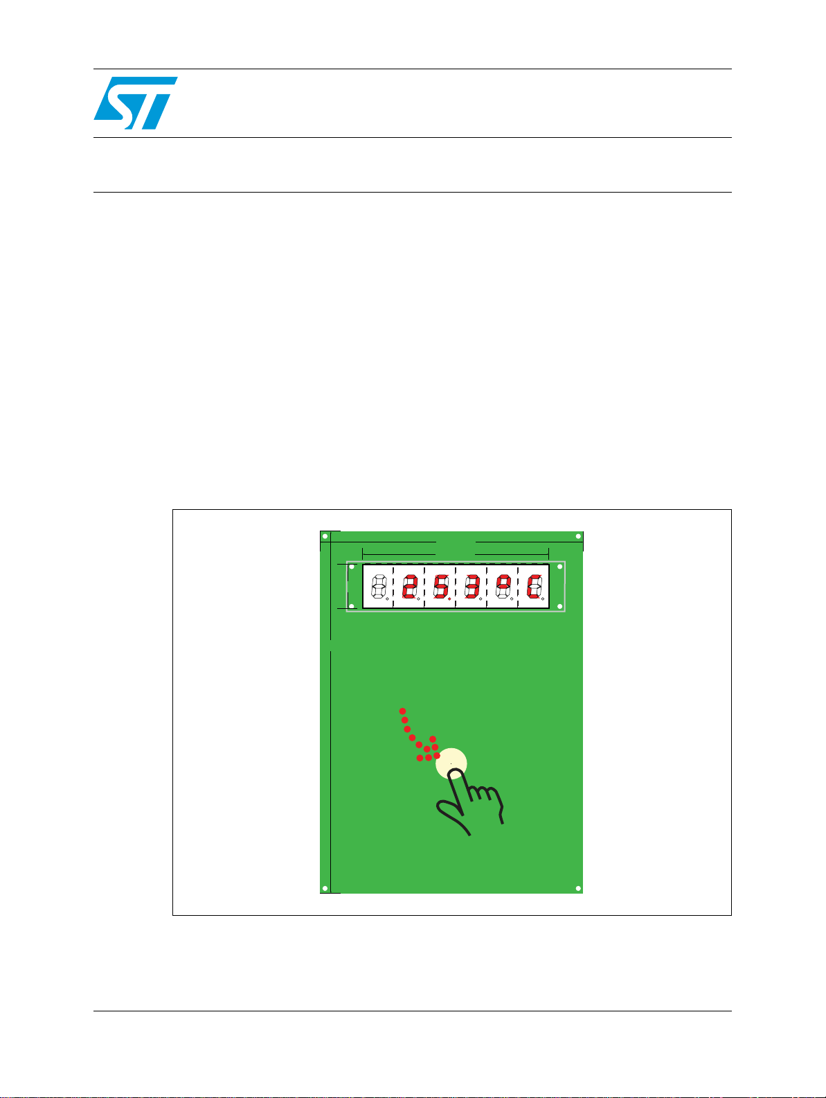
Figure 1. STLM20 demonstration board
34mm / 1.34
280mm / ~11
200mm / ~8
144mm / 5.7
December 2007 Rev 1 1/15
www.st.com
Page 2
STLM20 temperature-to-output transfer function AN2648
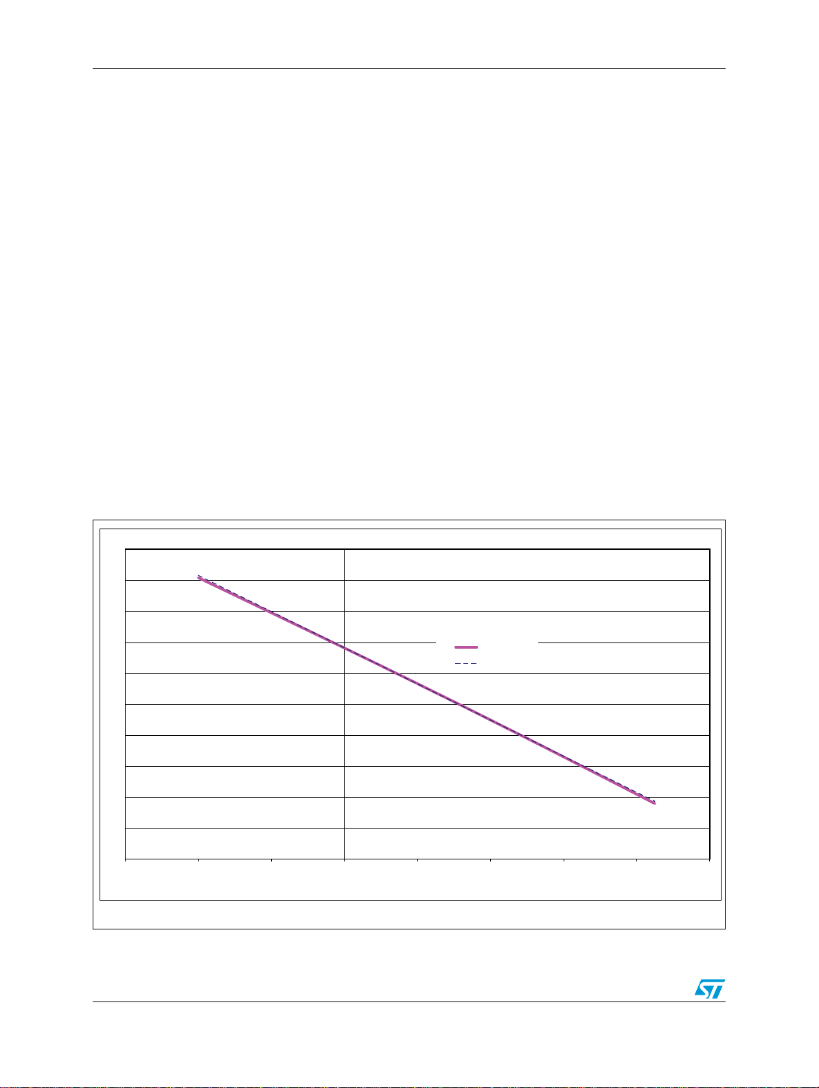
1 STLM20 temperature-to-output transfer function
Upon examining the temperature sensor's output characteristics, several issues become
apparent. The STLM20 is a voltage output device with a 2
0
This is rather unwieldy math for a simple 8-bit micro, but a linear approximation is available
which matches the curve very closely. As shown in Figure 2, the dashed blue line is a very
good fit to the pink parabola of the 2
Equation 1
This is much more manageable for coding in assembly language without a math package. In
this figure, the reader will note that the curve deviates only slightly from the line at the
extreme ends. In the middle, they are almost indistinguishable.
Figure 2. STLM20 transfer function
nd
order transfer function:
226
−−
nd
order equation above, and has the following equation:
0
2.5
+×°−=
+××−+××−=
V8663.1TC)V/01169.0(V
V8639.1)T1015.1()T1088.3(V
2.3
2.1
, (V)
O
Output voltage, V
-60 -40 -20 0 20 40 60 80 100
1.9
1.7
1.5
1.3
1.1
0.9
0.7
0.5
2nd Order
Linear
Temperature, T (˚C)
ai13986
2/15
Page 3
AN2648 STLM20 temperature-to-output transfer function
The second issue arises with the output voltage range. The micro's ADC performs ratiometric conversion on the input using V
respectively. That means that when the input voltage equals V
be 255 (FF
the range V
), and when the input is ground, the output will be 0 (00
HEX
to ground is converted proportionally according to the following relationship:
CC
and ground as the upper and lower references,
CC
CCIN
, the 8-bit ADC's output will
CC
552)/VV((dec)output ADC
×=
). Any voltage in
HEX
For this application, the nominal VCC is 5 V, so this equation becomes:
51V552/5)V((dec)output ADC
×=×=
ININ
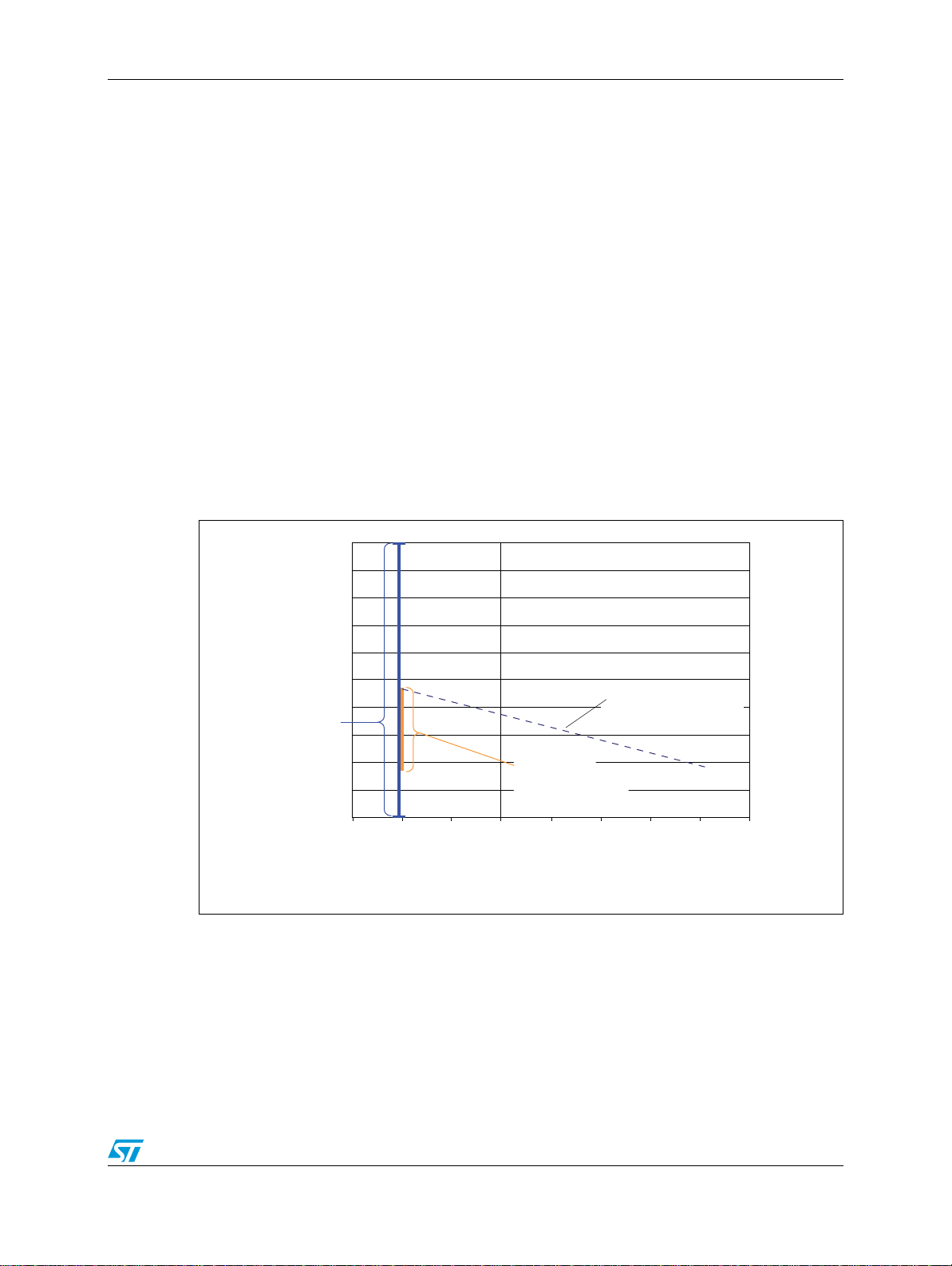
Referring to Figure 3, while the ADC can accept inputs over the full range 0 to 5 V, the
temperature sensor output will vary over a much smaller range, between 0.87 and 2.33 volts
across the temperature range –40° to +85°C.
Figure 3. STLM20 output voltage range
5
Available
voltage
range
(V)
O
Output voltage, V
-60 -40 -20 0 20 40 60 80 100
4.5
4
3.5
3
2.5
2
1.5
1
STLM20
output voltage
0.5
range
0
STLM20 full range,
linear, ind temp
Temperature, T (˚C)
ai13987
This amounts to using only 1.46 V of the available 5 V range. Furthermore, in the intended
demonstration board application, the necessary temperature range was approximately room
temperature –15°/+25°, or 10° to 50°C.
For this target temperature range, the voltage range is 1.28 to 1.75 V, an interval of less than
0.5 V, less than one tenth the available 5 V range. This is depicted in Figure 4.
3/15
Page 4
STLM20 temperature-to-output transfer function AN2648
/
Figure 4. Application temperature and voltage ranges
5
4.5
4
3.5
(V)
O
3
2.5
Temperature range of interest
2
Output voltage, V
1.5
Used voltage range
of application
1
STLM20 full temperature range
0.5
Available voltage range
0
-60 -40 -20 0 20 40 60 80 100
Temperature, T (˚C)
In Equation 1, the slope is –11.69 mV per °C. For the 8-bit ADC, the step size is 5 V/255
steps or 0.019608 V/step. Comparing this to the slope, we get:
V/step 0.019608
11690.0
This means that, with the temperature sensor connected directly to the ADC, the resolution
is only 1.68°C/step. The smallest temperature increment the ADC can resolve is
1.68°C. This is very coarse resolution.
4/15
ai13988
°−=
°−
CV
C/step1.677318
Page 5
AN2648 STLM20 temperature-to-output transfer function
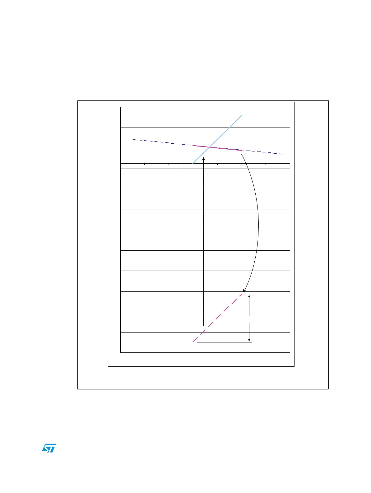
Given that the expected voltage range is less than 0.5 V, it should be possible to amplify the
STLM20 output signal so that is uses more of the available voltage range. A 10x
amplification should be possible without exceeding the available 5 V range. Furthermore, a
positive slope is more intuitive to the user, so inverting it would be helpful, too. Hence, a
gain of –10 should be used. Multiplying equation 1 by –10, we get the curve as shown at the
bottom in Figure 5.
Figure 5. Application transfer function after gain, inversion and offset
5.5
3.5
1.5
-50 -30 -10 10 30 50 70 90
-0.5
-2.5
-4.5
-6.5
+17.5
x –10
Voltage (V)
-8.5
-10.5
-12.5
-14.5
< 5V
-16.5
-18.5
Temperature, T (˚C)
ai13989
The result has positive slope and spans from –17.5 to –12.8, an interval of about 4.7 V,
much closer to the available 5 V range.
5/15
Page 6

STLM20 temperature-to-output transfer function AN2648
With an offset of approximately +17.5 V the curve is moved back into the range 0-5 V to give
the transfer function shown as the light blue line in Figure 5.
So how is this done? What circuit will perform this transformation without adding intolerable
cost to the system?
It turns out that a difference amplifier can be used to add gain and offset, and can do the
inversion as well. And it requires only one op-amp to implement.
An additional op-amp is used as a voltage follower out of the temperature sensor to prevent
output loading from affecting the STLM20's output level. The net amplifier requirement then
is a dual op-amp. A voltage reference is also required to provide the offset level going into
the difference amp. The overall circuit is shown in Figure 6.
The STLM20 output voltage, V
, appears identically at the first op-amp output. That then
0
drives the inverting input of the difference amp with a gain of –50k/5k = –10.
This translates the curve from a voltage range of 1.28 V to 1.75 V to a range of –12.8 V to
–17.5 V so an offset of about +17.5 V must be applied. The 1.7676 V reference sees a gain
of 10 (R4/R3 = ~50k/5k = 10) on the op-amp's non-inverting input. Thus, 17.676 volts is
added back into the translation.
With this gain and offset, the original curve, which had an interval of less than 0.5 V and a
negative slope, is transformed to one which spans close to 5 V and has a positive slope as
illustrated by the light blue line in Figure 5.
Figure 6. STLM20 with gain and offset circuit
V
CC
V
0.1uF
T
STLM20
V
CC
V
O
0.1uF
CC
0.1uF
LMV358
1.7676V
= V
O
R3
50k
R1
V
V
5k
1
R2
5k
2
LMV358
V
OUT
TS431
6/15
0.1uF
R4
50k
0.1uF
ai13990
Page 7

AN2648 STLM20 temperature-to-output transfer function
Equation 2 is the basic difference amplifier equation.
Equation 2
+
=
V
OUT
If R1 = R2 and R3 = R4, then it reduces to:
However, obtaining perfectly identical resistors is nearly impossible. Thus, the more
complex expression of Equation 2 is used. Starting with Equation 1 on page 2, for Figure 6,
we have:
O
In Figure 6, V1 is driven by V0, so Equation 2 becomes:
=
V
OUT
+
+
+
R4 R1) R3 ( V2
R1R2) (R4
R
)VV(V −=
12OUT
R
⋅−=
R4 R1) R3 ( V2
R1R2) (R4
R3V
⋅
1
−
R1
3
1
V 1.8663 + T 0.01169V
R3V
⋅
O
−
R1
Substituting the expression for V0 into this, we get:
R4 R1) R3 (
OUT
OUT
V2V
⋅=
+
+
V2V
⋅=
+
+
−
R1R2) (R4
R4 R1) R3 (
R1R2) (R4
7/15
⋅⋅−
R31.8663) + T 0.01169(
R1
R3
0.01169
1.8663 T
R1
⋅−⋅⋅+
R3
R1
Page 8

STLM20 temperature-to-output transfer function AN2648
Equation 3
V2V
OUT
The ADC inside the microprocessor is shown in Figure 7.
Figure 7. ADC in microprocessor
⋅=
+
+
R4 R1) R3 (
1.8663
R1R2) (R4
VCC = 5V
V
OUT
A/D
R3
R1
V
ADC
CPU
8-bit
MEM
MICROCONTROLLER
I/O
R3
0.01169
R1
ai13991
T
⋅⋅+⋅−
For the ADC output, we have the following, where INT means the integer portion of the
expression:
OUT
⎤
⎥
⎦
R3
R1
V
R3
R1
⎤
R3
0.01169
R1
R3
0.01169
⎞
⎟
T
⋅⋅+⋅−
⎥
⎟
⎠
⎦
T
⋅⋅+⋅−
R1
⎡
255
INTV
=
ADC
Substituting Equation 3, we get:
⎡
⎛
255
⎜
CC
V
CC
⎜
⎝
V2
V2
⋅=
⋅=⋅
INTV
ADC
⎢
⎣
Rearranging, and ignoring the integer notation for now, we get:
ADC
V
255
V
+
+
+
+
⎢
V
CC
⎣
R4 R1) R3 (
1.8663
R1R2) (R4
R4 R1) R3 (
1.8663
R1R2) (R4
8/15
Page 9

AN2648 STLM20 temperature-to-output transfer function
To get the measured temperature, T
ADC
ADC
V
255
V
CC
255
V
255
V
V
ADC
V
Equation 4
CC
CC
R1
R3
V2
R1
R3
⋅−⋅
+
+
V2
⋅−⋅⋅
V2
⋅−⋅⋅
V
V T T
ADCMEASA
CC
255
R4 R1) R3 (
R1R2) (R4
+
+
+
+
R1
R3
MEASA
1.8663
R4 R1) R3 (
R1R2) (R4
R4 R1) R3 (
R3R2) (R4
1
0.01169
, we must solve for T above:
R1
R3
R3
R1
1.8663
⋅−⋅⋅⋅==
V2
R3
R1
+
+
R1
R3
R3R2) (R4
R3
0.01169
R1
T 0.01169 1.8663
⋅=+
R4 R1) R3 (
T
⋅⋅=⋅+
1
0.01169
R3
0.01169
R1
+⋅
R1
R3
1.8663
0.01169
T
⋅⋅⋅=⋅⋅+⋅
This has the form:
Equation 4b
KKV T +⋅=
OSADCMEASA
But, rather than using this equation, it is better to filter the temperature, to average multiple
samples together for display. This has two benefits. It smoothes the changes resulting in a
displayed value which updates more gradually. And it increases the effective resolution of
the sensor. By adding two more bits, this essentially makes the A/D appear to have 10-bit
resolution.
So, we use a modified version of the previous math, but sum four consecutive samples
together:
⎛
⎜
⎜
⎝
OUT
V2
⎤
V
⎥
⎦
⎤
R4 R1) R3 (
⋅=
+
+
1.8663
R1R2) (R4
R3
R1
R3
0.01169
R1
⎞
⎟
T
⋅⋅+⋅−
⎥
⎟
⎠
⎦
⎡
255
INTV
=
ADC
ADC
⎢
V
CC
⎣
⎡
255
INTV
⎢
V
CC
⎣
9/15
Page 10

STLM20 temperature-to-output transfer function AN2648
V
= 4 samples of V
SUM4
, range 0 to 1020.
ADC
V
V
V
SUM4
SUM4
SUM4
SUM4
⎡
⎛
255
⎜
V
CC
⋅=⋅
⋅−⋅
⎜
⎝
V2
V2
⋅−⋅⋅
⋅⋅=
+
+
+
+
INT4V
⎢
⎣
Rearranging and ignoring the integer operator, we get:
V
CC
V2
1020
V
CC
V2
1020
V
1020
CC
R1
R3
+
+
R4 R1) R3 (
R1R2) (R4
R4 R1) R3 (
R1R2) (R4
+
+
R4 R1) R3 (
R1R2) (R4
1.8663
1.8663
R4 R1) R3 (
R1R2) (R4
1.8663
R3
R1
R3
R1
R1
R3
R3
R1
1.8663
R3
R1
0.01169
R3
R1
0.01169
R1
R3
R3
R1
⎤
R3
0.01169
R1
T
⋅⋅+⋅−
T
⋅⋅=⋅+
⎞
⎟
T
⋅⋅+⋅−
⎥
⎟
⎠
⎦
R1
R3
0.01169
R1
R3
T
⋅⋅⋅=⋅⋅+⋅
V
SUM4
Equation 5
Equation 5b
V
1020
R1
CC
V2
⋅−⋅⋅
R3
V
VT T
SUM4MEAS4
This is a linear equation and has the form:
CC
1020
K/4KV T +⋅=
+
+
R1
R3
OSSUM4MEAS4
R4 R1) R3 (
R3R2) (R4
1
0.01169
V2
⋅−⋅⋅⋅==
T 0.01169 1.8663
⋅=+
+
R4 R1) R3 (
+
R3R2) (R4
1
0.01169
1.8663
+⋅
0.01169
10/15
Page 11

AN2648 STLM20 temperature-to-output transfer function
Notice that the upper limit for the sum of four samples is 1020 (4 x 255) and not 1023 as
might be inferred for a 10-bit number.
The actual values of K
voltage reference output and V
board, we have these values:
For KS, we insert these values into Equation 4 and get this for a single sample:
ADCMEASA
/4 and KO depend on the four resistors in the difference amp, the
S
V
V T T
ADCMEASA
CC
255
. In the case of the temperature sensor demonstration
CC
5107R1
Ω=
5105 R2
Ω=
50850 R3
Ω=
50850 R4
Ω=
==
V2
V9058.4V
V 1.7676 V V2
⋅−⋅⋅⋅==
+
+
R4 R1) R3 (
R3R2) (R4
1
0.01169
=
CC
REF
R1
R3
8.437710.16528V T
+⋅=
1
0.01169
1.8663
+⋅
0.01169
Thus, for Equation 4b, KS = 0.16528 and KO = 8.43771. Therefore, KS/4 = 0.04132.
Substituting this into Equation 5b, we get:
8.43771 V0.04132 T
+⋅=
SUM4MEAS4
This gives the four-sample average of the temperature. However, more processing is still
required to get it into a form suitable for implementing in a simple processor. Since the
processor is an 8-bit, integer machine, multiplication by a real number - in this case a
fraction - is difficult and requires lots of math software.
Instead of doing such complicated math, it's easier to first multiply by 1000, then later divide
by 1000.
So, Equation 5b becomes:
8438 V41 T 1000
+⋅=⋅
SUM4MEAS4
11/15
Page 12

STLM20 temperature-to-output transfer function AN2648
Since the numbers are strictly integers, some truncation error has occurred. Running error
analysis on the calculated results shows an average error of –0.21°C, so as a final
adjustment, an additional 0.2(x1000) is added to get this equation:
8638 V412008438 V41 T 1000
+⋅=++⋅=⋅
SUM4SUM4MEAS4
The above equation is then implemented in the software. The final step is dividing the result
by 1000 and writing it to the demonstration board's display.
The overall solution looks like this (Figure 8):
Figure 8. Overall solution
V
CC
STLM20
TEMPERATURE
TO
VOLTAGE
VO = –11.69mV / ˚C × T + 1.8663V
slope is 0.01169
V
OUT
V
OUT
1.7676V
=
=
V
1
V
2
V
REF
V
/
˚C
R4 R1) R3 ( V2
+
R1R2) (R4
+
R4 R1) R3 (
+
V2 ••+•
•=
R1R2) (R4
+
0.1164 • T – 0.9821
R3R1
R2
R4
R3V
•
O
R1
ADC
=
V
CC
4.9058V
R3
T
0.01169
R1
255
V
INTV
=
OUT
V
CC
V
R1
CC
V•=+
ADC
255
T
= V
MEASA
T
= V
MEAS4
•
V2
••
R3
V
V T
ADCMEASA
255
•
0.165284 + 8.437709
ADC
•
0.041321 + 8.437709
SUM4
41
1000
+
R4 R1) R3 (
+
R3R2) (R4
1
R1
CC
R3
8438
+
1000
0.01169
V2
T 0.01169 1.8663
+
••••= T=
R4 R1) R3 (
+
R3R2) (R4
1
0.01169
1.8663
+•
0.01169
R3
1.8663
R1
V
OUT
A/D
CPU
I/O
8-bit
MEM
MICROCONTROLLER
ai13992
Thus, for the minor expense of a voltage reference and dual op-amp, the resolution has
been improved from 1.677°C per ADC step to better than 0.1°C steps on the display.
12/15
Page 13

AN2648 Summary
2 Summary
The STLM20 is very accurate over a wide temperature range and has a nearly linear output
which spans the voltage range 2.33 down to 0.87 volts over the corresponding temperature
range –40° to +85°C. While it can be directly connected to an 8-bit A-D converter such as
those often found integrated into low-cost microcontrollers, the resolution may be too coarse
for some applications, amounting to –1.677°C per A-D step. For applications requiring
higher resolution, users can use an op-amp and a voltage reference to add gain and offset
to the STLM20 output. This has the effect of increasing the resolution over the temperature
range of interest while avoiding the need for a more expensive, higher resolution A-D
converter. Using averages of four samples also increases the effective resolution. The final
result is that users can achieve resolution as fine as 0.1°C with the STLM20.
13/15
Page 14

Revision history AN2648
3 Revision history
Table 1. Document revision history
Date Revision Changes
20-Dec-2007 1 Initial release.
14/15
Page 15

AN2648
Please Read Carefully:
Information in this document is provided solely in connection with ST products. STMicroelectronics NV and its subsidiaries (“ST”) reserve the
right to make changes, corrections, modifications or improvements, to this document, and the products and services described herein at any
time, without notice.
All ST products are sold pursuant to ST’s terms and conditions of sale.
Purchasers are solely responsible for the choice, selection and use of the ST products and services described herein, and ST assumes no
liability whatsoever relating to the choice, selection or use of the ST products and services described herein.
No license, express or implied, by estoppel or otherwise, to any intellectual property rights is granted under this document. If any part of this
document refers to any third party products or services it shall not be deemed a license grant by ST for the use of such third party products
or services, or any intellectual property contained therein or considered as a warranty covering the use in any manner whatsoever of such
third party products or services or any intellectual property contained therein.
UNLESS OTHERWISE SET FORTH IN ST’S TERMS AND CONDITIONS OF SALE ST DISCLAIMS ANY EXPRESS OR IMPLIED
WARRANTY WITH RESPECT TO THE USE AND/OR SALE OF ST PRODUCTS INCLUDING WITHOUT LIMITATION IMPLIED
WARRANTIES OF MERCHANTABILITY, FITNESS FOR A PARTICULAR PURPOSE (AND THEIR EQUIVALENTS UNDER THE LAWS
OF ANY JURISDICTION), OR INFRINGEMENT OF ANY PATENT, COPYRIGHT OR OTHER INTELLECTUAL PROPERTY RIGHT.
UNLESS EXPRESSLY APPROVED IN WRITING BY AN AUTHORIZED ST REPRESENTATIVE, ST PRODUCTS ARE NOT
RECOMMENDED, AUTHORIZED OR WARRANTED FOR USE IN MILITARY, AIR CRAFT, SPACE, LIFE SAVING, OR LIFE SUSTAINING
APPLICATIONS, NOR IN PRODUCTS OR SYSTEMS WHERE FAILURE OR MALFUNCTION MAY RESULT IN PERSONAL INJURY,
DEATH, OR SEVERE PROPERTY OR ENVIRONMENTAL DAMAGE. ST PRODUCTS WHICH ARE NOT SPECIFIED AS "AUTOMOTIVE
GRADE" MAY ONLY BE USED IN AUTOMOTIVE APPLICATIONS AT USER’S OWN RISK.
Resale of ST products with provisions different from the statements and/or technical features set forth in this document shall immediately void
any warranty granted by ST for the ST product or service described herein and shall not create or extend in any manner whatsoever, any
liability of ST.
ST and the ST logo are trademarks or registered trademarks of ST in various countries.
Information in this document supersedes and replaces all information previously supplied.
The ST logo is a registered trademark of STMicroelectronics. All other names are the property of their respective owners.
© 2007 STMicroelectronics - All rights reserved
STMicroelectronics group of companies
Australia - Belgium - Brazil - Canada - China - Czech Republic - Finland - France - Germany - Hong Kong - India - Israel - Italy - Japan -
Malaysia - Malta - Morocco - Singapore - Spain - Sweden - Switzerland - United Kingdom - United States of America
www.st.com
15/15
 Loading...