

Page 1

AN2646
Application note
Smartcard interface with the STM8S microcontroller
Introduction
This document describes a firmware and hardware smartcard interface solution based on
the STM8 UART1 peripheral. The main purpose of this firmware and hardware package is to
provide resources that facilitate the development of an application using the UART1
peripheral in smartcard mode.
The firmware interface consists of library source files developed so as to support the
ISO 7816-3/4 specification. An application example is also provided.
This document and its associated firmware are available for download from the
STMicroelectronics website: www.st.com.
August 2008 Rev 2 1/43
www.st.com
Page 2

Contents AN2646 - Application note
Contents
1 Smartcard interface description . . . . . . . . . . . . . . . . . . . . . . . . . . . . . . . 4
1.1 Introduction . . . . . . . . . . . . . . . . . . . . . . . . . . . . . . . . . . . . . . . . . . . . . . . . 4
1.2 External interface . . . . . . . . . . . . . . . . . . . . . . . . . . . . . . . . . . . . . . . . . . . . 4
1.3 Protocol . . . . . . . . . . . . . . . . . . . . . . . . . . . . . . . . . . . . . . . . . . . . . . . . . . . 4
1.4 Smartcard clock generator . . . . . . . . . . . . . . . . . . . . . . . . . . . . . . . . . . . . . 5
2 Smartcard reader hardware connection . . . . . . . . . . . . . . . . . . . . . . . . . 6
3 ISO 7816 – protocol overview . . . . . . . . . . . . . . . . . . . . . . . . . . . . . . . . . 8
3.1 Introduction . . . . . . . . . . . . . . . . . . . . . . . . . . . . . . . . . . . . . . . . . . . . . . . . 8
3.2 ISO 7816-2 – pin location . . . . . . . . . . . . . . . . . . . . . . . . . . . . . . . . . . . . . . 8
4 ISO 7816-3 – electronic signal and transmission protocol . . . . . . . . . 10
4.1 Card power-up and reset . . . . . . . . . . . . . . . . . . . . . . . . . . . . . . . . . . . . . 11
4.2 Data transfer . . . . . . . . . . . . . . . . . . . . . . . . . . . . . . . . . . . . . . . . . . . . . . . 12
4.3 Answer to reset (ATR) . . . . . . . . . . . . . . . . . . . . . . . . . . . . . . . . . . . . . . . 16
5 ISO 7816-4 – smartcard commands . . . . . . . . . . . . . . . . . . . . . . . . . . . . 18
5.1 T0 protocol . . . . . . . . . . . . . . . . . . . . . . . . . . . . . . . . . . . . . . . . . . . . . . . . 18
5.2 Application-level protocols . . . . . . . . . . . . . . . . . . . . . . . . . . . . . . . . . . . . 20
5.2.1 The ISO 7816-4 APDU . . . . . . . . . . . . . . . . . . . . . . . . . . . . . . . . . . . . . 21
5.2.2 File system API . . . . . . . . . . . . . . . . . . . . . . . . . . . . . . . . . . . . . . . . . . . 22
5.2.3 ISO 7816-4 functions . . . . . . . . . . . . . . . . . . . . . . . . . . . . . . . . . . . . . . . 23
5.2.4 Security API . . . . . . . . . . . . . . . . . . . . . . . . . . . . . . . . . . . . . . . . . . . . . . 24
6 Smartcard interface library: description . . . . . . . . . . . . . . . . . . . . . . . . 26
6.1 File organization . . . . . . . . . . . . . . . . . . . . . . . . . . . . . . . . . . . . . . . . . . . . 26
6.2 Smartcard interface library functions . . . . . . . . . . . . . . . . . . . . . . . . . . . . 26
6.2.1 SC_Handler function . . . . . . . . . . . . . . . . . . . . . . . . . . . . . . . . . . . . . . . 27
6.2.2 SC_PowerCmd . . . . . . . . . . . . . . . . . . . . . . . . . . . . . . . . . . . . . . . . . . . 30
6.2.3 SC_Reset . . . . . . . . . . . . . . . . . . . . . . . . . . . . . . . . . . . . . . . . . . . . . . . 30
6.2.4 SC_ParityErrorHandler . . . . . . . . . . . . . . . . . . . . . . . . . . . . . . . . . . . . . 31
6.2.5 SC_PTSConfig . . . . . . . . . . . . . . . . . . . . . . . . . . . . . . . . . . . . . . . . . . . 31
2/43
Page 3

AN2646 - Application note Contents
6.3 How to send APDU commands to the smartcard . . . . . . . . . . . . . . . . . . . 32
6.3.1 SC_GET_A2R . . . . . . . . . . . . . . . . . . . . . . . . . . . . . . . . . . . . . . . . . . . . 32
6.3.2 SELECT_FILE . . . . . . . . . . . . . . . . . . . . . . . . . . . . . . . . . . . . . . . . . . . . 32
6.3.3 SC_GET_RESPONSE . . . . . . . . . . . . . . . . . . . . . . . . . . . . . . . . . . . . . 32
6.3.4 SC_READ_BINARY . . . . . . . . . . . . . . . . . . . . . . . . . . . . . . . . . . . . . . . . 33
6.3.5 SC_CREATE_FILE . . . . . . . . . . . . . . . . . . . . . . . . . . . . . . . . . . . . . . . . 33
6.3.6 SC_UPDATE_BINARY . . . . . . . . . . . . . . . . . . . . . . . . . . . . . . . . . . . . . . 34
6.3.7 SC_VERIFY . . . . . . . . . . . . . . . . . . . . . . . . . . . . . . . . . . . . . . . . . . . . . . 34
6.4 Parity error management . . . . . . . . . . . . . . . . . . . . . . . . . . . . . . . . . . . . . 35
6.4.1 Data sent from card to reader . . . . . . . . . . . . . . . . . . . . . . . . . . . . . . . . 35
6.4.2 Data sent from reader to card . . . . . . . . . . . . . . . . . . . . . . . . . . . . . . . . 35
7 Smartcard interface example . . . . . . . . . . . . . . . . . . . . . . . . . . . . . . . . . 36
7.1 Firmware package description . . . . . . . . . . . . . . . . . . . . . . . . . . . . . . . . . 36
7.1.1 FWLib folder . . . . . . . . . . . . . . . . . . . . . . . . . . . . . . . . . . . . . . . . . . . . . . 36
7.1.2 Smartcard_AN folder . . . . . . . . . . . . . . . . . . . . . . . . . . . . . . . . . . . . . . . 36
7.2 Firmware description . . . . . . . . . . . . . . . . . . . . . . . . . . . . . . . . . . . . . . . . 37
7.2.1 Smartcard startup: answer to reset (A2R) . . . . . . . . . . . . . . . . . . . . . . . 38
7.2.2 Reading a file at a specified path . . . . . . . . . . . . . . . . . . . . . . . . . . . . . . 38
7.2.3 Enabling/disabling the PIN1 (CHV1) code . . . . . . . . . . . . . . . . . . . . . . . 40
7.2.4 Verifying the PIN1 (CHV1) code . . . . . . . . . . . . . . . . . . . . . . . . . . . . . . 40
8 Conclusion . . . . . . . . . . . . . . . . . . . . . . . . . . . . . . . . . . . . . . . . . . . . . . . . 41
9 Revision history . . . . . . . . . . . . . . . . . . . . . . . . . . . . . . . . . . . . . . . . . . . 42
3/43
Page 4

Smartcard interface description AN2646 - Application note
1 Smartcard interface description
1.1 Introduction
The smartcard interface is developed using the UART1 smartcard mode. For the description
of the UART1 registers, please refer to the STM8S/STM8A reference manual (RM0009).
The UART1 smartcard mode supports asynchronous protocol smartcards as defined in the
ISO 7816-3 (Class A) standard, please refer to the ISO 7816-3 specification for more
details.
With the smartcard mode enabled, the UART1 must be configured as:
● Eight data bits plus parity
● 0.5 or 1.5 stop bits
A 5-bit prescaler and the smartcard clock generator provide the clock to the smartcard.
GPIO pins in conjunction with software are used to provide the rest of the functions required
to interface to the smartcard.
The inverse signalling convention as defined in ISO 7816-3, inverted data and MSB first, is
not handled in the software.
There are three types of card that operate at different voltages:
● 5V (ISO7816-3 Class A)
● 3V (ISO7816-3 Class B)
● 1.8V (ISO7816-3 Class C)
1.2 External interface
Table 1. Smartcard pins
STM8S20x pin Smartcard pin Function
UART1_CK CLK Smartcard clock
UART1_TX IO IO serial data: open drain
Any GPIO RST Reset to card
Any GPIO V
Any GPIO V
The Smartcard_RST (Smartcard reset), Smartcard_3/5V (3 V or 5 V), Smartcard_CMDVCC
(command for V
), and Smartcard_OFF signals (signal for card detection) are provided by
CC
GPIO bits of the I/O ports under software control. Programming the GPIO bits of the port for
alternate function open-drain mode connects the UART1_TX data signal to the
Smartcard_IO pin with the correct driver type and the clock generator to the
Smartcard_CLK pin configured in output push-pull.
1.3 Protocol
The ISO 7816-3 standard defines the bit times for the asynchronous protocol in terms of
time units called ETUs (elementary time units), that are related to the clock frequency input
CC
PP
Supply voltage
Programming voltage
4/43
Page 5
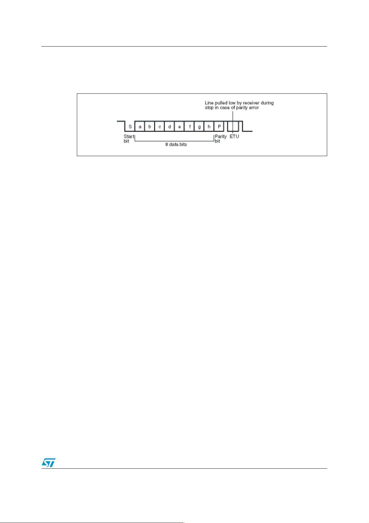
AN2646 - Application note Smartcard interface description
to the card. The length of an ETU is a bit time. The UART1 transmitter output and receiver
input are internally connected through the Rx_SW line. For the transmission of data from the
STM8S20x to the smartcard, the UART1 must be set up in smartcard mode.
Figure 1. ISO 7816-3 asynchronous protocol
1.4 Smartcard clock generator
The smartcard clock generator provides a clock signal to the connected smartcard. The
smartcard uses this clock to derive the baud rate clock for the serial I/O between the
smartcard and another UART1. The clock is also used for the CPU in the card, if present.
Operation of the smartcard interface requires that the clock rate to the card is adjusted while
the CPU in the card is running code so that the baud rate can be changed or the
performance of the card can be increased. The protocols that govern the negotiation of
these clock rates and the altering of the clock rate are detailed in the ISO 7816-3 standard.
The clock is used as the CPU clock for the smartcard, therefore updates to the
microcontroller clock rate must be synchronized to the smartcard clock, that is the clock high
or low pulse widths must not be shorter than either the old or new programmed value.
5/43
Page 6
Smartcard reader hardware connection AN2646 - Application note
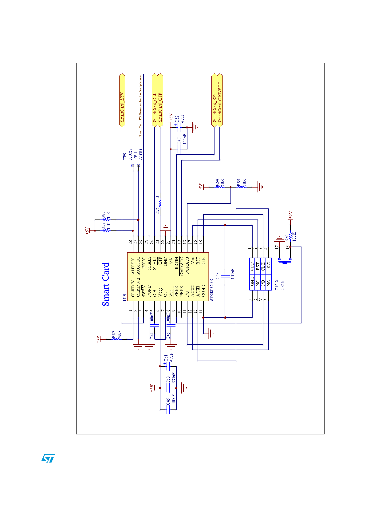
2 Smartcard reader hardware connection
To interface to the smartcard, the ST8024 device was used. The ST8024 is a complete lowcost, analog interface for asynchronous 3 V and 5 V smartcards. It is placed between the
smartcard and the STM8S20x with few external components to perform all supply protection
and control functions.
The M74HC4052 multiplexer/demultiplexer is configured by software to allow the
UART1_TX to the Smartcard_IO
Table 2. STM8S20x and smartcard connection
STM8S20x pins Smartcard pins Function
UART1_CK: PA6 C3: CLK Smartcard clock: output push-pull
UART1_TX: PA5 C7: IO IO serial data: output open drain
PG5 C2: RST Reset to card: output push-pull
PG7 C1: V
PE0 OFF Smartcard detect: input floating
PG4 3/5V 3 V or 5 V: output push-pull
CC
Supply voltage: output push-pull
6/43
Page 7
AN2646 - Application note Smartcard reader hardware connection
Figure 2. Smartcard interface hardware connection
7/43
Page 8
ISO 7816 – protocol overview AN2646 - Application note
3 ISO 7816 – protocol overview
3.1 Introduction
"ISO 7816: Identification cards -- Integrated circuit(s) cards with contacts" provides the basis
to transition the relatively simple identification card from a token that can be compromised
through forgery, theft, or loss into a tamper-resistant and "intelligent" integrated circuit card
(ICC), more popularly known as a smartcard. ISO 7816 includes at least six approved parts
and has several additional parts under review:
● Part 1: Physical characteristics
● Part 2: Dimensions and location of the contacts
● Part 3: Electrical interface and transmission protocols
● Part 3: Amendment 2-Revision of protocol type selection
● Part 4: Organization, security and commands for interchange
● Part 5: Registration of application providers
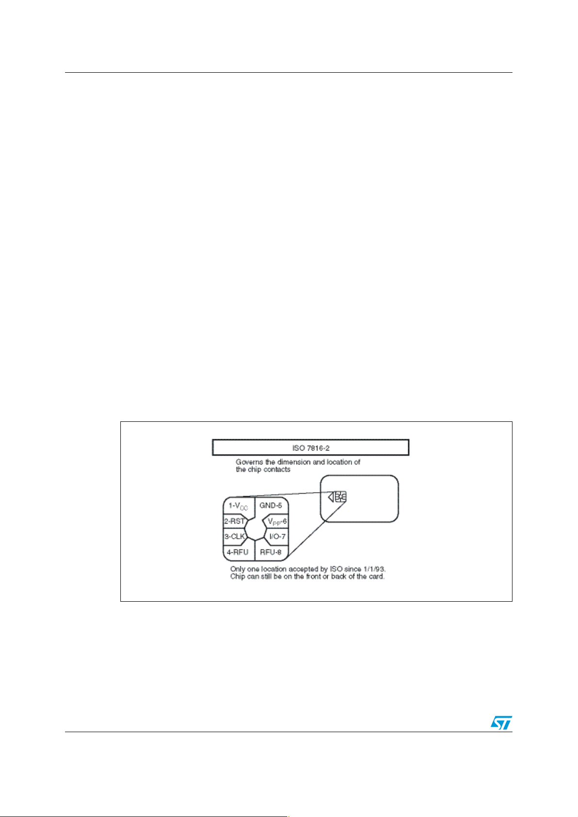
3.2 ISO 7816-2 – pin location
ISO 7816-2 specifies an ICC with eight electrical contacts present in a standardized position
on the front face of the card. These are referred to as C1 through C8. Some of these
contacts are electrically connected to the microprocessor chip embedded within the card;
some are not, having been defined to allow for enhancements but unused at the present
time. Figure 3 shows the contact positions.
Figure 3. Contact definitions for smartcards
8/43
Page 9

AN2646 - Application note ISO 7816 – protocol overview
Table 3. Pin assignment
Pins Functions
C1 V
= 5 V or 3.3 V
CC
C2 Reset
C3 Clock
C4 RFU
C5 GND
C6 V
PP
C7 I/O
C8 RFU
9/43
Page 10
ISO 7816-3 – electronic signal and transmission protocol AN2646 - Application note
4 ISO 7816-3 – electronic signal and transmission
protocol
ISO 7816-3 begins to delve into the specification of the "intelligent" aspects of the
smartcard. This standard describes the relationship between the smartcard and the reader
as one of "slave" (the smartcard) and "master" (the reader). Communications are
established by the reader signaling to the smartcard through the contacts noted previously
and are continued by the smartcard responding accordingly.
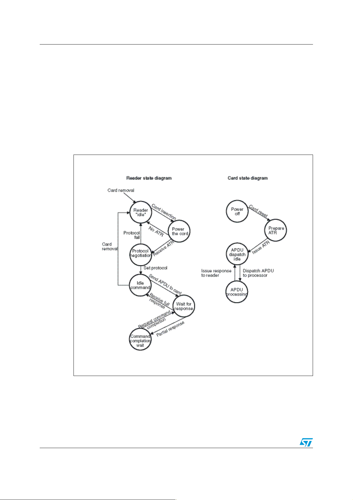
Communication between the card and reader proceed according to various state transitions
illustrated in Figure 4.
Figure 4. Reader and card FSM
The communication channel is single-threaded; once the reader sends a command to the
smartcard, it blocks until a response is received.
10/43
Page 11
AN2646 - Application note ISO 7816-3 – electronic signal and transmission protocol
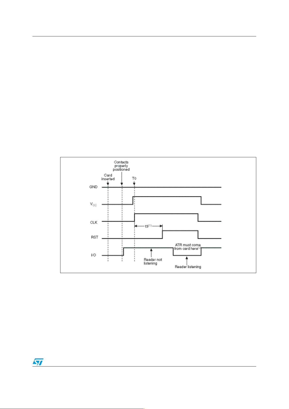
4.1 Card power-up and reset
When a card is inserted into a reader, no power is applied to any of the contacts. The chip
on the card could be seriously damaged by applying power to the wrong contacts, and this
situation could easily occur if a card were inserted across powered contact points. The
contacts remain unpowered until an edge detector determines that the card is properly
aligned with the contact points to within some acceptable (for the reader) mechanical
tolerance.
When the reader detects that the card is properly inserted, power is applied to the card.
First, the contacts are brought to a coherent idle state, as shown in Tab le 3 . A reset signal is
then sent to the card via the RST contact line. The idle state occurs when the power (V
contact is brought up to a normal, stable operating voltage of 5 V. An initial power setting of
5 V is always applied first, even though some microprocessor chips being introduced
operate at 3 V when in an I/O state. The I/O contact is set to a reception mode on the reader
side and a stable clock (CLK) is applied. The reset line is in a low state. It must remain in a
low state for at least 40 000 CLK cycles before a valid reset sequence can be started by the
reader, raising the reset line to a high state.
Figure 5. Answer to reset
CC
)
1. t3 = 40 000 clock cycles.
2. ATR must be issued by card between 400 clock cycles and 40 000 clock cycles after RST goes high.
11/43
Page 12

ISO 7816-3 – electronic signal and transmission protocol AN2646 - Application note
4.2 Data transfer
Data transfer between the reader and the card occurs through the concerted action of two of
the contact lines: CLK and I/O. The I/O line conveys a single bit of information per unit of
time as defined by the CLK depending on its voltage relative to GND. A 1 bit can be
conveyed either through a +5 V value or through a 0 V value. The actual convention used is
determined by the card and is conveyed to the reader through the "initial character" of the
ATR, which is referenced as TS. To transfer 1 byte of information, 10 bits are actually moved
across the I/O line; the first is always a "start bit" and the last is always a parity bit used to
convey even parity. Considering that the I/O line can be (in one bit period) either in a high
(H) state or a low (L) state, the TS character of the form HLHHLLLLLLH signals that the card
wants to use the "inverse convention," meaning that H corresponds to a 0 and L
corresponds to a 1. A TS character of the form HLHHLHHHLLH signals that the card wants
to use the "direct convention," meaning that H corresponds to a 1 and L corresponds to a 0.
The direct convention and the inverse convention also control the bit ordering with each byte
transferred between the card and the reader. In the direct convention, the first bit following
the start bit is the low-order bit of the byte. Successively higher-order bits follow in
sequence. In the inverse convention, the first bit following the start bit is the high-order bit of
the byte. Successively lower-order bits follow in sequence. Parity for each byte transferred
should be even; this means that the total number of 1 bits in the byte, including the parity bit,
must be an even number.
The I/O line comprises a half-duplex channel; that is, either the card or the reader can
transmit data over the same channel, but they both cannot be transmitting at the same time.
So as part of the power-up sequence, both the reader and the card enter a receive state in
which they are listening to the I/O line. With the start of the reset operation, the reader
remains in the receive state while the card must enter a send state in order to send the ATR
back to the reader. From this point on, the two ends of the channel alternate between send
states and receive states. With a half-duplex channel, there is no reliable way for either end
to asynchronously change a state from send to receive or from receive to send. Rather, if
this is desired, that end must go into a receive state and allow a timeout of the operation in
progress; then a reader end will always try to re-establish a known sequence by re-entering
a send state. The CLK and I/O lines can support a wide variety of data transmission speeds.
The specific speed is defined by the card and is conveyed back to the reader through an
optional character in the ATR. The transmission speed is set through the establishment of
one bit time on the I/O line, which means that an interval is established at which the I/O line
may be sampled in order to read a bit and then each successive bit. This time is defined as
an elementary time unit (ETU) and is established through a linear relationship between
several factors. Note that the TS character is returned before any definition of the ETU can
be made. This is possible because the ETU during the ATR sequence is always specified to
be ETU0=372/(CLK frequency) where the CLK frequency is always between 1 MHz and 5
MHz; in fact, the frequency is almost always selected such that the initial data transfer rate is
9,600 bits per second.
This initial etu is used during answer to reset and is replaced by the work etu during
subsequent transmission. F is the clock rate conversion factor and D is the bit rate
adjustment factor used to determine the work etu in subsequent transmissions.
For internal clock cards:
initial etu = 1/9600 s
work etu = (1/D)*(1/9600) s
12/43
Page 13

AN2646 - Application note ISO 7816-3 – electronic signal and transmission protocol
For external clock cards:
initial etu = 372/fi s
work etu = (1/D)*(F/fs) s
The minimum value of fs must be 1 MHz.
The maximum value of fs is given in Ta bl e 4 .
I and P define the active state on VPP.
● Maximum programming current: Ipp = 1 mA
● Programming voltage : Vpp = P.V
N is an extra guardtime requested by the card. Before receiving the next character, the card
requires a delay of at least (12+N) etu from the leading edge of the previous character. No
extra guardtime is used to send characters from the card to the interface device.
The default values of these parameters are:
F = 372; D = 1; I = 50; P = 5; N = 0
Integer values represent the number of global interface bytes
The global interface bytes, TA1, TB1, TC1, TB2 contain integer values FI,DI, II, PI1, N and
PI2 which either directly contain or are used to compute the values of the parameters F, D, I,
P, N presented above.
TA1 codes FI over the most significant half byte (b8 to b5) and DI over the least significant
half byte (b4 to b1).
TB1 codes II over bits b7 and b6, and PI1 over the 5 least significant bits b5 to b1. The most
significant bit b8 has a value of 0.
Note: The interface device may ignore bit b8 of TB1.
TC1 codes N over the eight bits (b8 to b1).
TB2 codes PI2 over the eight bits (b8 to b1).
Table 4. Clock rate conversion factor F
Parameter
FI 0000 0001 0010 0011 0100 0101 0110 0111 1000 1001 1010 1011 1100 1101 1110 1111
F
Freq
max
Val ues
372 558 774 1116 1488 1860 RFU RFU 512 768 1024 1536 2048 RFU RFU
Internal clk
- 5 6 8 12 16 20 - - 5 7.5 10 15 20 - -
RFU : Reserved for Future Use
13/43
Page 14

ISO 7816-3 – electronic signal and transmission protocol AN2646 - Application note
Table 5. Bit rate adjustment factor D
Values
Parameter
DI 0000 0001 0010 0011 0100 0101 0110 0111 1000 1001 1010 1011 1100 1101 1110 1111
D RFU 1 2 4 8 16 RFU RFU RFU RFU 1/2 1/4 1/8 1/16 1/32 RFU
RFU : Reserved for Future Use
14/43
Page 15
AN2646 - Application note ISO 7816-3 – electronic signal and transmission protocol
Programming voltage factor P
PI1 from 5 to 25 gives the value of P in volts. PI1=0 indicates that VPP is connected in the
card which generates an internal programming voltage from VCC. Other values of PI1 are
reserved for future use.
When PI2 is present, the indication of PI1 should be ignored. PI2 from 50 to 250 gives the
value of P in 0.1 V units. Other values of PI2 are reserved for future use.
Table 6. Maximum programming current factor I
Parameter Values
II 00 01 10 11
I 25 50 100 RFU
RFU : Reserved for Future Use
Extra guardtime N
N codes the extra guard time directly, from 0 to 254 etu. N=255 indicates that the minimum
delay between the start edges of two consecutive characters is reduced to 11 etu.
15/43
Page 16

ISO 7816-3 – electronic signal and transmission protocol AN2646 - Application note
4.3 Answer to reset (ATR)
Once an RST signal is sent from the reader to the card, the card must respond with the first
character of the ATR within 40 000 CLK cycles. The card might not respond with an ATR for
a number of reasons, the most prevalent being that the card is inserted incorrectly into the
reader (probably upside down). In some instances, the card may not be functioning because
it has been damaged or broken. Whatever the case, if the ATR is not returned within the
prescribed time, the reader should begin a sequence to power down the card. During this
sequence, the reader sets the RST, CLK, and I/O lines low and drops voltage on the V
line to nominal 0 (that is, less than 0.4 V).
The ATR is a string of characters returned from the card to the reader following the
successful completion of the power-up sequence. As defined in ISO/IEC 7816-3, the ATR
consists of 33 or fewer characters comprising the following elements:
● TS - a mandatory initial character
● T0 - a mandatory format character
● TAi TBi TCi TDi - optional interface characters
● T1, T2,TK - optional historical characters
● TCK - a conditional check character
The historical characters can be defined at the discretion of the card manufacturer or the
card issuer. These characters are typically used to convey some type of designation of the
type, model, and use of this specific card. When used in this way, the historical characters
provide a mechanism through which systems can automatically detect the use of an
inserted card (within that system) and can initiate other actions (or software) accordingly.
The check character provides a mechanism through which the integrity of the ATR can be
measured; that is, whether a transmission error has occurred in sending the characters from
the card to the reader.
CC
The structure of the ATR is illustrated in Tab le 7 . As discussed previously, the initial TS
character is used to establish the bit-signaling and bit-ordering conventions between the
reader and the card. The T0 character is used to signal the presence or absence of
subsequent interface characters or historical characters. The interface characters are used
to tailor the characteristics of the I/O channel, including the specific protocol used by the
card and reader during subsequent exchange of commands (from the reader to the card)
and responses (from the card to the reader). The historical characters, if present, are used
to convey card-manufacturer-specific information from the card to the read, and hence to the
application system being served by the reader. There is really no established standard for
the information presented in the historical bits.
16/43
Page 17

AN2646 - Application note ISO 7816-3 – electronic signal and transmission protocol
The total length of the ATR sequence is limited to 33 bytes and must adhere to the following
format:
Table 7. Answer-to-reset structure
Character ID Definition
Initial character section TS Mandatory initial character
Format character section T0 Indicator for presence of interface characters
TA1 Global, codes F1 and D1
TB1 Global, codes 11 and Pl1
TC1 Global, code N
TD1 Codes Y2 and T
TA 2 S pe c i fi c
Interface character section
TB2 Global, code Pl2
TC2 Specific
TD2 Codes Y3 and T
TA3 TAi, TBi and TCi are specific
..TDi Codes Yi+1 and T
T1 Card specific information
Historical character section ...TKi (Maximum of 15 characters)
Check character section TCK Optional check character
17/43
Page 18

ISO 7816-4 – smartcard commands AN2646 - Application note
5 ISO 7816-4 – smartcard commands
The previous chapter discussed the answer-to-reset (ATR) mechanism, which establishes a
basic communication channel between the smartcard and the reader. This channel is a halfduplex physical channel. This chapter investigates the use of more complex protocols on top
of this physical channel.
A link-level communication protocol resides directly on top of the physical channel, providing
error-free communication between the reader and the smartcard. Once this link-level
protocol is established, application-level protocols can be defined. ISO 7816-4 defines two
such application-level protocols:
● File system API providing a set of functions to manipulate files (for example read, write,
select, etc.).
● Security service API allowing the smartcard and the reader to mutually authenticate
themselves and also to encrypt data to be exchanged between the card and the reader.
ISO 7816-4 defines a protocol message structure to support the application protocol APIs.
This message structure consists of application protocol data units (APDUs) which are
exchanged between the reader application and the smartcard application by the link-level
protocol. This chapter will provide an overview of the file access and security APIs.
5.1 T0 protocol
The T0 protocol is a byte-oriented protocol where a character is transmitted across the
channel between the reader and the card. In addition, error handling is performed on each
byte by looking at the parity bit. If the actual parity bit does not correspond to the parity of
the transmitted data, then an error must have occurred. In the T0 protocol, the receiving side
signals that it requires the byte to be retransmitted in the case of detecting a parity error.
This is done by holding the I/O line low (normally the I/O line is set high preceding the
transfer of a byte). When the transmitting side detects this, it resends the byte that was not
received correctly.
The reader and the smartcard exchange data structures known as transmission protocol
data units (TPDUs). It consists of two distinct structures:
● a command that is sent from the reader to the card
● a response that is sent from the card to the reader
The command header includes the following five fields each of one byte in length:
● CLA: class designation of the command set to establish a collection of instructions
● INS: specifies a specific instruction from within the set of instructions
● P1: used to specify the addressing used by the [CLA, INS] instruction
● P2: also used to specify the addressing used by the [CLA, INS] instruction
● P3: specifies the number of data bytes transferred to or from the card as part of the
[CLA, INS] instruction execution.
Each value of CLA defines an application-specific set of instructions. Table 8. below lists
values for some sets of instructions.
18/43
Page 19

AN2646 - Application note ISO 7816-4 – smartcard commands
Table 8. CLA instruction set definitions
CLA byte Instruction set
0x ISO 7816-4 instructions (files and security)
10 to 7F Reserved for future use
8x or 9x ISO 7816-4 instructions
Ax Application/vendor specific instructions
B0 to CF ISO 7816-4 instructions
D0 to FE Application/vendor specific instructions
FF Reserved for protocol type selection
The INS byte is used to identify a specific instruction within a class of instructions identified
by the value of CLA.Tab le 9. lists the instructions in the ISO 7816-4 standard used to access
file system and security functions.
Table 9. ISO 7816-4 INS codes
INS value Command name INS value Command name
0E Erase Binary C0 Get Response
20 Verify C2 Envelope
70 Manage Channel CA Get Data
82 External Authenticate D0 Write Binary
84 Get Challenge D2 Write Record
88 Internal Authenticate D6 Update Binary
A4 Select File DA Put Data
B0 Read Binary DC Update Record
B2 Read Record(s) E2 Append Record
The parameters P1 and P2 are defined at the link level but are actually dependent on the
specific instruction (application level). They provide control or addressing parameters for the
various application-specific instructions. For example, in the Select File instruction, P1 is
used to indicate how the file will be referred to (by identifier, name, path etc.) and P2 offers
further refinement as to which file is to be selected. P3 defines the number of bytes to be
transmitted during the execution of the INS specified instruction. The convention used to
indicate movement of data is card-centric that is, outgoing refers to data moving from the
card to the reader and incoming refers to data moving from the reader to the card.
For each command TDPU sent from the reader, a response TPDU is sent by the card. The
response includes three mandatory fields and one optional field (all one byte in length):
● ACK: indicates that the card has received the [CLA, INS] command
● NULL: used for flow control on the I/O channel by the card. It signals (to the reader) that
the card is still processing the command and so the reader must wait before sending
another command
● SW1: status response of the current command
● SW2: (optional) also conveys a status response to the reader
19/43
Page 20

ISO 7816-4 – smartcard commands AN2646 - Application note
The ACK byte is a repeat of the INS byte from the command TPDU. If the response does not
reach the reader within a specified time, the reader may initiate an RST sequence to restart
the protocol between the reader and the card. This can be prevented if the reader receives
at least one NULL byte from the card. SW1 informs the reader of the result of the requested
instruction. The values allowed for SW1 are defined as part of the application protocol.
Some instructions require the card to send data to the reader. In this case SW2 is returned
to the reader, triggering the reader to execute a GetResponse command. The card will then
return the data bytes generated by the execution of the previous command.
5.2 Application-level protocols
The ISO 7816-4 standard addresses two areas of functionality for application software:
● File system: a set of functions is provided in the form of an API. By using this API
application software on the reader side can access files in the file system.
● Security functions: these can be used to limit access to application software or to files
on the card.
The T0 protocol is used to support application-level protocols between the smartcard
application and the reader application. These application protocols exchange data
structures called application protocol data units (APDUs). The following diagram illustrates
this architecture:
Figure 6. Application communication architecture
The APDU structure defined by ISO 7816-4 is very similar to the TPDU structure used in the
T0 protocol. In fact, when an APDU is transported by the T0 protocol, the elements of the
APDU directly overlay the elements of the TPDU.
20/43
Page 21

AN2646 - Application note ISO 7816-4 – smartcard commands
5.2.1 The ISO 7816-4 APDU
There are two types of messages used to support the ISO 7816-4 application protocols: the
command APDU (sent from the reader to the card) and the response APDU (sent from the
card to the reader).
Figure 7. Command APDU structure
The command APDU consists of a header and a body (this can be seen in the diagram
above). The header includes CLA, INS, P1 and P2 fields. As in the T0 protocol, CLA and
INS specify an application class and instruction. P1 and P2 are used to qualify specific
instructions and are given specific definitions by each [CLA, INS] instruction. The body of
the APDU can vary in size and is used to transmit data to the card's APDU processor as
part of a command or to convey a response from the card to the reader. The Lc field
specifies the number of bytes to be transmitted to the card as part of the instruction, that is,
the length of the data field. The data field contains information that must be sent to the card
to allow its APDU processor to execute the command specified in the APDU. The Le field
specifies the number of bytes that will be returned to the reader in the response APDU.
The body of the APDU can take on four different forms:
● Case 1: No data is transferred to or from the card, so the APDU only contains the
header.
● Case 2: No data is transferred to the card, but data is returned from the card. The body
of the APDU only contains a non-null Le field.
● Case 3: Data is transferred to the card, but none is returned from it. The body of the
APDU includes the Lc and data fields.
● Case 4: Data is transferred to the card and is also returned from the card as a result of
the command. The body of the APDU includes the Lc, data and Le fields.
Figure 8. Response APDU structure
The response APDU has a much simpler structure than that of the command APDU. It
consists of a body and a trailer. The body is either null or it includes a data field - depending
on the specific command. The length of the data field is determined by the Le field in the
corresponding command APDU. The trailer consists of up to two fields of status information
called SW1 and SW2. These fields return a status code in which one byte is used to specify
21/43
Page 22

ISO 7816-4 – smartcard commands AN2646 - Application note
an error category and the other is used to specify a command-specific status or error
indication.
5.2.2 File system API
The file system is used on the non-volatile memory or EEPROM. It is defined as a simple
hierarchical structure (similar to conventional file systems). The file system may contain
three types of files (identified by a 2-byte identifier):
● Master file (MF)
● Dedicated file (DF)
● Elementary file (EF)
There is one master file found on each smartcard and it is the root of the file system. A
master file may contain dedicated files or elementary files. The file identifier reserved for the
master file is 3F00. The directory file is essentially a container (or directory) for elementary
files - a DF may contain zero or more EFs. Dedicated files partition the smartcard into an
ordered structure of elementary files. A dedicated file must be given a unique file identifier
within the dedicated file or master file that contains it - allowing for a unique path for each
file. A dedicated file can also be referenced by name (1-16 bytes long). The naming
convention can be found in ISO 7816-5. An elementary file is a leaf node in the hierarchy
and contains the actual data. An elementary file can be identified by a 5-bit identifier within a
dedicated file. This file system hierarchy is illustrated in Figure 9.
Figure 9. Smartcard file system architecture
1. MF = master file, DF = dedicated file, EF = elementary file.
(1)
There are four types of elementary files:
● Transparent file
● Linear, fixed-length record file
● Linear, variable-length record file
● Cyclic, fixed-length record file
A transparent file is essentially a string of bytes, that is an unstructured binary file.
Consequently a byte offset from the start of the file is required when data is to be read or
written to this type of file. In addition, a command to read or write to a transparent file will
contain the length of the byte string to be read or written to the file.
Fixed- and variable-length files contain records that are identified by a sequence number. In
a fixed-length record file, all the records contain the same number of bytes. In contrast, a
22/43
Page 23

AN2646 - Application note ISO 7816-4 – smartcard commands
variable-length record file contains records that may vary in length. As a result, variablelength record files have a higher overhead in read/write access times as well as a higher
administrative overhead required by the file system.
A cyclic file allows applications to access records in a consistent and transparent manner. It
can be thought of as a ring of files. Write operations are performed on the next physical
record in the ring.
5.2.3 ISO 7816-4 functions
The few functions that are defined in ISO 7816-4 for selecting, reading and writing to files
will be briefly discussed below.
Select File
This command establishes a logical pointer to a particular file in the smartcard's file system.
This pointer is required for any file manipulation operation. Access to the smartcard's file
system is not multithreaded, however it is possible to have several file pointers defined at
any point in time. This is accomplished by the Manage Channel command, which
establishes multiple logical channels between the reader side application and the card. This
allows different files on the card to be in various states of access by the reader application at
the same time. The identification of the file can be provided in the following ways:
● file identifier (2-byte value)
● DF name (string of bytes)
● path (concatenation of file identifiers)
● short ID
Note that not all smartcards support all four naming mechanisms.
Read Binary
This command is used by the application on the reader side to retrieve a part of an EF on
the card. However, the EF must be a transparent file (not record-oriented). If the Read
Binary command is attempted on a record-oriented EF, the command will abort with an error
indicator being returned from the card.
The Read Binary command takes two parameters: an offset pointer from the start of the file
to the initial byte to be read, and the number of bytes to be read and returned to the reader.
Write Binary
This command is used to insert data into a transparent EF on the card. This command can
be used to set a series of bytes in the EF (that is set selected bits within a specified byte to a
value of1), clear a series of bytes or perform a write of a series of bytes in the EF.
Update Binary
A reader-side application can utilize this command to directly erase and store a contiguous
sequence of bytes in a transparent EF on the card. It effectively functions as a write
command that is a string of bytes provided in the command are written into the EF on the
card. The input parameters consist of an offset pointer from the start of the file as well as the
number of bytes to be written.
23/43
Page 24

ISO 7816-4 – smartcard commands AN2646 - Application note
Erase Binary
The Erase Binary command is used to clear bytes within a transparent EF on a card.
Similarly to the previous commands, the input parameters comprise an offset from the start
of the EF to the segment of bytes to be erased as well as the number of bytes to be erased.
Read Record
This command is used to read and return the contents of one or more records in an EF on a
card. Unlike the previous command, the EF for the Read Record command must be a
record-oriented file. If it is applied to a transparent EF, the command will abort and an error
will be returned to the reader.
The following may be returned from this command, depending on the input parameters:
● A specified record
● All the records from the beginning of the file to a specific record
● All the records from a specific record to the end of the file
Write Record
This command is used to write a record into a record-oriented EF. As with the Write Binary
command, this command can be used to write a record into an EF, set or clear specific bits
within a specific record in an EF.
Append Record
The Append Record command is used to add a record to the end of a linear, record-oriented
EF or to write the first record to a cyclic, record-oriented EF on a card.
Update Record
This command writes a specific record into a record-oriented EF on a card. As with the
Update Binary command, the old record is erased and the new one is written into the EF.
Get Data
This command reads and returns the contents of a data object stored within the file system
on the card. The Get Data command is card-specific as the definition of a data object varies
between different cards.
Put Data
This command (as the name suggests) puts information into a data object on the card. As
with the previous command, this is a card-specific command.
5.2.4 Security API
Each component of the file system on a smartcard has an associated list of access
properties. The access properties ensure that only authorized parties are allowed to access
the particular component of the file system. The authentication can be simple, such as
requiring the reader to provide a predefined personal identification number (PIN).
Alternatively, it may be more complicated, such as requiring the reader to prove that it
possesses some shared secret with the card (for example a key) by encrypting or decrypting
a string of bytes provided by the card.
A few of the functions provided by the security API are briefly discussed below.
24/43
Page 25

AN2646 - Application note ISO 7816-4 – smartcard commands
Verify
This command is sent by the application on the reader side to the security system on the
card. Its purpose is to convince the card that the reader knows a password maintained by
the card in order to restrict access to sensitive information stored on the card. The
password-type information may be associated with a specific file or to some or all of the file
hierarchy. If the Verify command fails i.e. the reader provides an incorrect password, an error
is returned to the reader.
Internal Authenticate
This command allows the card to authenticate itself to the reader by proving that it
possesses a secret key shared with the reader. The reader application software first
generates a random number and encrypts it with some algorithm known to both card and
reader. This constitutes a challenge to the card. The card then decrypts this challenge with
the secret key (that is stored on the card) and sends the resulting data back to the reader. If
the data received by the reader matches the random number that it generated then the
reader application software is assured of the identity of the card.
External Authenticate
This command is used in conjunction with the Get Challenge command to enable the reader
application software to authenticate itself to the card. The reader receives challenge data (a
random number) from the card and encrypts it with a secret key. This is then sent to the card
using the External Authenticate command. The card decrypts the data and compares it to
the random number that it generated in the previous Get Challenge command. If there is a
match, then the card is assured of the identity of the reader application.
Get Challenge
This command is sent by the reader to the card. Its purpose is to provide the reader
application with a random number generated by the smartcard. As previously described, this
number is used in the External Authenticate command.
Manage Channel
The Manage Channel command is used by the reader application to open and close the
logical communication channels between it and the card. Initially the card opens a basic
communication channel by establishing an application-level protocol with the reader
application through the completion of an ATR sequence. This channel is then used to open
or close additional logical channels through the Manage Channel command.
Envelope
This command supports the use of secure messaging using the T0 protocol. It enables an
APDU to be encrypted and then incorporated into the Envelope command's data section (of
its APDU). The APDU processor on the card can then extract and execute the command.
Get Response
As with the previous command, the Get Response command allows the use of the T0
protocol for transferring APDUs. The Case 4 type of APDU cannot be supported by the T0
protocol i.e. it is not possible to send a block of data to the card and then receive a block of
data in return. So when using the T0 protocol, the initial command results in a response
which indicates that more data is waiting to be sent by the card. The Get Response
command is then used to retrieve this data.
25/43
Page 26

Smartcard interface library: description AN2646 - Application note
6 Smartcard interface library: description
The user may access a smartcard using directly the application layer. It allows to
send/receive ADPU commands to/from the smartcard using the following user interface:
6.1 File organization
Ta bl e 1 0 presents the smartcard library modules:
Table 10. File library description
File Description
– Smartcard definitions, types definitions and function prototypes
smartcard.h, smartcard.c
6.2 Smartcard interface library functions
– T0 protocol management
– Physical layer
Ta bl e 1 3 lists the various functions of the smartcard library.
Table 11. Smartcard library functions
Function name Description
SC_Handler
SC_PowerCmd Enables or disables the power to the smartcard.
SC_Reset Sets or clears the smartcard reset pin.
SC_ParityErrorHandler
SC_PTSConfig Configures the IO speed (BaudRate) communication.
Handles all smartcard states and serves to send and receive all
communication data between smartcard and reader.
Resends the byte that failed to be received (by the smartcard)
correctly.
26/43
Page 27

AN2646 - Application note Smartcard interface library: description
6.2.1 SC_Handler function
Function name SC_Handler
Function prototype
Behavior description
Input parameter1
Input parameter2
Input parameter3
void SC_Handler(SC_State *SCState, SC_ADPU_Commands *SC_ADPU,
SC_ADPU_Responce *SC_Response)
Handles all smartcard states and serves to send and receive all
communication data between smartcard and reader.
SCState: pointer to an SC_State enumeration that will contain the
smartcard state.
SC_ADPU: pointer to an SC_ADPU_Commands structure that will be
initialized.
SC_Response: pointer to a SC_ADPU_Responce structure which will be
initialized.
Output parameter None
Return parameter None
Required preconditions None
Called functions None
SCState
SCState informs the user about the smartcard state and allows the user to power off the
smartcard. It can take one of the values defined in Ta bl e 1 2 below.
Table 12. SCState
SCState Meaning
SC_POWER_OFF
SC_POWER_ON
SC_RESET_LOW
SC_RESET_HIGH
SC_ACTIVE
SC_ACTIVE_ON_T0
No power is provided to the smartcard (V
= 0); the STM8S20x smartcard
CC
interface is disabled. No clock is provided to the smartcard.
The smartcard peripheral is enabled and initialized; no power is provided to
the smartcard; no clock is provided to the smartcard.
In this state, the RST smartcard pin (pin 2) is driven low (RST = 0). V
CC
=
5 V is provided to the smartcard; clock CLK is provided to the smartcard.
Answer to reset (ATR) procedure begins. The reader waits for an ATR frame
from the smartcard.
If no answer is received, the reader forces the reset pin RST high (RST = 1)
and holds it high until it receives an answer to reset.
If an answer to reset is received, the reader goes in active state and
decodes the ATR frame. It returns information about the used protocol.
If the used protocol is T0, the reader goes in SC_ACTIVE_ON_T0 state and
commands can then be sent to the smartcard.
27/43
Page 28

Smartcard interface library: description AN2646 - Application note
Figure 10. State machine for smartcard operation
SC_ADPU_Commands
The SC_APDU_Commands structure is defined in the smartcard.h file:
typedef struct
{
SC_Header Header;
SC_Body Body;
} SC_ADPU_Commands;
●
Header
Specifies the APDU command header. It is of the SC_Header type, which is defined in
the smartcard.h file:
typedef struct
{
u8 CLA; /* Command class */
u8 INS; /* Operation code */
u8 P1; /* Selection Mode */
u8 P2; /* Selection Option */
} SC_Header;
●
CLA
Specifies the class designation of the command set to establish a collection of
instructions.
● INS
Specifies a specific instruction from within the set of instructions.
● P1
Specifies the addressing used by the [CLA, INS] instruction.
● P2
Specifies the addressing used by the [CLA, INS] instruction.
● Body
Specifies the APDU command body. It is of the SC_Body type, which is defined in the
smartcard.h file:
28/43
Page 29

AN2646 - Application note Smartcard interface library: description
typedef struct
{
u8 LC; /* Data field length */
u8 Data[LCmax]; /* Command parameters */
u8 LE; /* Expected length of data to be returned */
} SC_Body;
●
LC
Specifies the number of data bytes transferred to the card as part of the [CLA, INS]
instruction execution.
● Data
Specifies the pointer to the data buffer transferred to the card.
● LE
Specifies the number of data bytes transferred from the card as part of the [CLA, INS]
instruction execution.
● SC_Response
Specifies the APDU command response. It is of SC_ADPU_Response type, defined in
the smartcard.h file:
typedef struct
{
u8 Data[LCmax]; /* Data returned from the card */
u8 SW1; /* Command Processing status */
u8 SW2; /* Command Processing qualification */
} SC_ADPU_Responce;
●
Data
Specifies the pointer to the data buffer which will contain the returned card data.
● SW1
Specifies the first status code byte. This byte stores the error category.
● SW2
Specifies the second status code byte. This byte stores a command-specific status or
error indication.
Example:
/* Select the Master Root MF */
SC_ADPU.Header.CLA = SC_CLA;
SC_ADPU.Header.INS = SC_SELECT_FILE;
SC_ADPU.Header.P1 = 0x00;
SC_ADPU.Header.P2 = 0x00;
SC_ADPU.Body.LC = 0x02;
for(i = 0; i < SC_ADPU.Body.LC; i++)
{
SC_ADPU.Body.Data[i] = MasterRoot[i];
}
while(i < LCmax)
{
SC_ADPU.Body.Data[i++] = 0;
}
SC_ADPU.Body.LE = 0;
SC_Handler(&SCState, &SC_ADPU, &SC_Responce);
29/43
Page 30

Smartcard interface library: description AN2646 - Application note
6.2.2 SC_PowerCmd
Function name SC_PowerCmd
Function prototype
Behavior description Enables or disables the power to the smartcard.
Input parameter
Output parameter None
Return parameter None
Required preconditions None
Called functions None
Example:
/* Power ON the card */
SC_PowerCmd(ENABLE);
6.2.3 SC_Reset
Function name SC_Reset
Function prototype
Behavior description Sets or clears the smartcard reset pin.
Input parameter
Output parameter None
Return parameter None
void SC_PowerCmd(FunctionalState NewState);
NewState: new state of the smartcard power supply. This parameter
can be: ENABLE or DISABLE.
void SC_Reset(BitAction ResetState);
ResetState: this parameter specifies the state of the smartcard reset pin.
BitVal must be one of the BitAction enum values:
Bit_RESET: to clear the port pin.
Bit_SET: to set the port pin.
Required preconditions None
Called functions None
Example:
/* Set the smartcard reset pin */
SC_Reset(Bit_SET);
30/43
Page 31

AN2646 - Application note Smartcard interface library: description
6.2.4 SC_ParityErrorHandler
Function name SC_ParityErrorHandler
Function prototype
Behavior description Resends the byte that failed to be received correctly (by the smartcard)
Input parameter None
Output parameter None
Return parameter None
Required preconditions None
Called functions None
Example:
/* Resend the byte to the smartcard */
SC_ParityErrorHandler();
6.2.5 SC_PTSConfig
Function name SC_PTSConfig
Function prototype
Behavior description Configures the IO speed (BaudRate) communication.
Input parameter None
Output parameter None
void SC_ParityErrorHandler(void);
void SC_PTSConfig(void);
Return parameter None
Required preconditions Must be called just after the ATR sequence.
Called functions None
Example:
/* Configures the baudrate according to the card TA1 value */
SC_PTSConfig();
31/43
Page 32

Smartcard interface library: description AN2646 - Application note
6.3 How to send APDU commands to the smartcard
A detailed description on how to use the SC_Handler( ) function to send the ADPU
command to the smartcard and retrieve the card response is described below. The user has
to update the SC_CLA and the smartcard instruction values according to the smartcard
specifications.
6.3.1 SC_GET_A2R
SC_ADPU.Header.CLA = 0x00;
SC_ADPU.Header.INS = SC_GET_A2R;
SC_ADPU.Header.P1 = 0x00;
SC_ADPU.Header.P2 = 0x00;
SC_ADPU.Body.LC = 0x00;
while(SCState != SC_ACTIVE_ON_T0)
{
SC_Handler(&SCState, &SC_ADPU, &SC_Responce);
}
●
SCState: It stores the current smartcard state.
● SC_ATR_Table: Pointer to an array (filled in by the SC_Handler function) that
contains the smartcard ATR frame.
6.3.2 SELECT_FILE
SC_ADPU.Header.CLA = SC_CLA;
SC_ADPU.Header.INS = SC_SELECT_FILE;
SC_ADPU.Header.P1 = 0x00;
SC_ADPU.Header.P2 = 0x00;
SC_ADPU.Body.LC = 0x02;
for(i = 0; i < SC_ADPU.Body.LC; i++)
{
SC_ADPU.Body.Data[i] = FileName[i];
}
while(i < LCmax)
{
SC_ADPU.Body.Data[i++] = 0;
}
SC_ADPU.Body.LE = 0;
SC_Handler(&SCState, &SC_ADPU, &SC_Responce);
●
FileName: It contains the 16 bit file identifier.
● SCState: It stores the current smartcard state.
● SC_Response->SW1 and SC_Response->SW2: they return the smartcard response
to the SC_SELECT_FILE command.
6.3.3 SC_GET_RESPONSE
SC_ADPU.Header.CLA = SC_CLA;
SC_ADPU.Header.INS = SC_GETRESPONSE;
SC_ADPU.Header.P1 = 0x00;
SC_ADPU.Header.P2 = 0x00;
SC_ADPU.Body.LC = 0x00;
i = 0;
while(i < LCmax)
{
32/43
Page 33

AN2646 - Application note Smartcard interface library: description
SC_ADPU.Body.Data[i++] = 0;
}
SC_ADPU.Body.LE = SC_Responce.SW2;
SC_Handler(&SCState, &SC_ADPU, &SC_Responce);
●
SCState: It stores the current smartcard state.
● SC_Response->SW1 and SC_Response->SW2: they return the smartcard response
to the SC_GET_RESPONSE command.
● SC_Response->Data: It returns the smartcard data response to the
SC_GET_RESPONSE command.
6.3.4 SC_READ_BINARY
SC_ADPU.Header.CLA = SC_CLA;
SC_ADPU.Header.INS = SC_READ_BINARY;
SC_ADPU.Header.P1 = OFFSET_MSB;
SC_ADPU.Header.P2 = OFFSET_LSB;
SC_ADPU.Body.LC = 0x00;
while(i < LCmax)
{
SC_ADPU.Body.Data[i++] = 0;
}
SC_ADPU.Body.LE = LENGTH;
SC_Handler(&SCState, &SC_ADPU, &SC_Responce);
●
SCState: It stores the current smartcard state.
● OFFSET_MSB: Most significant byte of offset for reading data.
● OFFSET_LSB: Least significant byte of offset for reading data.
● LENGTH: It contains size (in byte) of the area to read (valid only for the elementary
file).
● SC_Response->Data: It returns the smartcard data to read.
● SC_Response->SW1 and SC_Response->SW2: they return the smartcard response
to the SC_READ_BINARY command.
6.3.5 SC_CREATE_FILE
SC_ADPU.Header.CLA = SC_CLA;
SC_ADPU.Header.INS = SC_CREATE_FILE;
SC_ADPU.Header.P1 = 0x00;
SC_ADPU.Header.P2 = 0x00;
SC_ADPU.Body.LC = 0x10;
for(i = 0; i < SC_ADPU.Body.LC; i++)
{
SC_ADPU.Body.Data[i] = FileParameters[i];
}
while(i < LCmax)
{
SC_ADPU.Body.Data[i++] = 0;
}
SC_ADPU.Body.LE = 0;
SC_Handler(&SCState, &SC_ADPU, &SC_Responce);
33/43
Page 34

Smartcard interface library: description AN2646 - Application note
● FileParameters: It contains the 16 bytes file parameters (File ID, FILE Access
Conditions...).
● SCState: It stores the current smartcard state.
● SC_Response->SW1 and SC_Response->SW2: they return the smartcard response
to the SC_CREATE_FILE command.
6.3.6 SC_UPDATE_BINARY
SC_ADPU.Header.CLA = SC_CLA;
SC_ADPU.Header.INS = SC_UPDATE_BINARY;
SC_ADPU.Header.P1 = OFFSET_MSB;
SC_ADPU.Header.P2 = OFFSET_LSB;
SC_ADPU.Body.LC = LENGTH;
while(i < LCmax)
{
SC_ADPU.Body.Data[i++] = 0;
}
SC_ADPU.Body.LE = 0x00;
SC_Handler(&SCState, &SC_ADPU, &SC_Responce);
●
SCState: It stores the current smartcard state.
● OFFSET_MSB: Most significant byte of offset for reading data.
● OFFSET_LSB: Least significant byte of offset for reading data.
● LENGTH: It contains the size (in byte) of the area to write (valid only for the elementary
file).
● SC_Responce->Data: It contains the smartcard data to write.
● SC_Responce->SW1 and SC_Responce->SW2: they return the smartcard response
to the SC_UPDATE_BINARY command.
6.3.7 SC_VERIFY
SC_ADPU.Header.CLA = SC_CLA;
SC_ADPU.Header.INS = SC_VERIFY;
SC_ADPU.Header.P1 = 0x00;
SC_ADPU.Header.P2 = 0x00;
SC_ADPU.Body.LC = 0x08;
for(i = 0; i < SC_ADPU.Body.LC; i++)
{
SC_ADPU.Body.Data[i] = CHV1[i];
}
while(i < LCmax)
{
SC_ADPU.Body.Data[i++] = 0;
}
SC_ADPU.Body.LE = 0;
SC_Handler(&SCState, &SC_ADPU, &SC_Responce);
●
CHV1: It contains the 8-byte CHV1 code.
● SCState: It stores the current smartcard state.
● SC_Responce->SW1 and SC_Responce->SW2: they return the smartcard response
to the SC_VERIFY command.
34/43
Page 35

AN2646 - Application note Smartcard interface library: description
6.4 Parity error management
In the T0 protocol, error handling is performed on each byte by looking at the parity bit. If the
actual parity bit does not correspond to the parity of the transmitted data, then an error must
have occurred; the receiving side signals that it requires the byte to be retransmitted in the
case of detecting a parity error. This is done by holding the I/O line low (normally the I/O line
is set high preceding the transfer of a byte). When the transmitting side detects this, it
resends the byte that was not received correctly.
6.4.1 Data sent from card to reader
STM8S20x is able to detect a parity error on a received data via hardware, by pulling down
the data line during the stop bit.
6.4.2 Data sent from reader to card
The smartcard pulls down the I/O line to signal that a parity error occurred, the STM8S20x is
able to detect a frame error via software. The smartcard library uses the
SC_ParityErrorHandler() function to check whether a parity error has occurred and,
to manage the error if any.
After a byte is sent from the microcontroller to the card, the smartcard captures the data
sent on the I/O line. If a parity error is detected from the card, the I/O line is pulled down
during the stop bits. A frame error event occurs and the SC_ParityErrorHandler() function
resends the last data.
35/43
Page 36

Smartcard interface example AN2646 - Application note
7 Smartcard interface example
An example is provided in conjunction with the smartcard library in order to help the user
develop its custom application.
The example provides simple operations with an ISO 7816-3/4-compatible GSM11.11
smartcard, such as file system exploration, pin1 enable/disable, read/write operation on files
and pin verify on protected files.
This example was developed to run on the STM8/128-EVAL (evaluation board) that provides
all needed hardware to interface a smartcard.
7.1 Firmware package description
The STM8S20x smartcard application note firmware package contains both the smartcard
library and the example described in this section.
The firmware package contains the following subfolders:
7.1.1 FWLib folder
The FWlib folder contains all the subdirectories and files that make up the core of the
STM8S20XFWLib (firmware library):
● inc subfolder contains the firmware library header files
● src subfolder contains the firmware library source files
7.1.2 Smartcard_AN folder
The Smartcard_AN folder contains all the subdirectories and files that make up the core of
the smartcard Interface application example:
● include subfolder contains the example header files
● source subfolder contains the example source files
● project subfolder contains the project that compile the example files:
36/43
Page 37

AN2646 - Application note Smartcard interface example
Configure the Multiplexer
Smartcard detected
No
Initialization
Ye s
Power On
Power Command
Power On
Power Off
Reset card and
Decode Answer
Power Off
Disable smartcard interface
Answer received
Smartcard Active on T0 protocol
Protocol type Selection configuration
Select Master File and get Reponse
Select and read ICCID File
Select GSMDir Folder
Select the IMSI File
wait for Answer
7.2 Firmware description
Figure 11. Smartcard software example flowchart
Three directories have been defined for the GSM smartcard directory tree:
MasterRoot[3]={0x3F, 0x00};
GSMDir[3]={0x7F, 0x20};
TelecomDir[3]={0x7F, 0x10};
37/43
Page 38

Smartcard interface example AN2646 - Application note
Figure 12. Smartcard example: file system description
At the end of the example:
● The ICCID file located under the MasterRoot directory is read
● The IMSI file, under GSMDir, that has a secure access through PIN1, is read
● The PIN1 is enabled/disabled
7.2.1 Smartcard startup: answer to reset (A2R)
The first action to perform when the reader wants to access a card is the answer-to-reset
procedure. To this aim the SC_Handler is invoked as follows:
SC_ADPU.Header.CLA = 0x00;
SC_ADPU.Header.INS = SC_GET_A2R;
SC_ADPU.Header.P1 = 0x00;
SC_ADPU.Header.P2 = 0x00;
SC_ADPU.Body.LC = 0x00;
while(SCState != SC_ACTIVE_ON_T0)
{
SC_Handler(&SCState, &SC_ADPU, &SC_Responce);
}
When a card is detected, the A2R sequence is generated, received and decoded. If the
recognized protocol is the T0 protocol, the smartcard state of the reader is active
(SC_ACTIVE_ON_T0) and the smartcard is available for operations on the file system.
The procedure type selection (PTS) will be applied after the ATR using the SC_PTSConfig()
function. For the used GSM card, the PTS procedure is as follows:
PTSS = 0xFF
PTS0 = 0x10
PTS1 = 0x95
PCK = 0x7A
PTS1 = 0x95, F = 9 and D = 5, Fi = 512, Di = 16, BaudRate = 112500 baud.
7.2.2 Reading a file at a specified path
The specified reading path is assumed to be: MasterRoot/GSMDir/IMSI
To reach it, the following actions are performed:
● Select GSMDir using a SelectFile APDU command
● Select IMSI File using a SelectFile APDU command
The user has to get the file characteristics to check its access conditions. The IMSI file has a
CHV1(PIN1) read condition, so PIN1 has to be checked before reading it. The verify
command must be executed under the directory containing the file to be read, the GSMDir
must be selected in the example.
38/43
Page 39

AN2646 - Application note Smartcard interface example
CLA=0xA0: to Select class GSM11
INS=0xA4: command to Select file
P1=0x00: not used
P2=0x00: not used
LC=0x02: Data file length
If SW1=0x00 Data: Address of the file or the folder to select
SW1 or SW1 and SW2 or ACK or NULL
CLA=0xA0: to Select class GSM11
INS=0xC2: command to get response
P1=0x00: not used
P2=0x00: not used
LE=SW2 : length of data to be returned
SW1 or SW1 and SW2 or ACK or NULL
Command
Select file
Command
Get response
GSM Card
Smartcard Interface
Receive the LE bytes from the card if SW1=0x00
To get file characteristics:
● Select the file the characteristics of which are needed
● Get the data returned after issuing the SelectFile APDU command by sending a
GETRESPONSE command
The IMSI file has 9 data bytes, so to run correctly the READ_BINARY commands, the
following parameters are used:
● P1 = 0x00
● P2 = 0x00
● LE = 0x09
Figure 13. Get Response from a file at a specified path (example)
39/43
Page 40

Smartcard interface example AN2646 - Application note
7.2.3 Enabling/disabling the PIN1 (CHV1) code
At the beginning of the application, the PIN1 (CHV1) status is checked. This can be done by
a GET_RESPONSE command after a successful MasterRoot selection.
In this example, the PIN1 status is checked. If it is enabled, the PIN1 will be disabled to give
access to all files that have a secure access conditions.
To check the PIN1 status, the procedure is the following:
● Select the MasterRoot directory using a SelectFile APDU command
● Get the data returned after issuing the MasterRoot SelectFile command by sending a
GETRESPONSE command.
● Check the bit8 of the 14 received bytes: if bit8 is 0: PIN1 is enabled else the PIN1 is
disabled.
To enable or disable PIN1, the CHV1 code must be sent to the card. The CHV1 code is 8byte long.
7.2.4 Verifying the PIN1 (CHV1) code
Some files have a restricted access conditions such as IMSI, CHV1 file, CHV2. The access
conditions of these files must be met for the user to be allowed to execute the restricted
operations (read, update, change CHV1).
To verify the PIN1 (CHV1) condition, the procedure is as follows:
● Go to the directory which contain the file to be accessed
● Use the Verify APDU command by presenting the CHV1 code
● Select the file and execute the selected operation
40/43
Page 41

AN2646 - Application note Conclusion
8 Conclusion
Using the STM8S UART1’s smartcard mode that supports the ISO 7816-3/4 specification,
you can develop a smartcard-based application with reduced firmware and hardware
resources.
41/43
Page 42

Revision history AN2646 - Application note
9 Revision history
Table 13. Document revision history
Date Revision Changes
04-Mar-2008 1 Initial release.
19-Aug-2008 2 Renamed USART to UART1.
42/43
Page 43

AN2646 - Application note
Please Read Carefully:
Information in this document is provided solely in connection with ST products. STMicroelectronics NV and its subsidiaries (“ST”) reserve the
right to make changes, corrections, modifications or improvements, to this document, and the products and services described herein at any
time, without notice.
All ST products are sold pursuant to ST’s terms and conditions of sale.
Purchasers are solely responsible for the choice, selection and use of the ST products and services described herein, and ST assumes no
liability whatsoever relating to the choice, selection or use of the ST products and services described herein.
No license, express or implied, by estoppel or otherwise, to any intellectual property rights is granted under this document. If any part of this
document refers to any third party products or services it shall not be deemed a license grant by ST for the use of such third party products
or services, or any intellectual property contained therein or considered as a warranty covering the use in any manner whatsoever of such
third party products or services or any intellectual property contained therein.
UNLESS OTHERWISE SET FORTH IN ST’S TERMS AND CONDITIONS OF SALE ST DISCLAIMS ANY EXPRESS OR IMPLIED
WARRANTY WITH RESPECT TO THE USE AND/OR SALE OF ST PRODUCTS INCLUDING WITHOUT LIMITATION IMPLIED
WARRANTIES OF MERCHANTABILITY, FITNESS FOR A PARTICULAR PURPOSE (AND THEIR EQUIVALENTS UNDER THE LAWS
OF ANY JURISDICTION), OR INFRINGEMENT OF ANY PATENT, COPYRIGHT OR OTHER INTELLECTUAL PROPERTY RIGHT.
UNLESS EXPRESSLY APPROVED IN WRITING BY AN AUTHORIZED ST REPRESENTATIVE, ST PRODUCTS ARE NOT
RECOMMENDED, AUTHORIZED OR WARRANTED FOR USE IN MILITARY, AIR CRAFT, SPACE, LIFE SAVING, OR LIFE SUSTAINING
APPLICATIONS, NOR IN PRODUCTS OR SYSTEMS WHERE FAILURE OR MALFUNCTION MAY RESULT IN PERSONAL INJURY,
DEATH, OR SEVERE PROPERTY OR ENVIRONMENTAL DAMAGE. ST PRODUCTS WHICH ARE NOT SPECIFIED AS "AUTOMOTIVE
GRADE" MAY ONLY BE USED IN AUTOMOTIVE APPLICATIONS AT USER’S OWN RISK.
Resale of ST products with provisions different from the statements and/or technical features set forth in this document shall immediately void
any warranty granted by ST for the ST product or service described herein and shall not create or extend in any manner whatsoever, any
liability of ST.
ST and the ST logo are trademarks or registered trademarks of ST in various countries.
Information in this document supersedes and replaces all information previously supplied.
The ST logo is a registered trademark of STMicroelectronics. All other names are the property of their respective owners.
© 2008 STMicroelectronics - All rights reserved
STMicroelectronics group of companies
Australia - Belgium - Brazil - Canada - China - Czech Republic - Finland - France - Germany - Hong Kong - India - Israel - Italy - Japan -
Malaysia - Malta - Morocco - Singapore - Spain - Sweden - Switzerland - United Kingdom - United States of America
www.st.com
43/43
 Loading...