

Page 1
AN2644
Application note
An introduction to LLC resonant
half-bridge converter
Introduction
Although in existence for many years, only recently has the LLC resonant converter, in
particular in its half-bridge implementation, gained in the popularity it certainly deserves. In
many applications, such as flat panel TVs, 85+ ATX PCs or small form factor PCs, where the
requirements on efficiency and power density of their SMPS are getting tougher and
tougher, the LLC resonant half-bridge with its many benefits and very few drawbacks is an
excellent solution. One of the major difficulties that engineers are facing with this topology is
the lack of information concerning the way it operates. The purpose of this application note
is to provide insight into the topology and help familiarize the reader with it, therefore, the
approach is essentially descriptive.
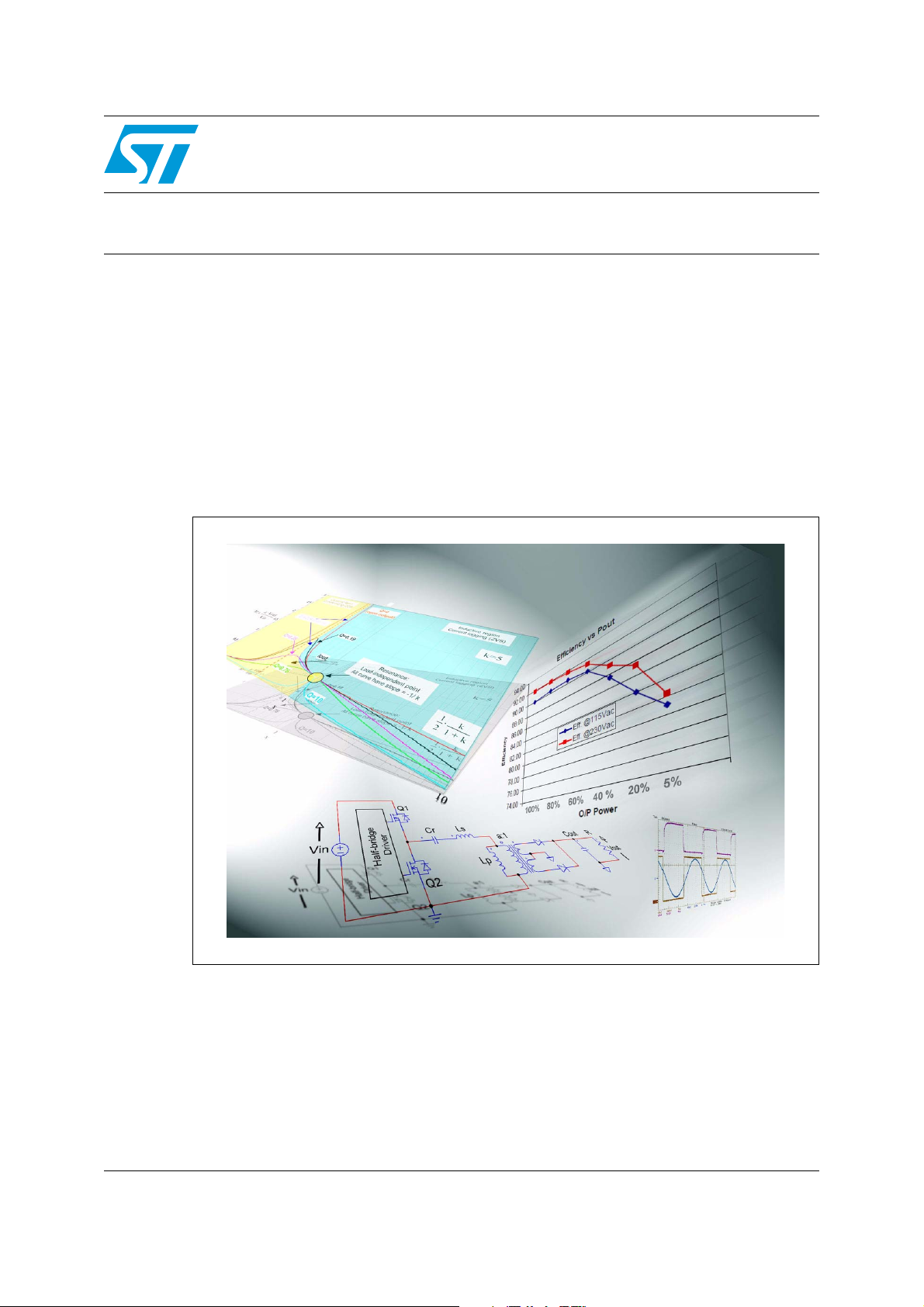
Figure 1. LLC resonant topology schematics and waveforms
September 2008 Rev 2 1/64
www.st.com
Page 2

Contents AN2644
Contents
1 Classification of resonant converters . . . . . . . . . . . . . . . . . . . . . . . . . . . 5
2 The LLC resonant half-bridge converter . . . . . . . . . . . . . . . . . . . . . . . . . 7
2.1 General overview . . . . . . . . . . . . . . . . . . . . . . . . . . . . . . . . . . . . . . . . . . . . 7
2.2 The switching mechanism . . . . . . . . . . . . . . . . . . . . . . . . . . . . . . . . . . . . 12
2.3 Fundamental operating modes . . . . . . . . . . . . . . . . . . . . . . . . . . . . . . . . . 20
2.3.1 Operation at resonance (f = fR1) . . . . . . . . . . . . . . . . . . . . . . . . . . . . . . 21
Remarks . . . . . . . . . . . . . . . . . . . . . . . . . . . . . . . . . . . . . . . . . . . . . . . . . . . . . . . .23
2.3.2 Operation above resonance (f > fR1) . . . . . . . . . . . . . . . . . . . . . . . . . . . 24
CCMA operation at heavy load. . . . . . . . . . . . . . . . . . . . . . . . . . . . . . . . . . . . . . .25
Remarks . . . . . . . . . . . . . . . . . . . . . . . . . . . . . . . . . . . . . . . . . . . . . . . . . . . . . . . .26
DCMA at medium load . . . . . . . . . . . . . . . . . . . . . . . . . . . . . . . . . . . . . . . . . . . . .28
Remarks . . . . . . . . . . . . . . . . . . . . . . . . . . . . . . . . . . . . . . . . . . . . . . . . . . . . . . . .28
DCMAB at light load . . . . . . . . . . . . . . . . . . . . . . . . . . . . . . . . . . . . . . . . . . . . . . .29
Remarks . . . . . . . . . . . . . . . . . . . . . . . . . . . . . . . . . . . . . . . . . . . . . . . . . . . . . . . .29
2.3.3 Operation below resonance (fR2 < f < fR1, R>R
DCMAB at medium-light load . . . . . . . . . . . . . . . . . . . . . . . . . . . . . . . . . . . . . . . .30
DCMB at heavy load. . . . . . . . . . . . . . . . . . . . . . . . . . . . . . . . . . . . . . . . . . . . . . .30
Remarks . . . . . . . . . . . . . . . . . . . . . . . . . . . . . . . . . . . . . . . . . . . . . . . . . . . . . . . .33
2.3.4 Capacitive-mode operation below resonance (fR2 < f < fR1, R<R
Remarks . . . . . . . . . . . . . . . . . . . . . . . . . . . . . . . . . . . . . . . . . . . . . . . . . . . . . . . .36
) . . . . . . . . . . . . . . . . 30
crit
) . . . 34
crit
2.4 No-load operation . . . . . . . . . . . . . . . . . . . . . . . . . . . . . . . . . . . . . . . . . . . 37
2.5 Overload and short circuit operation . . . . . . . . . . . . . . . . . . . . . . . . . . . . 37
2.6 Converter's startup . . . . . . . . . . . . . . . . . . . . . . . . . . . . . . . . . . . . . . . . . . 39
2.7 Analysis of power losses . . . . . . . . . . . . . . . . . . . . . . . . . . . . . . . . . . . . . 41
2.8 Small-signal behavior . . . . . . . . . . . . . . . . . . . . . . . . . . . . . . . . . . . . . . . . 42
2.8.1 Operation above resonance (f > fR1) . . . . . . . . . . . . . . . . . . . . . . . . . . . 43
2.8.2 Operation below resonance (f
2.8.3 Operation at resonance (f = f
< f < fR1, R>R
R2
) . . . . . . . . . . . . . . . . . . . . . . . . . . . . . . 44
R1
) . . . . . . . . . . . . . . . . 44
crit
3 Conclusion . . . . . . . . . . . . . . . . . . . . . . . . . . . . . . . . . . . . . . . . . . . . . . . . 46
4 References . . . . . . . . . . . . . . . . . . . . . . . . . . . . . . . . . . . . . . . . . . . . . . . . 47
Appendix A Power MOSFET driving energy in ZVS operation . . . . . . . . . . . . . . 48
2/64
Page 3

AN2644 Contents
Appendix B Resonant transitions of half-bridge midpoint . . . . . . . . . . . . . . . . . 50
Appendix C Power MOSFET effective C
and half-bridge midpoint's transition
oss
times . . . . . . . . . . . . . . . . . . . . . . . . . . . . . . . . . . . . . . . . . . . . . . . . . . 54
Appendix D Power MOSFETs switching losses at turn-off. . . . . . . . . . . . . . . . . 59
Appendix E Input current in LLC resonant half-bridge with split resonant
capacitors . . . . . . . . . . . . . . . . . . . . . . . . . . . . . . . . . . . . . . . . . . . . . . 61
Revision history . . . . . . . . . . . . . . . . . . . . . . . . . . . . . . . . . . . . . . . . . . . . . . . . . . . . 63
3/64
Page 4

List of figures AN2644
List of figures
Figure 1. LLC resonant topology schematics and waveforms . . . . . . . . . . . . . . . . . . . . . . . . . . . . . . . 1
Figure 2. General block diagram of a resonant inverter, the core of resonant converters. . . . . . . . . . 5
Figure 3. LLC resonant half-bridge schematic . . . . . . . . . . . . . . . . . . . . . . . . . . . . . . . . . . . . . . . . . . . 6
Figure 4. LLC resonant half-bridge with split resonant capacitor . . . . . . . . . . . . . . . . . . . . . . . . . . . . . 8
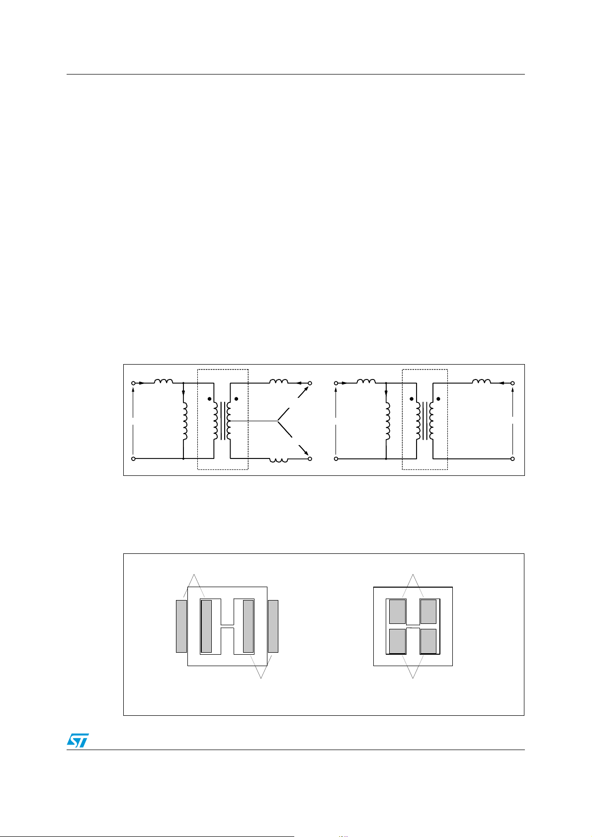
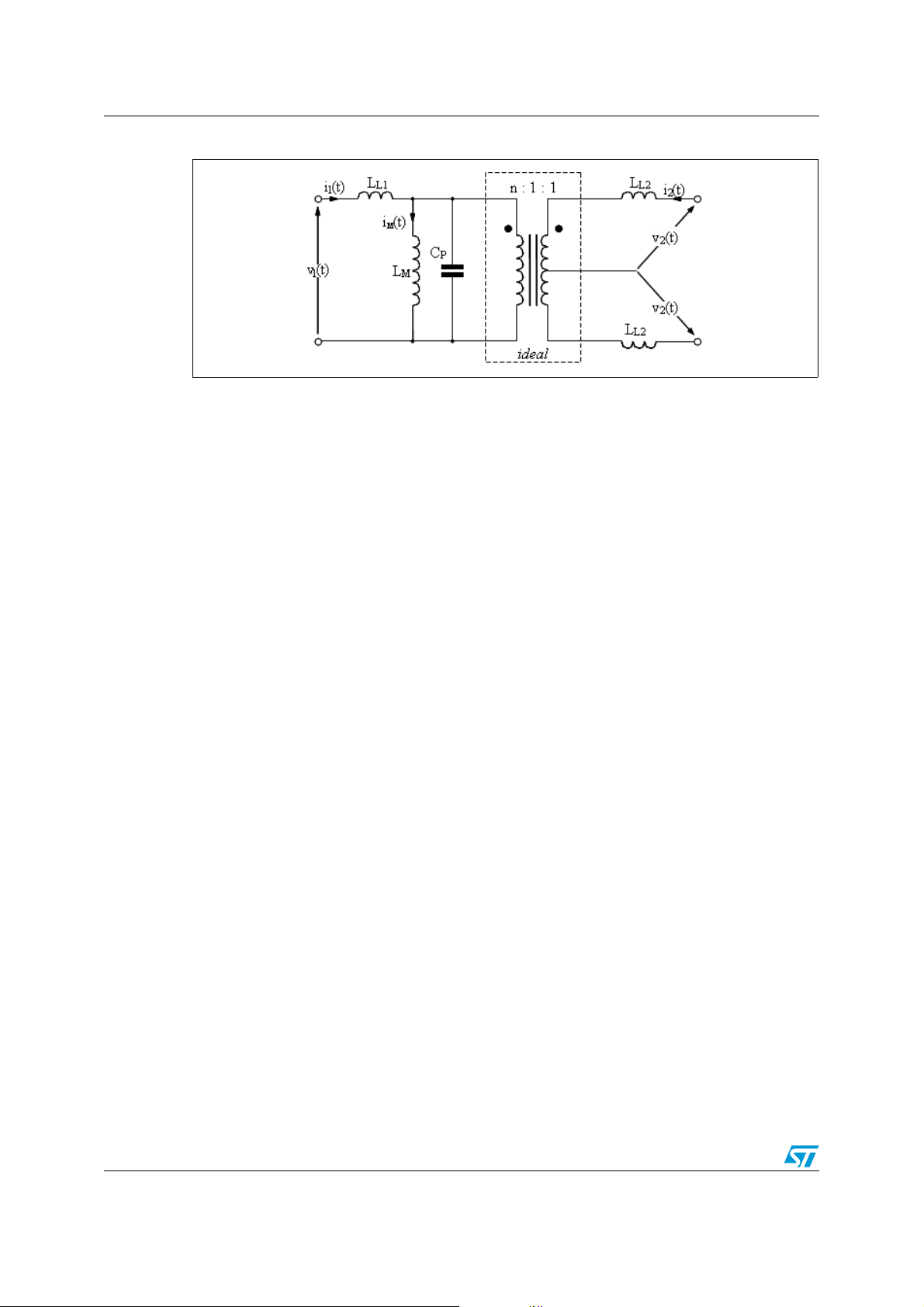
Figure 5. Equivalent schematic of a real transformer (left, tapped secondary; right, single
secondary) . . . . . . . . . . . . . . . . . . . . . . . . . . . . . . . . . . . . . . . . . . . . . . . . . . . . . . . . . . . . . . 9
Figure 6. Example of high-leakage magnetic structures (cross-section) . . . . . . . . . . . . . . . . . . . . . . . 9
Figure 7. Equivalent schematic of a transformer including parasitic capacitance . . . . . . . . . . . . . . . 12
Figure 8. Power MOSFET totem-pole network driving a resonant tank circuit in a half-bridge
converter . . . . . . . . . . . . . . . . . . . . . . . . . . . . . . . . . . . . . . . . . . . . . . . . . . . . . . . . . . . . . . . 13
Figure 9. Detail of Q1 ON-OFF and Q2 OFF-ON transitions with soft-switching for Q2 . . . . . . . . . . 14
Figure 10. Q2 gate voltage at turn-on: with soft-switching . . . . . . . . . . . . . . . . . . . . . . . . . . . . . . . . . . 14
Figure 11. Q2 gate voltage at turn-on: with hard-switching (no ZVS) . . . . . . . . . . . . . . . . . . . . . . . . . 14
Figure 12. Q1 ON-OFF and Q2 OFF-ON transitions with hard switching for Q2 and recovery for
DQ1 . . . . . . . . . . . . . . . . . . . . . . . . . . . . . . . . . . . . . . . . . . . . . . . . . . . . . . . . . . . . . . . . . . 16
Figure 13. Bridge leg transitions in the neighborhood of inductive-capacitive regions boundary . . . . 17
Figure 14. Bridge leg transitions under no-load conditions . . . . . . . . . . . . . . . . . . . . . . . . . . . . . . . . . 19
Figure 15. Reference LLC converter for the analysis of the fundamental operating modes . . . . . . . . 21
Figure 16. Operation at resonance (f = f
Figure 17. Operation above resonance (f > f
Figure 18. Operation above resonance (f > f
load . . . . . . . . . . . . . . . . . . . . . . . . . . . . . . . . . . . . . . . . . . . . . . . . . . . . . . . . . . . . . . . . . . . 27
Figure 19. Operation above resonance (f > f
load . . . . . . . . . . . . . . . . . . . . . . . . . . . . . . . . . . . . . . . . . . . . . . . . . . . . . . . . . . . . . . . . . . . 30
Figure 20. Operation below resonance (f
operation . . . . . . . . . . . . . . . . . . . . . . . . . . . . . . . . . . . . . . . . . . . . . . . . . . . . . . . . . . . . . . . 31
Figure 21. Operation below resonance (f
Figure 22. Capacitive mode operation below resonance (f
Figure 23. No-load operation (cutoff): main waveforms . . . . . . . . . . . . . . . . . . . . . . . . . . . . . . . . . . . . 36
Figure 24. Circuit's equivalent schematic under: no-load conditions . . . . . . . . . . . . . . . . . . . . . . . . . . 38
Figure 25. Circuit's equivalent schematic under: short-circuit conditions. . . . . . . . . . . . . . . . . . . . . . . 38
Figure 26. Converter's startup: main waveforms . . . . . . . . . . . . . . . . . . . . . . . . . . . . . . . . . . . . . . . . . 40
Figure 27. High-side driving with bootstrap approach and bootstrap capacitor charge path. . . . . . . . 41
Figure 28. Frequency compensation with an isolated type 3 amplifier (3 poles + 2 zeros) . . . . . . . . 45
Figure 29. Comparison of gate-charge characteristics with and without ZVS . . . . . . . . . . . . . . . . . . . 48
Figure 30. Equivalent circuit to analyze the transitions of the half-bridge midpoint node when Q2
turns off . . . . . . . . . . . . . . . . . . . . . . . . . . . . . . . . . . . . . . . . . . . . . . . . . . . . . . . . . . . . . . . . 50
Figure 31. Voltage of HB node vs time (see Equation 32). . . . . . . . . . . . . . . . . . . . . . . . . . . . . . . . . . 53
Figure 32. Resonant current vs time (see Equation 34) . . . . . . . . . . . . . . . . . . . . . . . . . . . . . . . . . . . 53
Figure 33. Capacitance associated to the half-bridge midpoint node . . . . . . . . . . . . . . . . . . . . . . . . . 54
Figure 34. C
capacitances vs. half-bridge midpoint's voltage . . . . . . . . . . . . . . . . . . . . . . . . . . . . . 55
oss
Figure 35. Simplified schematic to analyze transition times of the node HB when Q2 turns off . . . . . 56
Figure 36. Schematization of Q2 turn-off transient . . . . . . . . . . . . . . . . . . . . . . . . . . . . . . . . . . . . . . . 57
Figure 37. Input current components in a split-capacitor LLC resonant half-bridge. . . . . . . . . . . . . . . 61
Figure 38. Timing diagram showing currents flow in the converter of Figure 37 . . . . . . . . . . . . . . . . . 61
): main waveforms . . . . . . . . . . . . . . . . . . . . . . . . . . . . . . . 22
R1
): main waveforms in CCMA operation at heavy load 25
R1
): main waveforms in DCMA operation at medium
R1
): main waveforms in DCMAB operation at light
R1
< f < fR1 , R>R
R2
< f < fR1, R>R
R2
): main waveforms in DCMAB
crit
): main waveforms in DCMB2 operation 32
crit
< f < fR1, R<R
R2
): main waveforms . . . 35
crit
4/64
Page 5
AN2644 Classification of resonant converters
1 Classification of resonant converters
Resonant conversion is a topic that is at least thirty years old and where much effort has
been spent in research in universities and industry because of its attractive features: smooth
waveforms, high efficiency and high power density. Yet the use of this technique in off-line
powered equipment has been confined for a long time to niche applications: high-voltage
power supplies or audio systems, to name a few. Quite recently, emerging applications such
as flat panel TVs on one hand, and the introduction of new regulations, both voluntary and
mandatory, concerning an efficient use of energy on the other hand, are pushing power
designers to find more and more efficient AC-DC conversion systems. This has revamped
and broadened the interest in resonant conversion. Generally speaking, resonant
converters are switching converters that include a tank circuit actively participating in
determining input-to-output power flow. The family of resonant converters is extremely vast
and it is not an easy task to provide a comprehensive picture. To help find one's way, it is
possible to refer to a property shared by most, if not all, of the members of the family. They
are based on a "resonant inverter", i.e. a system that converts a DC voltage into a sinusoidal
voltage (more generally, into a low harmonic content ac voltage), and provides ac power to a
load. To do so, a switch network typically produces a square-wave voltage that is applied to
a resonant tank tuned to the fundamental component of the square wave. In this way, the
tank will respond primarily to this component and negligibly to the higher order harmonics,
so that its voltage and/or current, as well as those of the load, will be essentially sinusoidal
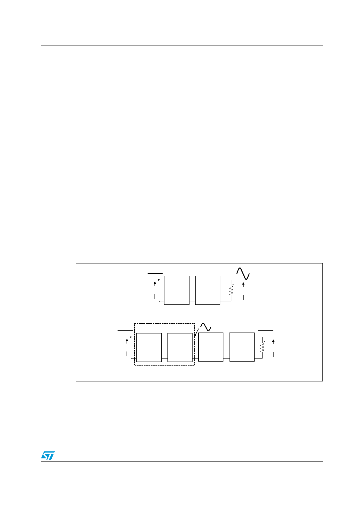
or piecewise sinusoidal. As shown in Figure 2, a resonant DC-DC converter able to provide
DC power to a load can be obtained by rectifying and filtering the ac output of a resonant
inverter.
Figure 2. General block diagram of a resonant inverter, the core of resonant
converters
Resonant
Resonant
Resonant
Resonant
tank circuit
tank circuit
tank circuit
tank circuit
Rectifier
Rectifier
Rectifier
Rectifier
Vout
Vout
Vout
Vout
ac
ac
ac
ac
Low-pass
Low-pass
Low-pass
Low-pass
filter
filter
filter
filter
Vout
Vout
Vout
Vout
dc
dc
dc
dc
Vin
Vin
Vin
Vin
dc
dc
dc
dc
Vin
Vin
Vin
Vin
dc
dc
dc
dc
Resonant Inverter
Resonant Inverter
Resonant Inverter
Switch
Switch
Switch
Switch
network
network
network
network
Switch
Switch
Switch
Switch
network
network
network
network
Resonant Inverter
Resonant Inverter
Resonant Inverter
Resonant
Resonant
Resonant
Resonant
tank circuit
tank circuit
tank circuit
tank circuit
Resonant Converter
Resonant Converter
Resonant Converter
Different types of DC-AC inverters can be built, depending on the type of switch network and
on the characteristics of the resonant tank, i.e. the number of its reactive elements and their
configuration [1].
As to switch networks, we will limit our attention to those that drive the resonant tank
symmetrically in both voltage and time, and act as a voltage source, namely the half-bridge
and the full-bridge switch networks. Borrowing the terminology from power amplifiers,
5/64
Page 6
Classification of resonant converters AN2644
switching inverters driven by this kind of switch network are considered part of the group
called "class D resonant inverters".
As to resonant tanks, with two reactive elements (one L and one C) there are a total of eight
different possible configurations, but only four of them are practically usable with a voltage
source input. Two of them generate the well-known series resonant converter and parallel
resonant converter considered in [2] and thoroughly treated in literature.
With three reactive elements the number of different tank circuit configurations is thirty-six,
but only fifteen can be used in practice with a voltage source input. One of these, commonly
called LCC because it uses one inductor and two capacitors, with the load connected in
parallel to one C, generates the LCC resonant inverter commonly used in electronic lamp
ballast for gas-discharge lamps. Its dual configuration, using two inductors and one
capacitor, with the load connected in parallel to one L, generates the LLC inverter.
As previously stated, for any resonant inverter there is one associated DC-DC resonant
converter, obtained by rectification and filtering of the inverter output. Predictably, the above-
mentioned class of inverters will originate the "class D resonant converters". Considering
off-line applications, in most cases the rectifier block will be coupled to the resonant inverter
through a transformer to guarantee the isolation required by safety regulations. To maximize
the usage of the energy handled by the inverter, the rectifier block can be configured as
either a full-wave rectifier, which needs a center tap arrangement of transformer's secondary
winding, or a bridge rectifier, in which case tapping is not needed. The first option is
preferable with a low voltage / high current output; the second option with a high voltage /
low current output. As to the low-pass filter, depending on the configuration of the tank
circuit, it will be made by capacitors only or by an L-C type smoothing filter. The so-called
"series-parallel" converter described in [2], typically used in high-voltage power supply, is
derived from the previously mentioned LCC resonant inverter. Its dual configuration, the LLC
inverter, generates the homonymous converter, addressed in [3], [4] and [5], that will be the
subject of the following discussion. In particular we will consider the half-bridge
implementation, illustrated in Figure 3, but the extension to the full-bridge version is quite
straightforward.
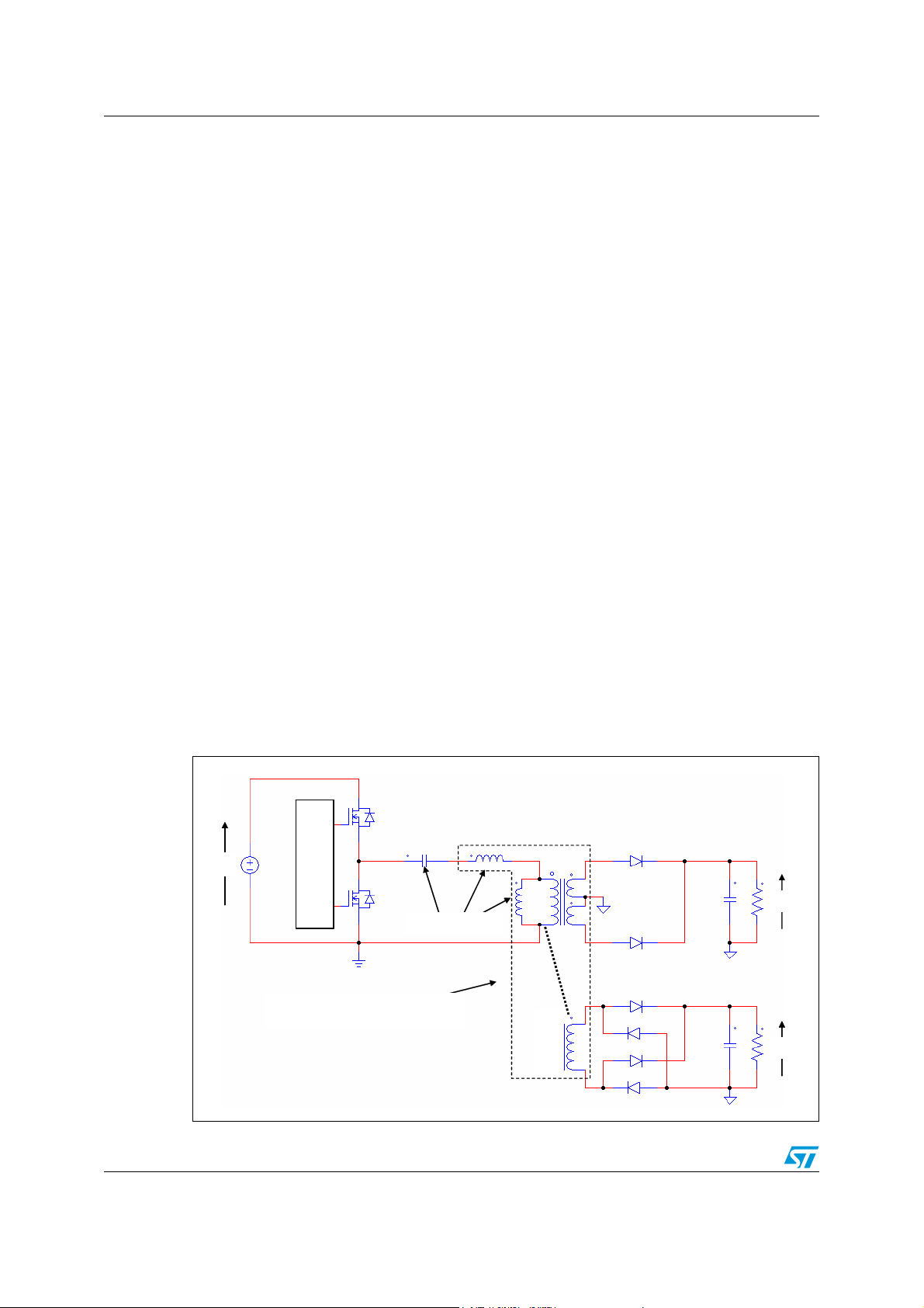
Figure 3. LLC resonant half-bridge schematic
Q1
Cr
VinVin
Preferably integrated into a single
Driver
Driver
Half-bridge
Half-bridge
magnetic structure
Q2
LLC tank circuit
6/64
Ls
Lp
a:1
Center-tapped output with full-wave
(low voltage and high current)
a:1:1
D4
D2
rectification
D1
D2
Single-ended output with bridge
rectification
(high voltage and low current)
D1
D3
R
Vout
R
VoutVout
Page 7

AN2644 The LLC resonant half-bridge converter
In resonant inverters (and converters too) power flow can be controlled by the switch
network either by changing the frequency of the square wave voltage, or its duty cycle, or
both, or by special control schemes such as phase-shift control. In this context we will focus
on power flow control by frequency modulation, that is, by changing the frequency of the
square wave closer to or further from the tank circuit's resonant frequency while keeping its
duty cycle fixed.
2 The LLC resonant half-bridge converter
2.1 General overview
According to another way of designating resonant converters, the LLC resonant half-bridge
belongs to the family of multiresonant converters. Actually, since the resonant tank includes
three reactive elements (Cr, Ls and Lp, shown in Figure 3), there are two resonant
frequencies associated to this circuit. One is related to the condition of the secondary
winding(s) conducting, where the inductance Lp disappears because dynamically shorted
out by the low-pass filter and the load (there is a constant voltage a V
Equation 1
f
R1
1
---------------------------- -=
2π Ls Cr⋅
across it):
out
the other resonant frequency is relevant to the condition of the secondary winding(s) open,
where the tank circuit turns from LLC to LC because Ls and Lp can be unified in a single
inductor:
Equation 2
1
It will be of course f
LLC resonant tank, while f
> fR2. Normally, fR1 is referred to as the resonance frequency of the
R1
is sometimes called the second (or lower) resonance
R2
frequency. The separation between f
f
-------------------------------------------=
R2
2π Ls Lp+()Cr
and fR2 depends on the ratio of Lp to Ls. The larger
R1
this ratio is, the further the two frequencies will be and vice versa. The value of Lp/Ls
(typically > 1) is an important design parameter.
It is possible to show that for frequencies f > f
tank is inductive and that for frequencies f < f
frequency region f
< f < fR1 the impedance can be either inductive or capacitive depending
R2
on the load resistance R. A critical value R
impedance will be capacitive, inductive for R> R
the input impedance of the loaded resonant
R1
the input impedance is capacitive. In the
R2
exists such that if R < R
crit
. For a given tank circuit the value of R
crit
then the
crit
crit
depends on f. More precisely, in [6] it is shown that for any tank circuit configuration (then for
the LLC in particular):
Equation 3
where Zo
R
crit
and Zo∞ are the resonant tank output impedances with the source input short-
0
Zo0Zo∞⋅=
circuited and open-circuited, respectively.
7/64
Page 8
The LLC resonant half-bridge converter AN2644
For certain reasons that will be clarified in the following sections, the LLC resonant
converter is normally operated in the region where the input impedance of the resonant tank
has inductive nature, i.e. it increases with frequency. This implies that power flow can be
controlled by changing the operating frequency of the converter in such a way that a
reduced power demand from the load produces a frequency rise, while an increased power
demand causes a frequency reduction.
The Half-bridge Driver switches the two power MOSFETs Q1 and Q2 on and off in phase
opposition symmetrically, that is, for exactly the same time. This is commonly referred to as
"50% duty cycle" operation even if the conduction time of either power MOSFET is slightly
shorter than 50% of the switching period. In fact, a small deadtime is inserted between the
turn-off of either switch and the turn-on of the complementary one. The role of this deadtime
is essential for the operation of the converter. It goes beyond ensuring that Q1 and Q2 will
never cross-conduct and will be clarified in the next sections as well. For the moment it will
be neglected, and the voltage applied to the resonant tank will be a square-wave with 50%
duty cycle that swings all the way from 0 to V
. Before going any further, however, it is
in
important to make one concept clear.
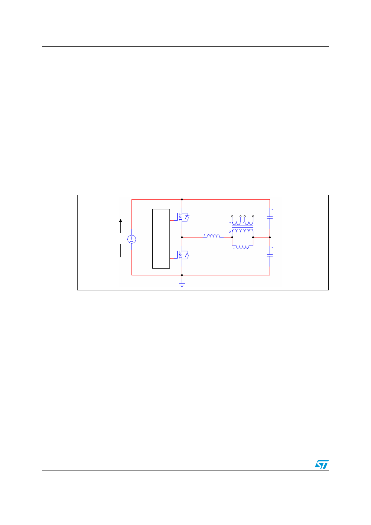
Figure 4. LLC resonant half-bridge with split resonant capacitor
Q1
Q1
Cr / 2
Cr / 2
Ls
Ls
a:1:1
Vin
Vin
Half-bridge
Half-bridge
Half-bridge
Driver
Driver
Driver
Q2
Q2
a:1:1
Lp
Lp
Cr / 2
Cr / 2
A few paragraphs above, the impedance of the tank circuit was mentioned. Impedance is a
concept related to linear circuits under sinusoidal excitation, whereas in this case the
excitation voltage is a square wave.
However, as a consequence of the selective nature of resonant tanks, most power
processing properties of resonant converters are associated with the fundamental
component of the Fourier expansion of voltages and currents in the circuit. This applies in
particular to the input square wave and is the foundation of the First Harmonic
Approximation (FHA) modeling methodology presented in [2] as a general approach and
used in [4] and [5] for the LLC resonant converter specifically. This approach justifies the
usage of the concept of impedance as well as those coming from complex ac circuit
analysis.
Coming back to the input square wave excitation, it has a DC component equal to V
/2. In
in
the LLC resonant tank the resonant capacitor Cr is in series to the voltage source and under
steady state conditions the average voltage across inductors must be zero. As a result, the
DC component V
/2 of the input voltage must be found across Cr which consequently plays
in
the double role of resonant capacitor and DC blocking capacitor.
It is possible to see, especially at higher power levels, a slightly modified version of the LLC
resonant half-bridge converter, where the resonant capacitor is split as illustrated in
Figure 4. This configuration can be useful to reduce the current stress in each capacitor
8/64
Page 9
AN2644 The LLC resonant half-bridge converter
and, in certain conditions, the initial imbalance of the V·s applied to the transformer at start
up (see "Converter's start-up" section). Additionally, it makes the input current to the
converter look like that of a full-bridge converter, as shown in Appendix E, with a resulting
reduction in both the input differential mode noise and the stress of the input capacitor.
Obviously, the currents through Q1 and Q2 will be unchanged. It is easy to recognize that
the two Cr/2 capacitors are dynamically in parallel, so that the total resonant tank's
capacitance is again Cr.
The system appears quite bulky, with its three magnetic components. However, the LLC
resonant topology lends itself well to magnetic integration. With this technique inductors and
transformers are combined into a single physical device to reduce component count, usually
with little or no penalty to the converter's characteristics, sometimes even enhancing its
operation. To understand how magnetic integration can be done, it is worth looking at the
well-known equivalent schematics of a real transformer in Figure 5 and comparing them to
the inductive component set of Figure 3.
Lp occupies the same place as the magnetizing inductance L
primary leakage inductance L
. Then, assuming that we are going to use a ferrite core plus
L1
, Ls the same place as the
M
bobbin assembly, Lp can be used as the magnetizing inductance of the transformer with the
addition of an air gap into the magnetic circuit and leakage inductance can be used to make
Ls.
Figure 5. Equivalent schematic of a real transformer (left, tapped secondary; right,
single secondary)
L
i1(t)
i1(t)
L
L1
L1
iM(t)
iM(t)
L
L
M
M
n : 1
n : 1
ideal
ideal
L
L
L2
L2
i2(t)
i2(t)
v2(t)
v2(t)v2(t)
v1(t)
v1(t)v1(t)
i1(t)
i1(t)
L
L
L1
L1
iM(t)
iM(t)
L
L
M
M
n : 1 : 1
n : 1 : 1
ideal
ideal
L
L
L2
L2
i2(t)
i2(t)
v2(t)
v2(t)v2(t)
v1(t)
v1(t)v1(t)
v2(t)
v2(t)v2(t)
L
L
L2
L2
To do so, however, a leaky magnetic structure is needed, which is contrary to the traditional
transformer design practice that aims at minimizing leakage inductance. The usual
concentric winding arrangement is not recommended here, although higher leakage
inductance values can be achieved by increasing the space between the windings.
Figure 6. Example of high-leakage magnetic structures (cross-section)
Primary
Primary
winding
winding
Primary
Primary
winding
winding
Secondary
Secondary
winding
winding
Windings on separate legs of an EE core
Secondary
Secondary
winding
winding
Side-by-side windings (EE or pot core)Windings on separate legs of an EE core
Side-by-side windings (EE or pot core)
9/64
Page 10

The LLC resonant half-bridge converter AN2644
It is difficult, however to obtain reproducible values, because they depend on parameters
(such as winding surface irregularities or spacer thickness) difficult to control. Other fashions
are recommended, such as placing the windings on separate core legs (using E or U cores)
or side by side on the same leg which is possible with both E and pot cores and shown in
Figure 6. They permit reproducible leakage inductance values, because related to the
geometry and the mechanical tolerances of the bobbin, which are quite well controlled. In
addition, these structures possess geometric symmetry, so they lead to magnetic devices
with an excellent magnetic symmetry.
However, in the real transformer model of Figure 5 there is the secondary leakage
inductance L
that is not considered in the model of Figure 3. The presence of LL2 is not a
L2
problem from the modeling point of view because the transformer's equivalent schematic
can be manipulated so that L
incorporated in L
). This is exactly what has been done in the transformer model shown in
L1
disappears (it is transferred to the primary side and
L2
Figure 3. Then, it is important to underline that Ls and Lp are not real physical inductances
(L
, LM and LL2 are), their numerical values are different (Ls ≠ LL1, Lp ≠ LM), and, finally, the
L1
turn ratio a is not the physical turn ratio n=N
interpretation. L
is the inductance of the primary winding measured with the secondary
s
. Ls and Lp can be given a physical
1/N2
winding(s) shorted, while Lp is the difference between the inductance of the primary winding
measured with the secondary windings open and L
However, L
is not free from side effects. For a given impressed voltage, LL2 decreases the
L2
voltage available on the secondary winding, which carries a current i
.
s
, by the drop LL2·di2/dt.
2
This is an effect that is taken into account by the above mentioned manipulation of the
transformer model. In addition, in multioutput converters, where there is leakage inductance
associated to each output winding, cross-regulation between the various outputs will be
adversely affected because of their decoupling effect.
Finally, there is one more adverse effect to consider in the center-tapped output
configuration. With reference to Figure 3 and 5, when one half-winding is conducting, the
voltage v
(t) externally applied to that half-winding is V
2
(VF is the rectifier forward drop
out+VF
of the conducting diode). With no secondary leakage inductance, this voltage will be found
across the secondary winding of the ideal transformer and then coupled one-to-one to the
nonconducting half-winding. Consequently, the reverse voltage applied to the reverse-
biased rectifier will be 2·V
L
·di2/dt adds up to V
L2
out+VF
the reverse voltage applied to the nonconducting rectifier will be increased by L
. If now we introduce the leakage inductance LL2, the drop
out+VF
. and is reflected to the other half-winding as well. As a result,
·di2/dt.
L2
Note that in case of single-winding secondary with bridge rectification, the voltage applied to
reverse-biased diodes of the bridge is only V
that the negative voltage of the secondary winding is fixed at -V
and is not affected by LL2. The reason is
out+VF
externally and is not
F
determined by internal coupling like in the case of tapped secondary.
It is worth pointing out that the 50% duty cycle operation of the LLC half-bridge equalizes
the stress of secondary rectifiers both in terms of reverse voltage - as just seen - and
forward conduction current. In fact, each rectifier carries half the total output current under
all operating conditions. Then, if compared to similar PWM converters (such as the ZVS
Asymmetrical Half-bridge, or the Forward converter), in the center-tapped output
configuration the equal reverse voltage typically allows the use of lower blocking voltage
rating diodes. This is especially true when using common cathode diodes housed in a single
package. A lower blocking voltage means also a lower forward drop for the same current
rating, and then lower losses.
It must be said, however, that in the LLC resonant converter the output current form factor is
worse, so the output capacitor bank is stressed more. Although the stress level is
10/64
Page 11
AN2644 The LLC resonant half-bridge converter
considerably lower than that in a flyback converter, as shown in Ta bl e 1 , this is one of the
few real drawbacks of the topology.
Table 1. Output stress for LLC resonant half-bridge vs. PWM topologies @ 50% duty cycle
Output current form factors Forward - ZVS AHB LLC resonant HB Flyback (CCM-DCM boundary)
Peak-to-DC ratio ≈1.05÷1.15
Rms-to-DC ratio ≈1
AC-to-DC ratio ≈0.03÷0.09
π
-- -
≈ 1.57=
2
π
---------- -
≈ 1.11=
22
2
π
----- - 1–≈ 0.48=
8
8
-- - 1.63≈
3
8
-- - 1– 1.29≈
3
4
Additional details concerning power losses will be discussed in Analysis of power losses on
page 41.
To complete the general picture on the LLC resonant converter, there is another aspect that
needs to be addressed concerning parasitic components which affect the behavior of the
circuit.
The first parasitic element to consider is the capacitance of the midpoint of the half-bridge
structure, the node common to the source of the high-side power MOSFET and to the drain
of the low-side power MOSFET. Its effect is that the transitions of the half-bridge midpoint
will require some energy and take a finite time to complete. This is linked to the previously
mentioned deadtime inserted between the turn-off of either switch and the turn-on of the
complementary one, and will be discussed in more detail in Section 2.2.
The second parasitic element to consider is the distributed capacitance of transformer's
windings. This capacitance, which exists for both the primary and the secondary windings,
in combination with windings' inductance, originates what is commonly designated as the
transformer "self-resonance". In addition to this capacitance one needs to consider also the
junction capacitance of the secondary rectifiers, which adds up to that of the secondary
windings and lowers the resulting self-resonance frequency (loaded self-resonance).
The effect of all this parasitic capacitance can be modeled with a single capacitor C
connected in parallel to L
turns from LLC to LLCC. This 4
the transformer's loaded self-resonance (f
considerably lower than f
than f
and if the load impedance is high enough, its effect starts making itself felt,
R1
as illustrated in Figure 7. The resonant tank, as a consequence,
M
th
- order tank circuit features a third resonance frequency at
> fR1). When the operating frequency is
the effect of CP is negligible. However, at frequencies greater
LSR
LSR
P
eventually resulting in reversing the transferable power vs. frequency relationship as
frequency approaches f
. Power now increases with the switching frequency, feedback
LSR
becomes positive and the converter loses control of the output voltage. The onset of this
"feedback reversal" in closed-loop operation is revealed by a sudden frequency jump to its
maximum value as the load falls below a critical value (i.e. the frequency exceeds a critical
value) and a simultaneous output voltage rise.
In some way, either appropriately choosing the operating frequency range (<< f
increasing f
, the converter must work away from feedback reversal. This usually sets the
LSR
LSR
) or
practical upper limit to a converter's operating frequency range.
11/64
Page 12
The LLC resonant half-bridge converter AN2644
Figure 7. Equivalent schematic of a transformer including parasitic capacitance
2.2 The switching mechanism
Still another way of classifying resonant converters would include the LLC resonant halfbridge in the family of "resonant-transition" converters. This nomenclature refers to the fact
that in this class of converters power switches are driven in such a way that a resonant tank
circuit is stimulated to create a zero-voltage condition for them to turn-on.
To understand how this can be achieved in the LLC half-bridge, it is instructive to consider
the circuits illustrated in Figure 8 where the switches Q1 and Q2 that generate the square
wave input voltage to the resonant tank are power MOSFETs. Their body diodes DQ1, DQ2
are pointed out because they play an important role. In circuit a), the drain-to-source
parasitic capacitances C
changes of the node HB are concerned, the parasitic capacitances Cgd and Cds are
effectively in parallel, then Cgd+Cds=C
Additionally, other contributors to the parasitic capacitance of the node HB (e.g. that formed
between the case of the power MOSFETs and the heat sink, the intrawinding capacitance of
the resonant inductor, etc.) are lumped together in the capacitor C
C
, is connected between the node HB and a node having a fixed voltage (Vin for C
oss2
ground for C
). Then, as far as voltage changes of the node HB are concerned, C
oss2
effectively connected in parallel to C
together in a single capacitor C
oss1
, C
are pointed out as well. In fact, as far as voltage
oss2
has to be considered.
oss
. Note that C
Stray
and C
oss2
from the node HB to ground, as shown in the circuit b):
HB
. It is convenient to lump all of them
Stray
oss1
oss1
, like
oss1
is
,
Equation 4
C
HB
C
which we will refer to in the following discussion. Note also that C
linear capacitors, i.e. their value is a function of the drain-to-source voltage. It is intended
that their time-related equivalent value will be considered (see Appendix A).
12/64
++=
OSS1COSS2CStray
oss1
and C
oss2
are non-
Page 13
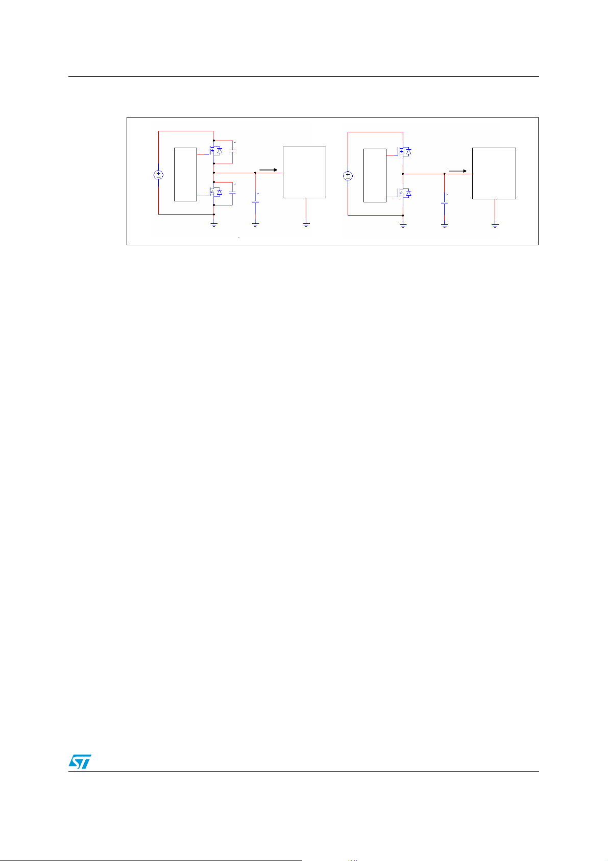
AN2644 The LLC resonant half-bridge converter
Figure 8. Power MOSFET totem-pole network driving a resonant tank circuit in a
half-bridge converter
Q1
Q1
Coss
Coss
1
1
DQ1
Vin
Vin
Node
Node
HB
HB
Q2
Q2
HB Driver
HB Driver
DQ1
DQ2
DQ2
Coss
Coss
2
2
C
C
Stray
Stray
I
IRI
R
R
Resonant
Resonant
Tank &
Tank &
Load
Load
Vin
Vin
Q1
Q1
DQ1
DQ1
Node
Node
HB
HB
Q2
Q2
HB Driver
HB Driver
DQ2
DQ2
C
C
HB
HB
I
IRI
R
R
Resonant
Resonant
Tank &
Tank &
Load
Load
a)
a)
b)
b)
As previously stated, there is no overlap between the conduction of Q1 and Q2.
Additionally, a deadtime T
between the transitions from one state to the other of either
D
switch, where they both are open, is intentionally inserted. It is intended that when Q1 is
closed and Q2 is open, the voltage applied to the resonant tank circuit is positive. Similarly
we will define as negative the voltage applied to the resonant tank circuit when Q1 is open
and Q2 is closed. Consistently with two-port circuits sign convention, the input current to the
resonant tank, I
Let us assume Q1 closed and Q2 open. It is then I
to the circuit is positive (V
reactive elements. Let us suppose that I
instant t
when Q1 opens, and refer to the timing diagram of Figure 9.
0
The current through Q1 falls quickly and becomes zero at t = t
, will be positive if entering the circuit, negative otherwise.
R
= I(Q1). Despite that the voltage applied
= Vin), IR can flow in either direction since we are in presence of
HB
is entering the tank circuit (positive current) in the
R
R
. Q2 is still open and IR must
1
keep on flowing almost unchanged because of the inductance of the resonant tank that acts
as a current flywheel. The electrical charge necessary to sustain I
C
, initially charged at Vin, which will be now discharged. Provided IR(t1) is large enough,
HB
the voltage of the node HB will then fall at a certain rate until t = t
will come initially from
R
, when its voltage
2
becomes negative and the body diode of Q2, DQ2, becomes forward biased, thus clamping
the voltage at a diode forward drop V
the remaining part of the deadtime T
DQ2. When this occurs, the voltage across Q2 is -V
input voltage V
. In the end, this is what is called zero-voltage switching (ZVS): the turn-on
in
below ground. IR will go on flowing through DQ2 for
F
until t = t3, when Q2 turns on and its R
D
, a value negligible as compared to the
F
DS(on)
shunts
transition of Q2 is done with negligible dissipation due to voltage-current overlap and with
C
already discharged, there will be no significant capacitive loss either. Note, however,
HB
that there will be nonnegligible power dissipation associated to Q1's turn-off because there
will be some voltage-current overlap during the time interval t
- t1.
0
13/64
Page 14
The LLC resonant half-bridge converter AN2644
Figure 9. Detail of Q1 ON-OFF and Q2 OFF-ON transitions with soft-switching for
Q2
Dead-time
Dead-timeDead-time
t0–t1Q1 current fall time;
t0–t1Q1 current fall time;
voltage-current overlap for Q1
voltage-current overlap for Q1
Node HB transition time
Node HB transition time
t
t
0–t2
0–t2
t
t
Q2’ body diode conduction time
Q2’ body diode conduction time
2–t3
2–t3
Vc = Resonant capacitor voltage
Vc = Resonant capacitor voltage
VHB= Node HB voltage
VHB= Node HB voltage
IR= Tank circuit’s current
IR= Tank circuit’s current
I(Lp) = Lp (magnetizing) current
I(Lp) = Lp (magnetizing) current
I(Q1) = MOSFET Q1 current
I(Q1) = MOSFET Q1 current
I(CHB) = CHBcurrent
I(CHB) = CHBcurrent
V
V
HB
HB
I
I
R
R
Q2 OFF
Q2 OFF
Q1’s current
Q1’s current
falls to zero
falls to zero
Q1 ON
Q1 ON
Low turn-off losses
Low turn-off losses
I(Q1)
I(CHB)
I(Q1)
I(CHB)
Q1 OFF
Q1 OFF
Q2 OFF
Q2 OFF
Tank circuit’s current
Tank circuit’s current
is positive
is positive
t
t
0 t1t2 t3
0 t1t2 t3
Q1 OFF
Q1 OFF
Q2 ON
Q2 ON
Q2 is switched on with essentially
Q2 is switched on with essentially
zero drain-to-source volt age: ZVS!
zero drain-to-source volt age: ZVS!
Magnetizing current equals
Magnetizing current equals
tank circuit’s current
tank circuit’s current
HB node’s parasitic capa-
HB node’s parasitic capacitance discharge current
citance discharge current
There is an additional positive side effect in turning on Q2 with zero drain-to-source voltage.
It is the absence of the Miller effect, normally present in power MOSFETs at turn-on when
hard-switched. In fact, as the drain-to-source voltage is already zero when the gate is
supplied, the drain-to-gate capacitance Cgd cannot "steal" the charge provided to the gate.
The so-called "Miller plateau", the flat portion in the gate voltage waveform, as well as the
associated gate charge, is missing here and less driving energy is therefore required. Note
that this property provides a method to check if the converter is running with soft-switching
or not by looking at the gate waveform of Q2 (which is more convenient because it is sourcegrounded), as shown in Figure 10 and 11.
Figure 10. Q2 gate voltage at turn-on: with
soft-switching
HB node is falling down
here; current due to Cgd
With similar reasoning it is possible to understand that the same ZVS mechanism occurs to
Q1 when it turns on if I
is flowing out of the resonant tank circuit (negative current).
R
In the end we can conclude that, if the tank current at the instant of half-bridge transitions
has the same sign as the impressed voltage, both switches will be "soft-switched" at turn-on,
i.e. turned on with zero voltage across them (ZVS). It is intuitive that this sign coincidence
Figure 11. Q2 gate voltage at turn-on: with
hard-switching (no ZVS)
Current injection through
Cgd due to hard-switching
Miller effect
14/64
Page 15

AN2644 The LLC resonant half-bridge converter
occurs if the tank current lags the impressed voltage (e.g. it is still positive while voltage has
already gone to zero), which is a condition typical of inductors. In other words, ZVS occurs if
the resonant tank input impedance is inductive. The frequency range where tank current
lags the impressed voltage is therefore called the "inductive region".
It is worth emphasizing the essential role of DQ1 and DQ2 in ensuring continuity to current
flow and clamping the voltage swing of the node HB at V
and -VF respectively (the LLC
in+VF
resonant half-bridge belongs to the family of ZVS clamped-voltage topologies). Power
MOSFETs, with their inherent body diodes are therefore the best suited power switches to
be used in this converter topology. Other types of switches, such as BJT or IGBT, would
need the addition of external diodes.
Going back to the state when Q1 is closed and Q2 open, let us now assume that at the
instant t
when Q1 opens, current is flowing out of the resonant tank towards the input
0
source, i.e. it is negative. This operation is shown in the timing diagrams of Figure 12.
With Q1 now open the current will go on flowing through DQ1 throughout the deadtime, and
will eventually be diverted through Q2 only when Q2 closes at t = t
, the end of the
1
deadtime. As far as Q1 is concerned, then, there will be no loss associated to turn-off
because the voltage across it does not change significantly (it is essentially the same
situation seen at turn-on when the converter works in the inductive region).
Q2, instead, will experience now a totally different situation. As DQ1 is conducting during
the deadtime, the voltage across Q2 at t = t
considerable voltage-current overlap but the energy of C
R
happens in PWM-controlled converters at turn-on. The associated power dissipation
½C
as well. In this respect, it is a "hard-switching" condition identical to what normally
DS(on)
2
f may be considerably higher than that normally dissipated under "soft-switching"
HBVin
equals Vin+VF so that there will be not only a
1
will be dissipated inside its
HB
conditions and this may easily lead to Q1 overheating, since heat sinking is not usually sized
to handle this abnormal condition.
In addition to that, at t = t
the body diode of Q1, DQ1, is conducting current and its voltage
1
is abruptly reversed by the node HB being forced to ground by Q2. Hence, DQ1 will keep its
low impedance and there will be a condition equivalent to a shoot-through between Q1 and
Q2 until it recovers (at t = t
).
2
It is well-known the power MOSFET's body diodes do not have brilliant reverse recovery
characteristics. Hence DQ1 will undergo a reverse current spike large in amplitude (it can
be much larger than the forward current it was carrying at t=t
) and relatively long in duration
1
(in the hundred ns) that will go through Q2 as well. This spike, in fact, cannot flow through
the resonant tank because Ls does not allow for abrupt current changes.
This is a potentially destructive condition not only because of the associated power
dissipation that adds up to the others previously considered, but also due to the current and
voltage of DQ1 which are simultaneously high during part of its recovery. In fact, there will
be an extremely high dv/dt (many tens of V/ns!) experienced by Q1 as DQ1 recovers and
the voltage of the node HB goes to zero. This dv/dt may exceed Q1 rating and lead to an
immediate failure because of the second breakdown of the parasitic bipolar transistor
intrinsic in power MOSFET structure. Finally, it is also possible that Q1 is parasitically turned
on if the current injected through its Cgd and flowing through the gate driver's pull down,
which is holding the gate of Q1 low, is large enough to raise the gate voltage close to the
turn-on threshold (see the spike after turn-off in the graph of Figure 11). This would cause a
lethal shoot-through condition for the half-bridge leg.
An additional drawback of this operation is the large and energetic negative voltage spikes
induced by the recovery of DQ1 because of the unavoidable parasitic inductance of the PCB
15/64
Page 16
The LLC resonant half-bridge converter AN2644
subject to its di/dt, which may damage any control IC coupled to the half-bridge leg, not to
mention the big EMI generation.
Similarly, it is possible to show that the same series of adverse events will happen to Q1 and
Q2, with exchanged roles, when Q2 is turned off if I
is flowing into the resonant tank circuit
R
(positive current).
The obvious conclusion is that, if the tank current and the impressed voltage at the instant of
half-bridge transitions have opposite signs, both switches will be hard-switched and the
reverse recovery of their body diodes will be invoked, with all the resulting negative effects. It
is intuitive that this sign opposition occurs if the tank current leads the impressed voltage,
which is typical of capacitors and then occurs if the resonant tank input impedance is
capacitive. This kind of operation is often termed "capacitive mode" and the frequency range
where tank current leads the impressed voltage is called the "capacitive region".
Figure 12. Q1 ON-OFF and Q2 OFF-ON transitions with hard switching for Q2 and
recovery for DQ1
Dead-time
Dead-time
t0–t1Q2’ body diode conduction time;
t0–t1Q2’ body diode conduction time;
coinciding with dead-time
coinciding with dead-time
Q1’s body diode recovery time
Q1’s body diode recovery time
t
t
1–t2
1–t2
Vc = Resonant capacitor voltag e
Vc = Resonant capacitor voltag e
VHB= Node HB voltage
VHB= Node HB voltage
IR= Tank circuit’s current
IR= Tank circuit’s current
I(Lp) = Lp (magnetizing) c urrent
I(Lp) = Lp (magnetizing) c urrent
I(Q1) = MOSFET Q1 current
I(Q1) = MOSFET Q1 current
V
V
HB
HB
Node HB voltage
Node HB voltage
I
I
R
R
Q1 ON
Q1 ON
Q2 OFF
Q2 OFF
I(Q1)
I(Q2)
I(Q1)
I(Q2)
Tank circuit’s current
Tank circuit’s current
is negative
is negative
Q1 OFF
Q1 OFF
Q2 OFF
Q2 OFF
t
t
0 t1t2
0 t1t2
Q1 OFF
Q1 OFF
Q2 ON
Q2 ON
Q2 is hard-switchedQ1 has soft turn-off
Q2 is hard-switchedQ1 has soft turn-off
Resonant capacitor voltage
Resonant capacitor voltage
High dv/dt
High dv/dt
Q1’s body diode
Q1’s body diode
is recovered
is recovered
Current is circulating
Current is circulating
through Q1’s body diode
through Q1’s body diode
Then, the converter must be operated in the region where the input impedance is inductive
(the inductive region), that is, for frequencies f > f
load resistance R is such that R> R
. This is a necessary condition in order for Q1 and Q2
crit
to achieve ZVS, which is evidently a crucial point for the good operation of the LLC resonant
half-bridge.
To summarize, ZVS brings the following benefits:
1. low switching losses: either high efficiency can be achieved if the half-bridge is
operated at a not too high switching frequency (for example < 100 kHz) or high
switching frequency operation is possible with a still acceptably high efficiency
(definitely out of reach with a hard-switched converter);
2. reduction of the energy needed to drive Q1 and Q2, thanks to the absence of Miller
effect at turn-on. Not only is turn-on speed unimportant because there is no voltagecurrent overlap but also gate charge is reduced, then a small source capability is
required from the gate drivers.
3. low noise and EMI generation, which minimizes filtering requirements and makes this
converter extremely attractive in noise-sensitive applications.
4. all of the above-mentioned adverse effects of capacitive mode, which not only impair
efficiency but also jeopardize the converter, are prevented.
16/64
or in the range fR2 < f < fR1 provided the
R1
Page 17
AN2644 The LLC resonant half-bridge converter
Note, however, that working in the inductive region is not a sufficient condition in order for
ZVS to occur.
In the above discussion, it has been said that the voltage of the node HB could swing from
V
to zero "provided IR is large enough". Of course the same holds if we consider node HB's
in
swing from zero up to V
is that the associated inductive energy level of the resonant tank circuit is maintained at the
expense of the energy contained in the capacitance C
greater than that owned by C
the node HB will be able to reach -V
. What actually happens when Q1 turns off with positive IR current
in
2
) is
R
HB
. If the inductive energy (∝ I
(∝ V
2
) CHB will be completely depleted and the voltage of
in
, injecting DQ2 and allowing Q2 to turn-on with
F
HB
essentially zero drain-to-source voltage. Similarly, when Q2 turns off with negative current,
part or all of the associated inductive energy will be transferred to C
inductive energy is greater than that needed to charge C
up to Vin+VF, the node HB will be
HB
. If the available
HB
allowed to swing all the way up until DQ1 is injected, thus clamping the voltage, and Q1 will
be able to turn-on with essentially zero drain-to-source voltage.
Seen from a different perspective, the inductive part of the tank circuit resonates with C
and this is the origin of the term "resonant transition" used for designating resonant
converters having this property. This "parasitic" tank circuit active during transitions is
formed by C
with the series inductance Ls if during the half-bridge transition there is
HB
current circulating on the secondary side (so that Lp is shorted out) or with the total
inductance Ls + Lp if there is no current conduction on the secondary side.
Figure 13. Bridge leg transitions in the neighborhood of inductive-capacitive
Q1 ON
Q1 ON
Q1 ON
Q2 OFF
Q2 OFF
Q2 OFF
V
V
V
HB
HB
HB
IRI(Lp)
IRI(Lp)
IRI(Lp)
V
V
V
HB
HB
HB
IRI(Lp)
IRI(Lp)
IRI(Lp)
regions boundary
Q1 OFF
Q1 OFF
Q1 OFF
Q1 OFF
Q1 OFF
Q1 OFF
Q2 OFF
Q2 OFF
Q2 OFF
Q2 ON
Q2 ON
Q2 ON
Q1’s body diode conduction
Q1’s body diode conduction
Q1’s body diode conduction
Q2 is hard switched
Q2 is hard switched
Q2 is hard switched
Q1’s body diode is recovered
Q1’s body diode is recovered
Q1’s body diode is recovered
IR = 0
IR = 0
IR = 0
a)
a)
a)
Q1 ON
Q1 ON
Q1 ON
Q1 OFF
Q1 OFF
Q2 OFF
Q2 OFF
Q2 OFF
Q1 OFF
Q2 OFF
Q2 OFF
Q2 OFF
Q2 is hard switched
Q2 is hard switched
Q2 is hard switched
c)
c)
c)
Q1 OFF
Q1 OFF
Q1 OFF
Q2 ON
Q2 ON
Q2 ON
IR = 0
IR = 0
IR = 0
VHB= Node HB
VHB= Node HB
VHB= Node HB
voltage
voltage
voltage
IR= Tank circuit’s
IR= Tank circuit’s
IR= Tank circuit’s
current
current
current
I(Lp) = Lp (magnetizing)
I(Lp) = Lp (magnetizing)
I(Lp) = Lp (magnetizing)
current
current
current
VHB= Node HB
VHB= Node HB
VHB= Node HB
voltage
voltage
voltage
IR= Tank circuit’s
IR= Tank circuit’s
IR= Tank circuit’s
current
current
current
I(Lp) = Lp (magnetizing)
I(Lp) = Lp (magnetizing)
I(Lp) = Lp (magnetizing)
current
current
current
V
V
V
HB
HB
HB
IRI(Lp)
IRI(Lp)
IRI(Lp)
V
V
V
HB
HB
HB
IRI(Lp)
IRI(Lp)
IRI(Lp)
Q1 ON
Q1 ON
Q1 ON
Q2 OFF
Q2 OFF
Q2 OFF
Q1 ON
Q1 ON
Q1 ON
Q2 OFF
Q2 OFF
Q2 OFF
Q1 OFF
Q1 OFF
Q1 OFF
Q1 OFF
Q1 OFF
Q1 OFF
Q2 ON
Q2 ON
Q2 ON
Q2 OFF
Q2 OFF
Q2 OFF
Q1’s body diode conduction
Q1’s body diode conduction
Q1’s body diode conduction
Q2 is hard switched
Q2 is hard switched
Q2 is hard switched
Q1’s body diode is recovered
Q1’s body diode is recovered
Q1’s body diode is recovered
b)
b)
b)
Q1 OFF
Q1 OFF
Q1 OFF
Q1 OFF
Q1 OFF
Q1 OFF
Q2 ON
Q2 ON
Q2 ON
Q2 OFF
Q2 OFF
Q2 OFF
Q2 is soft switched
Q2 is soft switched
Q2 is soft switched
d)
d)
d)
IR = 0
IR = 0
IR = 0
IR = 0
IR = 0
IR = 0
HB
,
The above mentioned energy balance considerations, however, are not still sufficient to
guarantee ZVS under all operating conditions. There is an additional element that needs to
be considered, the duration of the deadtime T
.
D
The first obvious consideration is that the duration of the deadtime represents an upper limit
to the time the node HB takes to swing from one rail to the other: in order for the mosfet that
is about to turn on to achieve ZVS (i.e. to be turned on with zero drain-to-source voltage),
the transition has to be completed within T
as depicted in Figure 9. However, the way the
D
17/64
Page 18

The LLC resonant half-bridge converter AN2644
deadtime and ZVS are related is actually more complex and depends on converter's
operating conditions.
It is instructive to see this in Figure 13, which shows typical node HB waveforms occurring
when working in the inductive region but too close to the capacitive region, so that ZVS is
not achieved. They refer to the Q1 →OFF, Q2 → ON transition; those related to the opposite
transition are obviously turned upside down.
● Case a) is very close to the boundary between inductive and capacitive regions. Tank
current reverses just after Q1 is switched off, a portion of node HB ringing appears as a
small "dip", then the tank current becomes negative enough to let the body diode of Q1
start conducting. When Q2 turns on there are capacitive losses and the recovery of the
Q1's body diode with all the related issues.
● Case b) is slightly more in the inductive region but still I
crosses zero within the
R
deadtime. The node HB ringing becomes larger and the body diode of Q1 still conducts
for a short time and its recovery is invoked as Q2 turns on.
● Case c) Is even more in the inductive region but still not sufficiently away from the
capacitive-inductive boundary. The ringing of the node HB is large enough to reach
zero but I
reverses within the deadtime and the voltage goes up again. At the end of
R
the deadtime the voltage does not reach Vin, hence the body diode of Q1 does not
conduct and Q2, when turned on, will experience only capacitive losses.
● Case d) Is further in the inductive region and I
crosses zero nearly at the end of the
R
deadtime. Q2 is now almost soft-switched with no losses. This can be considered as
the boundary of the operating region where ZVS can be achieved with the given
duration of T
.
D
Note that the resonant tank's current during node HB ringing is lower than the one flowing
through Lp. This means that their difference is flowing into the transformer and,
consequently, that one of the secondary half-windings is conducting. Therefore, C
HB
is
resonating with Ls only.
This analysis shows that there is a "border belt" in the inductive region, close to the
boundary with the capacitive region (f
< f < fR1, R = R
R2
) and that as converter's operation
crit
is moved away from the capacitive-inductive boundary and pushed more deeply in the
inductive region there is a progressive behavior change from hard-switching to softswitching. In the cases a and b the inductive energy in the resonant tank is too small to let
the node HB even swing "rail-to-rail"; moving away from the boundary, as shown in case c,
the energy is higher and allows a rail-to-rail swing, but it is not large enough to keep the
node HB "hooked" to the rail throughout the deadtime T
. If the converter is operated in this
D
border belt, Q1 and Q2 will be hard-switched at turn-on and, in cases such as case a and
case b, the body diode of the just turned off power MOSFET is injected and then recovered
as the other power MOSFET turns on.
Case b and, especially, case c highlight that it is possible to look at the deadtime T
from another standpoint: looking at those waveforms, one might conclude that the current I
also
D
R
at the beginning of the deadtime is too low or, conversely, that the deadtime is too long. In
case c, for example, if the dead-time had been approximately half the value actually shown,
Q2 would have been soft-switched at turn-on. Of course, the more appropriate interpretation
depends on whether T
is fixed or not.
D
These cases are related to heavy load conditions.
Figure 14 shows a case typical of no-load conditions, where ZVS is not achieved because of
a too slow transition of the node HB so that it does not swing completely within the deadtime
T
. In this case the situation seems less stressful than operating in the capacitive region.
D
18/64
Page 19
AN2644 The LLC resonant half-bridge converter
There is no body diode conduction and, consequently, no recovery. Q1 will be almost softswitched at turn-off, while Q2 will have capacitive losses at turn-on. It is true that the turn-on
voltage is lower than V
, thus the associated energy of CHB is lower, but at no-load the
in
operating frequency is usually considerably higher than in the capacitive region, then these
power losses may easily overheat Q1 and Q2. Finally, note in Figure 14 that I(Lp) is exactly
superimposed on I
, then the secondary side of the transformer is open and CHB is
R
resonating with the total inductance Ls+Lp.
Figure 14. Bridge leg transitions under no-load conditions
V
V
V
HB
HB
HB
IRI(Lp)
IRI(Lp)
IRI(Lp)
Q1 ON
Q1 ON
Q2 OFF
Q2 OFF
Q1 OFF
Q1 OFF
Q2 OFF
Q2 OFF
Q1 OFF
Q1 OFF
Q2 ON
Q2 ON
Q2 is hard switched
Q2 is hard switched
Q2 is hard switched
VHB= Node HB voltage
VHB= Node HB voltage
IR= Tank circuit’s current
IR= Tank circuit’s current
I(Lp) = Lp (magnetizing) current
I(Lp) = Lp (magnetizing) current
From what we have seen we can conclude that the conditions in order for the half-bridge
switches to achieve ZVS are:
1. Under heavy load conditions, as one switch turns off, the tank current must have the
same sign as the impressed voltage and be large enough so that both the rail-to-rail
transition of the node HB is completed and the current itself does not reverse before the
end of the deadtime, when the other switch turns on.
2. With no-load, the tank current at the moment one switch turns off (which has definitely
the same sign as the impressed voltage) must be large enough to complete the node
HB transition within the deadtime, before the other switch turns on.
Both conditions can be translated into specifying a minimum current value I
to be switched when either power MOSFET turns off. In general, different I
that needs
Rmin
values are
Rmin
needed to ensure ZVS at heavy load and at no-load. One can simply pick the greater one to
ensure ZVS under any operating condition by design. On the other hand, this minimum
required amount of current is to the detriment of efficiency.
At light or no-load a significant current must be kept circulating in the tank circuit, just to
maintain ZVS, in spite of the current delivered to the load that is close to zero or zero. Using
ac-analysis terminology, a certain amount of reactive energy is required even with no active
energy.
Finally, also at heavy load the value of I
to be specified is the result of a trade-off. In fact,
Rmin
its value is directly related to the turn-off losses of both Q1 and Q2. The higher the switched
current is, the larger the switching loss due to voltage-current overlap will be.
The discussion on the switching mechanism has been focused on the primary-side
switches, and the conditions in order for them to achieve soft-switching (ZVS at turn-on,
precisely) have been found. One important merit of the LLC resonant converter is that also
the rectifiers on the secondary side are soft-switched. They feature zero-current switching
(ZCS) at both turn-on and turn-off. In fact, at turn-on the initial current is always zero and
ramps up with a relatively low di/dt, so that forward recovery does not come into play. At
turn-off they become reverse biased when their forward current is already zero, so that their
19/64
Page 20

The LLC resonant half-bridge converter AN2644
reverse recovery is not invoked. This topic will be addressed in Section 2.3, where it will be
shown that this property is inherent in the topology, hence it occurs regardless of converter's
design or operating conditions.
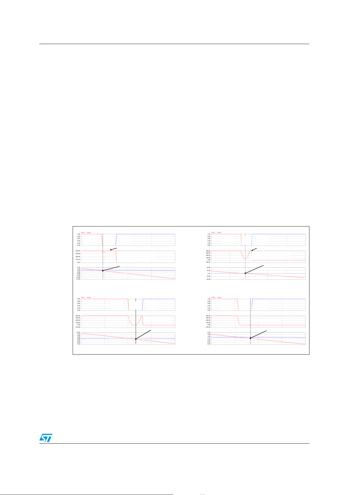
2.3 Fundamental operating modes
The LLC resonant half-bridge converter features a considerable number of different
operating modes, which stem from its multiresonant nature. Essentially, the term
"multiresonant" means that the configuration of the resonant tank may change within a
single switching cycle. We have seen that there are two resonant frequencies, one (the
higher) associated to either of the secondary rectifiers conducting, the lower one associated
to both rectifiers non-conducting. Then, depending on the input-to-output voltage ratio, the
output load and the characteristics of the resonant tank circuit, the secondary rectifiers can
be always conducting (with the exception of a single point in time), which is referred to as
CCM (Continuous Conduction Mode) like in PWM converters, or there can be finite time
intervals during which neither of the secondary rectifiers is conducting. This will obviously be
called a DCM (Discontinuous Conduction Mode) operating mode.
Different kinds of CCM and DCM operating modes exist, although not all of them can be
seen in a given converter, some are not even recommended, like those associated with
capacitive mode operation. However, in all CCM modes the parallel inductance Lp is always
shunted by the load resistance reflected back to the primary side, so that it never
participates in resonance, rather it acts as an additional load to the remaining LC resonant
circuit. Similarly, in all DCM modes, there will be some finite time intervals where Lp, being
no longer shunted from the secondary side, becomes part of resonance.
In the following we will consider four fundamental operating modes and use the
nomenclature defined in [3]:
1. Operation at resonance, when the converter works exactly at f = f
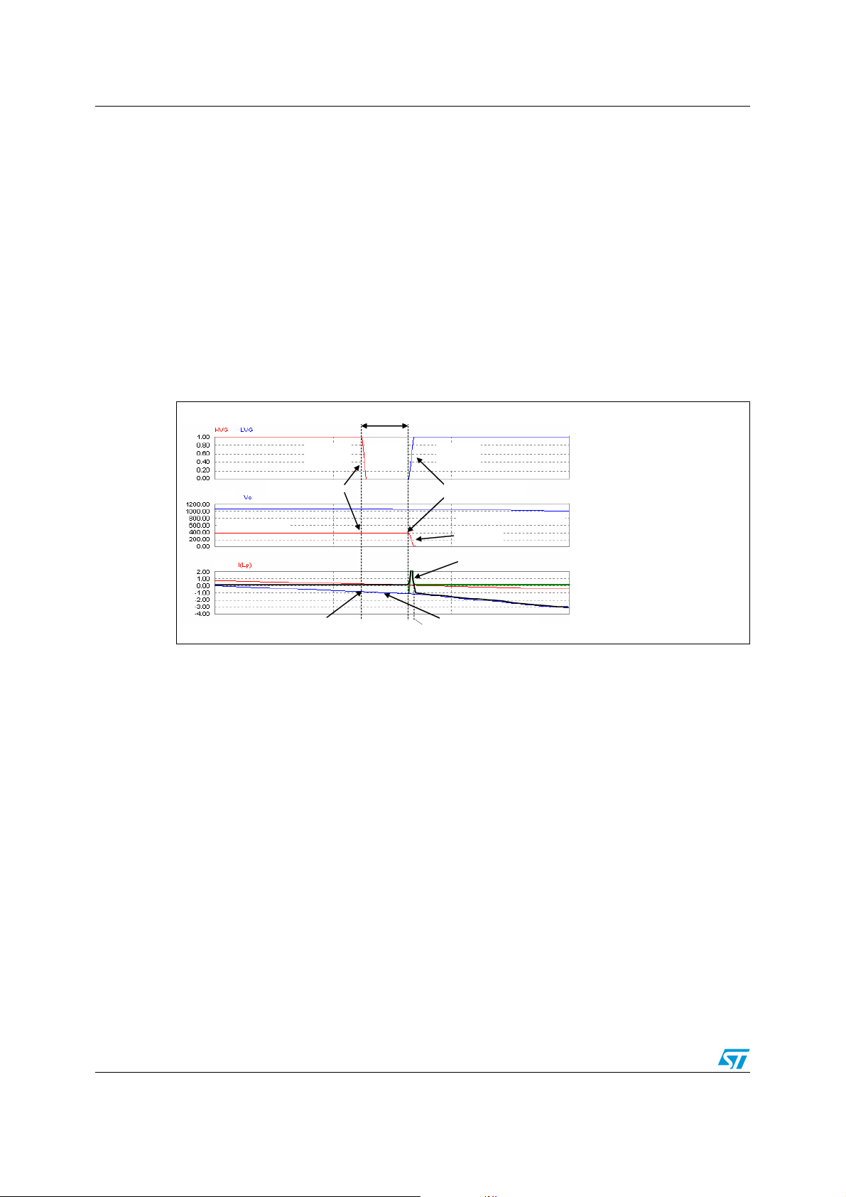
2. Above-resonance operation, when the converter works at a frequency f > f
R1
;
. Moving
R1
away from resonance, we will consider three sub-modes:
a) CCMA operation at heavy load;
b) DCMA operation at medium load;
c) DCMAB operation at light load;
3. Below-resonance operation, when the converter works at a frequency f
a load resistor R > R
. Moving away from resonance, we will consider two sub-modes:
crit
< f < fR1 with
R2
a) DCMAB operation at medium-light load;
b) DCMB operation at heavy load;
4. Below-resonance operation, when the converter works at a frequency f
a load resistor R < R
(capacitive mode), corresponding to the CCMB operating mode
crit
< f < fR1 with
R2
defined in [3];
In addition, two extreme operating conditions will be considered:
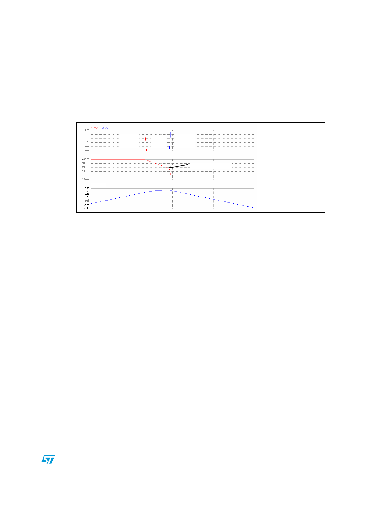
1. No-load operation (cutoff)
2. Output short-circuit operation
It is interesting to point out that, unlike PWM converters where DCM operation is invariably
associated to light load operation and CCM to heavy load operation, in the LLC resonant
converter this combination does not hold.
20/64
Page 21

AN2644 The LLC resonant half-bridge converter
To illustrate the above-mentioned operating modes we will refer to the reference converter
shown in Figure 15. The discussion will start from the inspection of the main waveforms in a
switching cycle, highlighting each subinterval where the circuit assumes a topological state
and deducing the properties of the converter when operated in that mode from those
waveforms. Half-bridge leg transitions are considered instantaneous. Their features have
been already discussed.
Figure 15. Reference LLC converter for the analysis of the fundamental operating
modes
Q1
Driver
+
CTRL
I(Q1)I(Q1)
I(Q2)
Coss1
100 pF
IRI
Q2
R
Coss2
100 pF
22 nF
HB
Ls
200 uH
VcVc
Cr
I(Lp)
Lp
500 uH
8.33:1:1
D1
I(D1)
I(D2)
D2
Cout
24 Vdc
300W
VoutVout
Isolated
feedback
360 to 420
Vdc
VinVin
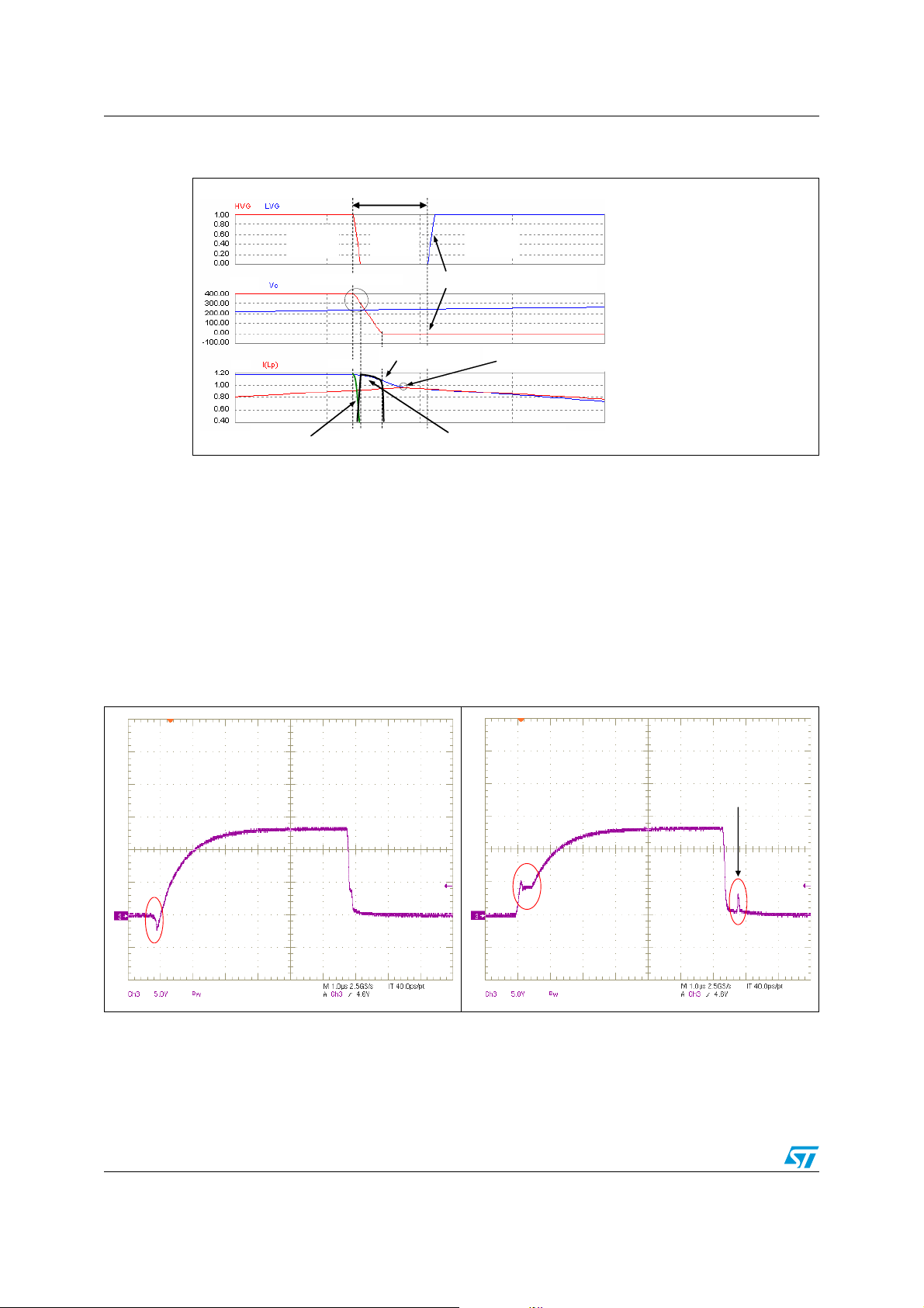
2.3.1 Operation at resonance (f = fR1)
In this operating mode it is possible to distinguish six fundamental time subintervals within a
switching cycle, which are illustrated in Figure 16.
The first subinterval and, then, the instant t
instant when, with Q1 conducting and Q2 open, the tank current I
zero-crossing.
a) t
→ t1. Q1 is ON and Q2 is OFF. This is the "energy taking" phase, when current
0
flows from the input source to the tank circuit, so that energy is positive and both
refills the resonant tank and supplies the load. The operating point of Q1 is in the
first quadrant (current is flowing from drain to source). D2 is reverse-biased with a
voltage -2·V
leakage inductance L
reflected back to the primary side and the voltage across it is fixed at a·V
then, is not participating in resonance and Cr is resonating with Ls only. I
portion of a sinusoid having a frequency f = f
when Q1 is switched off at t=t
decaying. Note that at t=t
b) t
→ t2. This is the deadtime during which both Q1 and Q2 are OFF. At t=t1
1
I(Q1)=I(Lp)=I
swing from V
to flow. The voltage across Lp reverses to -a·V
changes sign. D2 starts conducting while D1 is reverse biased with a negative
voltage approximately equal to 2·V
shown). This phase ends when Q2 is switched on at t=t
c) t
→ t3. Q1 is OFF and Q2 is ON. At t=t2 IR is diverted from DQ2 to the R
2
Q2, so that no significant energy is lost during the turn-on transient. Note that now
(it is actually larger because of the contribution from the secondary
out
is greater than zero and provides the energy to let the node HB
R
to 0, so that the body diode of Q2, DQ2, is injected. This allows IR
in
). D1 is conducting, so Lp is shorted by the output load
L2
1
=I(Lp) and then I(D1)=0.
1 IR
can be chosen quite arbitrarily. We fix t0 as the
0
. During this phase, which ends
R1
has a positive-going
R
out
. Lp,
is a
R
, IR reaches its maximum value, after that it starts
and the slope of its current
out
(plus the contribution from LL2, here not
out
.
2
DS(on)
of
21/64
Page 22

The LLC resonant half-bridge converter AN2644
the operating point of Q2 is in the third quadrant, current is flowing from the source
to drain. D2 keeps on conducting and the voltage across Lp is -a·V
is not participating in resonance and Cr is resonating with Ls only. I
of a sinusoid having a frequency f = f
d) t
→ t4. Q1 is OFF and Q2 is ON. Tank circuit current, which is zero at t=t3
3
. This phase ends when IR=0 at t=t3.
R1
, so that Lp
out
is a portion
R
becomes negative. D1 is non-conducting and its reverse voltage is approximately
2·V
(plus the contribution from LL2, here not shown). Lp's current has a
out
negative slope, so the voltage across Lp must be negative. Since the diode D2 is
conducting, this voltage will be equal to -a·V
resonance, Cr is resonating with Ls only and I
frequency f = f
I
reaches its minimum value, after that it starts increasing. Note that at t=t4
R
I
=I(Lp) and then I(D2)=0.
R
e) t
→ t5. This is the deadtime during which both Q1 and Q2 are OFF. At t=t4
4
I(Q2)=-I(Lp)=-I
swing from 0 to V
. During this phase, which ends when Q2 is switched off at t=t4,
R1
is greater than zero and provides the energy to let the node HB
R
, so that the body diode of Q1, DQ1, is injected. This allows IR
in
to flow back to the input source. The voltage across Lp reverses to a V
. Lp, then, is not participating in
out
is a portion of a sinusoid having a
R
and its
out
current slope changes sign. D1 starts conducting while D2 is reverse biased with
a negative voltage approximately equal to 2·V
here not shown). This phase ends when Q1 is switched on at t=t
(plus the contribution from LL2,
out
.
5
Figure 16. Operation at resonance (f = f
t0t
0
Q1 ON
Q2 OFF
): main waveforms
R1
t1t1t2t
t3t
2
3
Q1 OFF
Q2 ON
t5t
t6t
t4t
5
6
4
Q1 ON
Q2 OFF
I(D1) = D1 currentV(D1) = D1 anode voltageI(Q1) = Q1 currentIR = Tank circuit’s currentVHB = Node HB voltageHVG= Q1 gate
I(D1) = D1 currentV(D1) = D1 anode voltageI(Q1) = Q1 currentIR = Tank circuit’s currentVHB = Node HB voltageHVG= Q1 gate
I(D2) = D2 currentV(D2) = D2 anode voltageI(Q2) = Q2 currentI(Lp) = Lp (magnetizing) currentVc = Resonant capacitor voltageLVG = Q2 gate
I(D2) = D2 currentV(D2) = D2 anode voltageI(Q2) = Q2 currentI(Lp) = Lp (magnetizing) currentVc = Resonant capacitor voltageLVG = Q2 gate
→ t6. Q1 is ON and Q2 is OFF. At t=t5 IR is diverted from DQ1 to the R
f) t
5
Q1, so that no significant energy is lost during the turn-on transient. Note that now
the operating point of Q1 is in the third quadrant, current is flowing from the source
to drain. This phase, along with the preceding one can be referred to as the
"external energy recirculation phase": current is negative (coming out of the input
terminal) despite that the impressed voltage is positive so that the input energy is
22/64
DS(on)
of
Page 23

AN2644 The LLC resonant half-bridge converter
negative, i.e. it is returned to the input source. D1 keeps on conducting and the
voltage across Lp is a·V
resonating with Ls only. I
This phase ends when I
, so that Lp is not participating in resonance and Cr is
out
is a portion of a sinusoid having a frequency f = fR1.
R
=0 at t=t6 and another switching cycle starts.
R
Remarks
1. Parallel inductor Lp never resonates and its current is essentially triangular (note: the
real magnetizing current is sinusoidal and cannot be seen on the oscilloscope). The
LLC converter, then, can be regarded as a series LC resonant half-bridge (composed
by Ls and Cr) that supplies a reactive RL load (composed by Lp and R
ac resistor loading the converter, as defined in [2] and reflected back to the primary
side). This standpoint provides considerable insight into the operation of the converter,
as shown in some of the following remarks.
2. In a resistively loaded series LC tank operating at resonance, the impressed voltage
and the tank current are exactly in-phase, hence the switched current is zero and,
thereby, ZVS cannot be achieved. The effect of adding an inductor (Lp) in parallel to
the resistive load is to provide tank current with the phase shift (lagging) necessary to
switch a current greater than zero, so that ZVS becomes now possible at resonance.
As shown in the diagrams of Figure 16, the tank circuit current lags the impressed
voltage by an angle ϕ equal to:
, the equivalent
ac
Equation 5
–
t
6t4
--------------
ϕ 2π
=
t
–
6t0
so that they have the same sign at half-bridge leg transitions. Furthermore, the
switched currents I
within the deadtimes (t
) and IR(t4) are large enough to complete the HB node swing well
R(t1
, t2) and (t4, t5) respectively. It is not difficult to recognize that
1
the angle ϕ is the phase of the input impedance of the loaded resonant tank evaluated
at f=f
. Additionally, since the impedance of a series LC tank operating at resonance
R1
is zero, it is possible to state that the input impedance of the LLC resonant tank at
resonance equals the impedance of the RL load.
3. Generally speaking, in a series LC tank operating at resonance, the voltage drop
across L is equal in module and opposite in sign to the drop across C at all times (this
is why its impedance is zero). In our specific case the drop across the series Cr-Ls will
be zero, so that it is possible to write the following voltage balance equations:
Equation 6
V
in
------- -
V
=–
in
2
V
in
------- -– aV⋅
–=
2
aV⋅
out
out
Q1 ON, Q2 OFF
Q1 OFF, Q2 ON
both of them resulting in the following relationship:
Equation 7
V
in
------- - aV
2
This is a fundamental property of the LLC resonant half-bridge: operating at f=f
⋅=
out
R1
implies that input and output voltages fulfill (1) and, vice versa, if input and output
voltages meet Equation 7 the converter is operating at f=f
converter operates at resonance or not, for a given output voltage V
. Then, the fact that the
R1
and a given turn
out
23/64
Page 24

The LLC resonant half-bridge converter AN2644
ratio a (n), depends only on the input voltage, not on the load and on the parameters of
the resonant tank. From the design point of view, since V
and V
in
are specified, one
out
can decide the input voltage where to operate at resonance by choosing the turns ratio
a. V
/2=a·V
in
considered as the 1:1 conversion ratio for the LLC resonant half-bridge.
out
4. The logical consequence of LLC converter's ability to operate at resonance
independently of the output load is that the LLC resonant half-bridge can deliver any
power if operated at resonance. This can be seen also in another way. As the
impedance of the series Cr-Ls is zero, the RL load R
//Lp "sees" the impressed
ac
voltage directly or, in other words, it is supplied by an ideal voltage source. This is a
"singularity" in LLC converter's operation, sometimes referred to as the "loadindependent" point, where the usual energy vs. frequency relationship does not hold.
Actually, the inevitable voltage drops across the resistive elements of the real-world
circuit (such as power MOSFETs' R
, winding resistance, secondary rectifier's
DS(on)
drop, etc.) cause a slight dependence of the frequency on the load. Note that this is a
situation analog to that of CCM-operated PWM converters, where duty cycle is ideally
independent of the load, in reality slightly dependent because of losses.
5. Energy is taken from the input source only from t
for less than half the switching period, while from t
to t1, the "energy taking" phase, then
0
to t4 energy recirculates internally
1
to allow energy flow to the load while Q1 is not conducting. This low "duty cycle" of the
input current can be a limiting factor in terms of power handling capability, especially if
the input voltage is low. This consideration suggests the use of the half-bridge topology
in high input voltage applications (e.g. with a PFC front-end, which provides a
400 V input rail). The natural improvement to this limitation is the full-bridge topology,
where phase d) becomes active as well.
6. Tank circuit current lag ϕ originates the external energy recirculation phase from t
to t6
4
during which energy flow is negative (impressed voltage and input current have
opposite signs). This energy subtracts to that drawn from the input during the energy
taking phase a), hence reducing the net energy flow from the input source to the load
each cycle. This energy can be regarded as reactive energy and cos ϕ as the input
power factor. Making ϕ as small as possible (i.e. increasing Lp) would shorten the
duration of the external energy recirculation phase and reduce the amount of reactive
energy, thus improving the energy transfer process. This, however, would also reduce
I
) and IR(t4), hence ϕ can be reduced as long as ZVS is maintained.
R(t1
7. Recalling that the current switched at turn-off by Q1, I
) and by Q2, IR(t4) determine
R(t1
their switching losses, it is straightforward that keeping ϕ to the minimum value that
ensures ZVS of Q1 and Q2 provides an optimum design. Of course, component
tolerance must be adequately accounted for, thus ϕ must be larger than the minimum
required and the typical operation will be suboptimal.
8. The secondary rectifiers D1 and D2 start conducting as Q2 and Q1 turn-off
respectively. The initial current is zero and also its di/dt is low, thus they have a soft
turn-on. D1 and D2 cease to conduct exactly when Q1 and Q2 turn-off, respectively.
These are also the moments when the voltages across D1 and D2 reverse. As a result,
neither D1 nor D2 experience a voltage reversal while conducting a forward current.
Reverse recovery, with all its adverse effects, does not occur. Note that, in this respect,
this is a situation identical to that of a PWM converter operating on the boundary
between CCM and DCM.
2.3.2 Operation above resonance (f > fR1)
In this operating mode the converter exhibits its usual frequency vs. load characteristic. We
will consider three submodes where, in a closed-loop regulated system, CCM operation
24/64
Page 25

AN2644 The LLC resonant half-bridge converter
progressively turns into DCM operation as the output load is reduced and frequency is
moved away from resonance.
CCMA operation at heavy load
Also in this case it is possible to identify six fundamentals subintervals. The relevant
waveforms are illustrated in the timing diagram of Figure 17. Again, t
with Q1 conducting and Q2 open, the tank current I
a) t
→ t1. Q1 is ON and Q2 is OFF. This is the "energy taking" phase. It is identical
0
has a positive-going zero-crossing.
R
to the corresponding phase seen in the operation at resonance with the only
difference that at the end of this phase, at t=t
b) t
→ t2. This is the deadtime during which both Q1 and Q2 are OFF. At t=t1 IR is
1
, it is still IR > I(Lp) and then I(D1)>0.
1
greater than zero and provides the energy to let the node HB swing from V
so that the body diode of Q2, DQ2, is injected. This allows I
changes to a higher negative value, so that it quickly approaches I(Lp), which is
still increasing with the same slope. D1 conducts until I
becomes reverse biased, with a negative voltage equal to 2·V
contribution from L
, here not shown), I(Lp) slope changes sign and D2 starts
L2
conducting. This phase ends when Q2 is switched on at t=t
Tz needed for I
t=t
and not to the duration of the deadtime TD. Here it is Tz = TD just by chance.
1
to hit I(Lp) is related to their values at t=t1 and their slopes after
R
is the instant when,
0
to flow; IR slope
R
equals I(Lp), and then
R
(plus the
out
. Note that the time
2
in
to 0,
Figure 17. Operation above resonance (f > f
at heavy load
t0t
0
Q1 ON
Q2 OFF
): main waveforms in CCMA operation
R1
t1t1t2t
t3t
2
3
Q1 OFF
Q2 ON
t5t
t4t
t6t
5
6
4
Q1 ON
Q2 OFF
I(D1) = D1 currentV(D1) = D1 anode voltageI(Q1) = Q1 currentIR = Tank circuit’s currentVHB = Node HB voltageHVG= Q1 gate
I(D1) = D1 currentV(D1) = D1 anode voltageI(Q1) = Q1 currentIR = Tank circuit’s currentVHB = Node HB voltageHVG= Q1 gate
I(D2) = D2 currentV(D2) = D2 anode voltageI(Q2) = Q2 currentI(Lp) = Lp (magnetizing) currentVc = Resonant capacitor voltageLVG = Q2 gate
I(D2) = D2 currentV(D2) = D2 anode voltageI(Q2) = Q2 currentI(Lp) = Lp (magnetizing) currentVc = Resonant capacitor voltageLVG = Q2 gate
c) t
→ t3. Q1 is OFF and Q2 is ON. At t=t2 IR is diverted from DQ2 to the R
2
Q2, so that no significant energy is lost during the turn-on transient. This phase,
which ends when I
=0 at t=t3, is identical to the (t2, t3) phase of the operation at
R
resonance.
DS(on)
25/64
of
Page 26

The LLC resonant half-bridge converter AN2644
d) t3 → t4. Q1 is OFF and Q2 is ON. It is identical to the phase (t3, t4) seen in the
operation at resonance with the only difference that at the end of this phase, at
t=t
, it is still IR < I(Lp) and then I(D2)>0.
4
e) t
→ t5. This is the deadtime during which both Q1 and Q2 are OFF. At t=t4 IR is
4
(in absolute value) greater than zero and provides the energy to let the node HB
swing from 0 to V
to flow back to the input source. I
, so that the body diode of Q1, DQ1, is injected. This allows IR
in
changes to a higher slope, so that it quickly
R
approaches I(Lp), which is still decreasing with the same slope. D2 conducts until
I
equals I(Lp), after that it becomes reverse biased, with a negative voltage
R
approximately equal to 2·V
(plus the contribution from LL2, here not shown),
out
I(Lp) slope changes sign and D1 starts conducting. This phase ends when Q1 is
switched on at t=t
equal to T
f) t
→ t6. Q1 is ON and Q2 is OFF. At t=t5 IR is diverted from DQ1 to the R
5
as shown.
D
. Again, the time Tz needed for IR to hit I(Lp) is only by chance
5
DS(on)
of
Q1, so that no significant energy is lost during the turn-on transient. This phase,
which ends when I
=0 at t=t6, is identical to the (t5, t6) phase of the operation at
R
resonance.
Remarks
1. In this "above-resonance" CCM submode the parallel inductor Lp never resonates and
the LLC converter can be regarded as a series LC resonant half-bridge supplying a
reactive RL load.
2. As shown in the diagrams of Figure 17, the tank circuit current lags the impressed
voltage by an angle ϕ equal to:
Equation 8
t6t4–
--------------
=
ϕ 2π
t
–
6t0
so that they have the same sign at half-bridge leg transitions. Furthermore, the
switched currents I
within the deadtimes (t
impedance of the loaded resonant tank evaluated at f=f
) and IR(t4) are large enough to complete the HB node swing well
R(t1
, t2) and (t4, t5) respectively. Still ϕ is the phase of the input
1
, but now since the
R1
impedance of the series LC tank is no longer zero, it is different from the impedance of
the RL load.
3. In the series Cr-Ls tank circuit operating above resonance the voltage drop across it is
positive (the inductive reactance is larger in module than the capacitive reactance), i.e.
the plus sign is located on the side of the node HB. The obvious conclusion is that:
Equation 9
V
in
out
------- -
<⋅
2
aV
Then, when operating above resonance, for a given input voltage the LLC resonant
half-bridge will provide an output voltage lower than that available at resonance and
vice versa, with a given output voltage the LLC resonant half-bridge will operate above
resonance with an input voltage greater than 2·n·V
. In this case the conversion ratio,
out
intended as previously mentioned is < 1, then the LLC is said to have a "step-down" or
"buck" characteristic when operating above resonance.
4. When operating above resonance, the Thevenin-equivalent schematic of the LLC
resonant tank as seen by the load has finite impedance (no more zero as when
operating at resonance). When the load current increases, for a given frequency (open-
26/64
Page 27

AN2644 The LLC resonant half-bridge converter
loop operation) the voltage conversion ratio diminishes. For a given V
(closed-loop
out
operation) operating frequency needs to get back closer to resonance.
5. The secondary rectifiers D1 and D2 start conducting as Q1 and Q2 turn-on
respectively. The initial current is zero and also its di/dt is low, thus they have a soft
turn-on. D1 and D2 cease to conduct when tank circuit's current I
I(Lp). The transformer's secondary current is a·[I
-I(Lp)], then the equality IR = I(Lp)
R
equals Lp's current
R
means that the secondary rectifiers current is zero as well. Unlike when operating at
resonance, this does not happen synchronously with the half-bridge leg transitions
(I
< I(Lp) at t=t1 and IR > I(Lp) at t=t4). However as the leg transition occurs IR and
R
I(Lp) are "forced" to become equal, then the current of the conducting diode goes to
zero. The physical reason for that is the presence of Ls. When there is a transition of
the half-bridge leg the resulting voltage change is not immediately directly impressed
on the transformer (C can be considered as a short circuit during transitions, i.e. the
voltage across it can be considered constant) but falls across Ls that acts as a "shock
absorber". This leaves I(Lp) unchanged but pushes I
towards I(Lp), forcing a rate of
R
change that is approximately:
Equation 10
⎧⎫
Vc a V
⋅+
Only when I
Ls
Ls
out
⋅+
out
⎪⎪
dI
R
--------
dt
equals I(Lp) and no current is flowing through the secondary rectifier
R
-------------------------------- -–
⎪⎪
≈
⎨⎬
Vc– aV
V
⎪⎪
in
---------------------------------------------- -
⎪⎪
⎩⎭
t ∈
t ∈(t
(t1, t2)
, t5)
4
previously conducting can the voltage across the primary winding of the transformer
reverse and hence also the voltage across the secondary rectifiers. In the end, also in
this case they are reverse-biased only when their current has gone to zero, thus
ensuring ZCS.
Figure 18. Operation above resonance (f > f
at medium load
t
t0t
0
0
Q1 ON
Q1 ON
Q2 OFF
Q2 OFF
t1t
t1t1t2t
t
t4t
t
t3t
4
4
2
3
2
3
Q1 OFF
Q1 OFF
Q2 ON
Q2 ON
): main waveforms in DCMA operation
R1
t
t
t6t
t
t5t
6
6
5
5
t
t7t
t8t
7
8
7
8
Q1 ON
Q1 ON
Q2 OFF
Q2 OFF
I(D1) = D1 currentV(D1) = D1 anode voltageI(Q1) = Q1 currentIR = Tank circuit’s currentVHB = Node HB voltageHVG= Q1 gate
I(D1) = D1 currentV(D1) = D1 anode voltageI(Q1) = Q1 currentIR = Tank circuit’s currentVHB = Node HB voltageHVG= Q1 gate
I(D1) = D1 currentV(D1) = D1 anode voltageI(Q1) = Q1 currentIR = Tank circuit’s currentVHB = Node HB voltageHVG= Q1 gate
I(D2) = D2 currentV(D2) = D2 anode voltageI(Q2) = Q2 currentI(Lp) = Lp (magnetizing) currentVc = Resonant capacitor voltageLVG = Q2 gate
I(D2) = D2 currentV(D2) = D2 anode voltageI(Q2) = Q2 currentI(Lp) = Lp (magnetizing) currentVc = Resonant capacitor voltageLVG = Q2 gate
I(D2) = D2 currentV(D2) = D2 anode voltageI(Q2) = Q2 currentI(Lp) = Lp (magnetizing) currentVc = Resonant capacitor voltageLVG = Q2 gate
27/64
Page 28

The LLC resonant half-bridge converter AN2644
DCMA at medium load
In this "above-resonance" DCM submode it is possible to identify eight fundamentals
subintervals. The relevant waveforms are illustrated in the timing diagram of Figure 18.
Two new subintervals, namely (t
bridge leg transitions (t
, t2), (t5, t6), respectively. The other six phases are exactly identical
1
, t3) and (t6, t7), appear just after the deadtimes of the half-
2
to those of the CCM above-resonance mode.
a) t
→ t3. Q1 is OFF and Q2 is ON. At t=t2 IR is diverted from DQ2 to the R
2
DS(on)
Q2, so that no significant energy is lost during the turn-on transient. Note that the
operating point of Q2 is in the third quadrant, current is flowing from the source to
drain. D1 is nonconducting but the voltage across the secondary windings is still
too low to let D2 conduct, then still I
frequency f = f
b) t
→ t7. Q1 is ON and Q2 is OFF. At t=t6 IR is diverted from DQ1 to the R
6
. This phase ends when D2 starts conducting at t=t3.
R2
= I(Lp) is a portion of a sinusoid having a
R
DS(on)
Q1, so that no significant energy is lost during the turn-on transient. Note that the
operating point of Q1 is in the third quadrant, current is flowing from the source to
drain. D2 is nonconducting but the voltage across the secondary windings is still
too low to let D1 conduct, then still I
frequency f = f
. This phase ends when D1 starts conducting at t=t7.
R2
= I(Lp) is a portion of a sinusoid having a
R
Remarks
1. In this "above-resonance" DCM submode the multiresonant nature of the LLC
converter shows up. In a switching cycle there are two time intervals just after bridgeleg transitions during which no current is flowing on the secondary side (hence this is
DCM operation), then the entire transformer's primary inductance Ls+Lp resonates and
the second resonance frequency f
the resonant current I
is still slightly greater than I(Lp) in absolute value, so it takes a
R
very small portion of the deadtimes for the two currents to equal each other. Then, the
first one starts as I
starts slightly after t
equals I(Lp) slightly after t1 and ends at t= t3. The second one
R
and ends at t= t7.
5
2. As shown in the diagrams of Figure 18, the tank circuit current is still lagging the
impressed voltage, so that they have the same sign at half-bridge leg transitions.
Furthermore, the switched currents I
HB node swing well within the deadtimes (t
compared to CCM mode, the duration of the energy taking phase (t
external recirculation phase is longer and the displacement angle ϕ:
appears. At the transitions of the half-bridge leg
R2
) and IR(t5) are large enough to complete the
R(t1
, t2) and (t5, t6) respectively. However, as
1
, t1) is shorter, the
0
of
of
Equation 11
gets close to π/2. Using ac terminology, the active energy is lower and the reactive
energy is higher.
3. The secondary rectifiers D1 and D2 start conducting during the conduction period of
Q1 and Q2, respectively. Both the initial current and also its di/dt are zero, thus they
have a soft turn-on. D1 and D2 cease to conduct when tank circuit's current I
Lp's current I(Lp). In this case this is almost synchronous with either switch turn-off.
Again, only when I
equals I(Lp) and no current is flowing through the secondary
R
rectifier previously conducting can the voltage across the primary winding of the
transformer reverse and hence also the voltage across the secondary rectifiers. In the
28/64
=
ϕ 2π
t8t6–
--------------
t
–
8t0
equals
R
Page 29

AN2644 The LLC resonant half-bridge converter
end, also in this case they are reverse-biased only when their current has gone to zero,
thus ensuring ZCS.
4. Essentially, the reason why D2 does not conduct during (t
(t
, t7) is that the voltage across the transformer (given by Vin - Vc) is not large enough
6
, t3) and D1 does not during
2
so that the voltage developed across Lp (given by the inductive divider ratio Lp/(Ls+Lp))
and reflected to the secondary side can forward-bias D2 or D1. In formulae, this is
expressed as:
Equation 12
Lp
Vint() Vc t()–()
------------------- -
Ls Lp+
aV
⋅≤
out
DCMAB at light load
In this "above-resonance" DCM sub-mode it is possible to identify ten fundamental
subintervals. The relevant waveforms are illustrated in the timing diagram of Figure 19.
Two more new subintervals, namely (t
half-bridge leg transitions (t
, t3), (t7, t8), respectively. The remaining eight phases are
2
, t2), (t6, t7) appear just before the deadtimes of the
1
exactly identical to those of the DCMA above-resonance mode.
a) t
→ t2. Q1 is ON and Q2 is OFF. At t=t1 IR equals I(Lp) and then I(D1) becomes
1
zero before Q1 turns off at t=t
During this interval the Equation 12 is met and the current I
a sinusoid having a frequency f = f
b) t
→ t7. Q1 is OFF and Q2 is ON. At t=t6 IR equals I(Lp) and then I(D2) becomes
6
zero before Q2 turns off at t=t
During this interval the Equation 12 is met and the current I
a sinusoid having a frequency f = f
, when this phase ends, and remains zero until t=t2.
2
.
R2
, when this phase ends, and remains zero until t=t7.
7
.
R2
= I(Lp) is a portion of
R
= I(Lp) is a portion of
R
Remarks
1. The transition between this DCMAB mode and the previous DCMA is marked by the
I
= I(Lp) condition occurring exactly at t = t1 of Figure 18.
R
2. In this "above-resonance" DCM submode, in a switching cycle there are two time
intervals (t
is DCM operation) and then the entire transformer's primary inductance Ls+Lp
resonates and f
appear at the beginning and the end.
3. As shown in the diagrams of Figure 19, the tank circuit current is still lagging the
impressed voltage, so that they have the same sign at half-bridge leg transitions.
Furthermore, the switched currents I
HB node swing well within the deadtimes (t
to DCMA mode, the duration of the energy taking phase (t
external recirculation phase is longer and the displacement angle ϕ:
, t4), (t6, t9) during which no current flows on the secondary side (hence this
1
appears. Considering each half-cycle, nonconductive intervals
R2
) and IR(t6) are large enough to complete the
R(t2
, t3) and (t7, t8) respectively. As compared
2
, t1) is even shorter, the
0
Equation 13
t10t8–
-----------------
ϕ 2π
=
t
10t0
–
is even closer to π/2. Most of the energy in the tank circuit is reactive.
4. As to the secondary rectifiers, they start conducting during the conduction period of Q1
and Q2, respectively. Both the initial current and also its di/dt are zero, thus they have a
29/64
Page 30
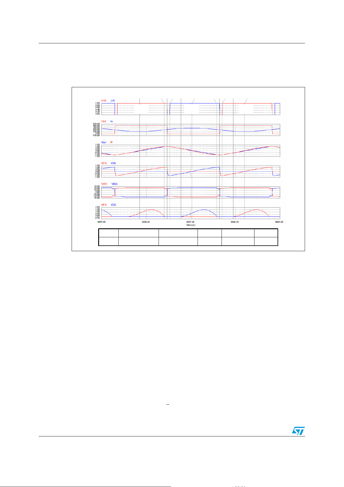
The LLC resonant half-bridge converter AN2644
soft turn-on. They cease to conduct before the transitions of the half-bridge. The
operation is DCM, then ZCS occurs by definition.
Figure 19. Operation above resonance (f > f
operation at light load
t0t
0
Q1 ON
Q2 OFF
t1t1t3t
t4t
t2t
4
2
3
Q1 OFF
Q2 ON
): main waveforms in DCMAB
R1
t5t
5
t6t6t8t8t9t
t7t
7
t10t
9
10
Q1 ON
Q2 OFF
I(D1) = D1 currentV(D1) = D1 anode voltageI(Q1) = Q1 currentIR = Tank circuit’s currentVHB = Node HB voltageHVG= Q1 gate
I(D1) = D1 currentV(D1) = D1 anode voltageI(Q1) = Q1 currentIR = Tank circuit’s currentVHB = Node HB voltageHVG= Q1 gate
I(D2) = D2 currentV(D2) = D2 anode voltageI(Q2) = Q2 currentI(Lp) = Lp (magnetizing) currentVc = Resonant capacitor voltageLVG = Q2 gate
I(D2) = D2 currentV(D2) = D2 anode voltageI(Q2) = Q2 currentI(Lp) = Lp (magnetizing) currentVc = Resonant capacitor voltageLVG = Q2 gate
2.3.3 Operation below resonance (fR2 < f < fR1, R>R
In this operating mode the converter still exhibits its usual frequency vs. load characteristic.
We will consider two submodes where, in a closed-loop regulated system, DCM operation
gets deeper and deeper as the output load is increased and frequency is moved away from
resonance.
DCMAB at medium-light load
This "below-resonance" DCM submode is exactly equal to the above-resonance DCMAB
submode previously considered. The waveforms are shown in Figure 20 and it is possible to
see that they match those shown in Figure 19.
Note only that in this case the condition I
power level than in the case of the above-resonance DCMAB submode (2:1 in the example
shown).
DCMB at heavy load
This "below-resonance" DCM submode, which is unique to below resonance operation,
actually comprises two submodes (DCMB2 & DCMB1) as frequency goes away from
resonance. Their waveforms do not differ much, only those of DCMB2 will be shown. It is
possible to identify eight fundamentals
= I(Lp) at t=t1 occurs at a considerably higher
R
subintervals and the relevant waveforms are
crit
)
30/64
Page 31
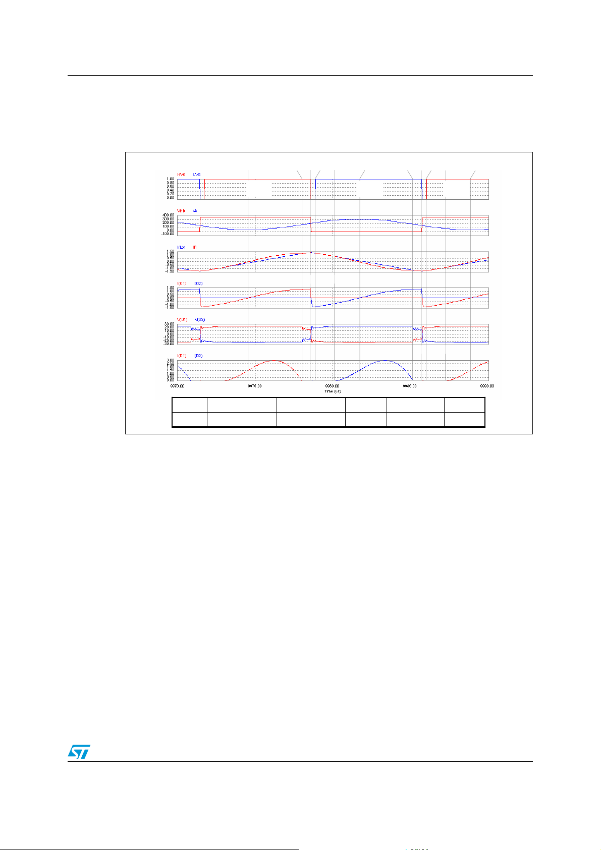
AN2644 The LLC resonant half-bridge converter
illustrated in the timing diagram of Figure 21. Again, t0 is the instant when, with Q1
conducting and Q2 open, the tank current I
has a positive-going zero-crossing.
R
Figure 20. Operation below resonance (f
DCMAB operation
t
t0t
0
0
Q2 OFF
Q2 OFF
Q1 ON
Q1 ON
t
t2t
t
t1t
2
2
1
1
< f < fR1 , R>R
R2
t
t4t
t
t3t
3
3
t
t5t
4
4
5
5
Q1 OFF
Q1 OFF
Q2 ON
Q2 ON
): main waveforms in
crit
t
t8t
t
t6t
t8t8t9t
t7t
6
7
6
7
9
9
Q1 ON
Q1 ON
Q2 OFF
Q2 OFF
I(D1) = D1 currentV(D1) = D1 anode voltageI(Q1) = Q1 currentIR = Tank circuit’s currentVHB = Node HB voltageHVG= Q1 gate
I(D1) = D1 currentV(D1) = D1 anode voltageI(Q1) = Q1 currentIR = Tank circuit’s currentVHB = Node HB voltageHVG= Q1 gate
I(D1) = D1 currentV(D1) = D1 anode voltageI(Q1) = Q1 currentIR = Tank circuit’s currentVHB = Node HB voltageHVG= Q1 gate
I(D2) = D2 currentV(D2) = D2 anode voltageI(Q2) = Q2 currentI(Lp) = Lp (magnetizing) currentVc = Resonant capacitor voltageLVG = Q2 gate
I(D2) = D2 currentV(D2) = D2 anode voltageI(Q2) = Q2 currentI(Lp) = Lp (magnetizing) currentVc = Resonant capacitor voltageLVG = Q2 gate
I(D2) = D2 currentV(D2) = D2 anode voltageI(Q2) = Q2 currentI(Lp) = Lp (magnetizing) currentVc = Resonant capacitor voltageLVG = Q2 gate
t
t10t
10
10
→ t1. Q1 is ON and Q2 is OFF. This is the "energy taking" phase, when current
a) t
0
flows from the input source to the tank circuit, so that energy is positive. The
operating point of Q1 is in the first quadrant (current is flowing from drain to
source). D2 is nonconducting and its reverse voltage is approximately 2·V
the contribution from L
voltage across Lp is a V
resonating with Ls only. I
During this phase, which ends when I
, here not shown). D1 is conducting as well, so the
L2
. Lp, then, is not participating in resonance and Cr is
out
is a portion of a sinusoid having a frequency f = fR1.
R
equals I(Lp) and, then, I(D1)=0 at t=t1, IR
R
reaches its maximum value, after that it starts decaying.
b) t
→ t2. Q1 is ON and Q2 is OFF. At t=t1 I(D1) becomes zero and IR equals I(Lp),
1
that is before the conduction time of Q2 ends. Both D1 and D2 are nonconducting
and Lp, no longer shunted by the load reflected to the primary side, goes
effectively in series to Ls and participates to resonance. I
sinusoid having a frequency f = f
. Depending on the tank circuit's parameters
R2
is a portion of a
R
and on the operating conditions, this portion can be similar to a straight line, as
shown in the diagrams of Figure 21. This phase ends when Q1 is switched off at
t=t
.
2
c) t
→ t3. This is the deadtime during which both Q1 and Q2 are OFF. At t=t2
2
I(Q1)=I(Lp)=I
swing from V
allows I
is greater than zero and provides the energy to let the node HB
R
to ground, so that the body diode of Q2, DQ2, is injected. This
in
to flow. The voltage across Lp reverses to -a·V
R
. D2 starts conducting
out
while D1 is reverse biased with a negative voltage approximately equal to 2·V
out
(plus
out
31/64
Page 32

The LLC resonant half-bridge converter AN2644
(plus the contribution from LL2, not shown here). This phase ends when Q2 is
switched on at t=t
d) t
→ t4. Q1 is OFF and Q2 is ON. At t=t3 IR is diverted from DQ2 to the R
3
.
3
of
DS(on)
Q2, so that no significant energy is lost during the turn-on transient. Note that now
the operating point of Q2 is in the third quadrant, current is flowing from the source
to drain. D2 keeps on conducting and the voltage across Lp is -a·V
is not participating in resonance and Cr is resonating with Ls only. I
a sinusoid having a frequency f = f
. This phase ends when IR=0 at t=t4.
R1
, so that Lp
out
is a portion of
R
Figure 21. Operation below resonance (f
DCMB2 operation
t
t
t0t
0
0
0
Q1 ON
Q1 ON
Q1 ON
Q2 OFF
Q2 OFF
Q2 OFF
t
t
t2t
t
t3t
t
t3t
t1t
t3t3t4t
2
2
2
1
1
1
< f < fR1, R>R
R2
4
4
4
Q1 OFF
Q1 OFF
Q1 OFF
Q2 ON
Q2 ON
Q2 ON
): main waveforms in
crit
t
t7t
t
t5t
5
5
5
t
t7t
t
t7t7t6t
t8t
6
8
6
8
6
8
Q1 ON
Q1 ON
Q1 ON
Q2 OFF
Q2 OFF
Q2 OFF
I(D1) = D1 currentV(D1) = D1 anode voltageI(Q1) = Q1 currentIR = Tank circuit’s currentVHB = Node HB voltageHVG= Q1 gate
I(D1) = D1 currentV(D1) = D1 anode voltageI(Q1) = Q1 currentIR = Tank circuit’s currentVHB = Node HB voltageHVG= Q1 gate
I(D1) = D1 currentV(D1) = D1 anode voltageI(Q1) = Q1 currentIR = Tank circuit’s currentVHB = Node HB voltageHVG= Q1 gate
I(D1) = D1 currentV(D1) = D1 anode voltageI(Q1) = Q1 currentIR = Tank circuit’s currentVHB = Node HB voltageHVG= Q1 gate
I(D2) = D2 currentV(D2) = D2 anode voltageI(Q2) = Q2 currentI(Lp) = Lp (magnetizing) currentVc = Resonant capacitor voltageLVG = Q2 gate
I(D2) = D2 currentV(D2) = D2 anode voltageI(Q2) = Q2 currentI(Lp) = Lp (magnetizing) currentVc = Resonant capacitor voltageLVG = Q2 gate
I(D2) = D2 currentV(D2) = D2 anode voltageI(Q2) = Q2 currentI(Lp) = Lp (magnetizing) currentVc = Resonant capacitor voltageLVG = Q2 gate
I(D2) = D2 currentV(D2) = D2 anode voltageI(Q2) = Q2 currentI(Lp) = Lp (magnetizing) currentVc = Resonant capacitor voltageLVG = Q2 gate
→ t5. Q1 is OFF and Q2 is ON. The tank circuit current, which is zero at t=t4
e) t
4
becomes negative. D1 is nonconducting and its reverse voltage is approximately
2·V
(plus the contribution from LL2, here not shown). Lp's current has a
out
negative slope, so the voltage across Lp must be negative. Since the diode D2 is
conducting this voltage will be equal to -a·V
resonance, Cr is resonating with Ls only and I
frequency f = f
thereby, I(D2) is zero at t=t
. During this phase, which ends when IR equals I(Lp) and,
R1
15. IR
increasing.
f) t
→ t6. This phase mirrors (t1, t2). At t=t5 I(D2) becomes zero and IR equals I(Lp),
5
that is before the conduction time of Q1 ends. Both D1 and D2 are nonconducting
and Lp, no longer shunted by the load reflected to the primary side, goes
effectively in series to Ls and participates to resonance. I
sinusoid having a frequency f = f
t=t
.
6
32/64
. Lp, then, is not participating in
out
is a portion of a sinusoid having a
R
reaches its minimum value, after that it starts
is now a portion of a
. This phase ends when Q2 is switched off at
R2
R
Page 33

AN2644 The LLC resonant half-bridge converter
g) t6 → t7. This is the deadtime during which both Q1 and Q2 are OFF. At t=t6
I
= I(Lp) is (in absolute value) greater than zero and provides the energy to let the
R
node HB swing from 0 to V
allows I
V
out
to flow back to the input source. The voltage across Lp reverses to a
R
, D1 starts conducting while D2 is reverse biased with a negative voltage
approximately equal to 2·V
This phase ends when Q1 is switched on at t=t
h) t
→ t8. Q1 is ON and Q2 is OFF. At t=t7 IR is diverted from DQ1 to the R
7
, so that the body diode of Q1, DQ1, is injected. This
in
(plus the contribution from LL2, here not shown).
out
.
7
DS(on)
of
Q1, so that no significant energy is lost during the turn-on transient. Note that now
the operating point of Q1 is in the third quadrant, current is flowing from the source
to drain. This phase, along with the preceding one is the "external energy
recirculation phase": current is negative (coming out of the input terminal) despite
that the impressed voltage is positive so that the input energy is negative, i.e. it is
returned to the input source. D1 is still conducting and the voltage across Lp is a
V
, so that Lp is not participating in resonance anymore and Cr is resonating with
out
Ls only. I
ends when I
is again a portion of a sinusoid having a frequency f = fR1. This phase
R
=0 at t=t8 and another switching cycle begins.
R
Remarks
1. Also in this "below-resonance" DCM submode the multiresonant nature of the LLC
converter shows up. From t
open and the second resonance frequency f
advantages of the LLC resonant converter over the traditional LC series-resonant
converter. In fact it helps keep operation away from capacitive mode. Although the tank
circuit current I
lags the impressed voltage (being R>R
R
have the same sign at half-bridge leg transitions, the switching period is longer than the
resonant period,1/f
. Then IR, which is decaying (in absolute value), might come close
R1
to zero or even reverse if it still evolved according to the same sinusoid at frequency
f=f
(see the extrapolated black lines drawn in (t1, t2) and (t5, t6)). This lower frequency
R1
sinusoid "holds up" the tank current, hence ensuring that the switched currents I
and I
) do not change sign and have amplitude large enough to complete the HB
R(t6
node swing well within the deadtimes (t
2. In the series LC tank Ls-Cr operating below resonance with R>R
across the L-C series is negative (the capacitive reactance is larger in module than the
inductive reactance), i.e. a minus sign is located at the node HB. As a result:
to t2 and from t5 to t6 the secondary rectifiers are both
1
2
appears. This is one of the fundamental
R2
by assumption) so that they
crit
, t3) and (t6, t7) respectively, i.e. ZVS.
the voltage drop
crit
R(t2
)
Equation 14
V
in
------- -
out
>⋅
2
aV
Then, when operating below resonance, for a given input voltage, the LLC resonant
half-bridge will provide an output voltage higher than that available at resonance, and
vice versa, with a given output voltage the LLC resonant half-bridge will operate below
a resonance if the input voltage is lower than 2·V
. In other words, the conversion
out
ratio, intended as previously mentioned, is > 1, then the LLC is said to have a "step-up"
characteristic when operating below resonance.
3. The secondary rectifiers D1 and D2 start conducting when Q2 and Q1 are switched off,
respectively. The initial current is zero and its di/dt is low, thus they have a soft turn-on.
33/64
Page 34

The LLC resonant half-bridge converter AN2644
They cease to conduct before the transitions of the half-bridge. The operation is DCM,
then ZCS occurs by definition.
4. Essentially, the reason why D2 does not conduct during (t
(t
, t6) is that during these subintervals the condition expressed by Equation 12 is met.
5
5. The waveforms in DCMB1 are very similar, only the portion of sinusoid at f = f
to zero more quickly. While DCMB2 is characterized by the duration of the intervals (t
t
) and (t5, t6) that gets longer as frequency is reduced, in DCMB1 the duration of these
2
, t2) and D1 does not during
1
decays
R2
1
intervals starts decreasing quite rapidly to reach zero at the boundary with capacitive
mode operation. The "border belt" adjacent to the capacitive region is included in the
region where DCMB1 occurs, thus it can be a good design practice to limit the
operation of the converter to the DCMB1-DCMB2 boundary.
,
2.3.4 Capacitive-mode operation below resonance (fR2 < f < fR1, R<R
In this operating mode, unique to below-resonance operation and corresponding to the
CCMB operating mode defined in [3], it is possible to distinguish six fundamental time
subintervals within a switching cycle, as illustrated in the timing diagrams of Figure 22.
In this case it is convenient to define t
a) t
→ t1. The tank current IR(t0) as Q1 is switched on is already positive: this
0
means that in the just finished deadtime it was flowing through the body diode of
Q2, DQ2. Actually, this is confirmed by the voltage V
which was previously zero and is abruptly pulled up to V
large dv/dt. The body diode DQ2 is then reverse-recovered and a large current
spike flows through Q1 and DQ2 until the latter recovers completely. Functionally
this is similar to a cross-conduction of the half-bridge leg. Very high di/dt may
occur and, as a result, large voltage spikes are generated across the parasitic
inductances experiencing this large di/dt. The voltage V
positive overshoots. During this phase when energy is taken from the input source,
the tank current reaches its maximum value and then decays. The phase ends
b) t
when I
1
=I(Lp) and, then, I(D1)=0 at t=t1.
R
→ t2. Unlike what happens in the below-resonance DCMB2 submode, where
there was insufficient voltage across the resonant capacitor to forward-bias D2,
here Vc is much larger and D2 starts conducting immediately at t=t
decreasing, becoming lower than I(Lp) and eventually crosses zero before Q1
turns off, which marks the end of the this phase at t=t
c) t
→ t3. This is the deadtime during which both Q1 and Q2 are OFF. During this
2
phase I
is already negative and further decreasing. Since Q1 is off, it is flowing
R
through DQ1. Note that the voltage of the half-bridge midpoint V
change. This phase ends when Q2 turns on at t=t
as the instant when Q1 is switched on.
0
of the half-bridge midpoint
HB
exactly at t=t0 with a
in
may have large
HB
.
2
.
3
HB
. IR starts
1
does not
crit
)
34/64
Page 35

AN2644 The LLC resonant half-bridge converter
Figure 22. Capacitive mode operation below resonance (fR2 < f < fR1, R<R
waveforms
t0t
0
Q1 ON
Q2 OFF
t1t
1
t2t
t3t
2
3
Q1 OFF
Q2 ON
t4t
t5t5t
4
I(D1) = D1 currentV(D1) = D1 anode voltageI(Q1) = Q1 currentIR = Tank circuit’s currentVHB = Node HB voltageHVG= Q1 gate
I(D1) = D1 currentV(D1) = D1 anode voltageI(Q1) = Q1 currentIR = Tank circuit’s currentVHB = Node HB voltageHVG= Q1 gate
I(D2) = D2 currentV(D2) = D2 anode voltageI(Q2) = Q2 currentI(Lp) = Lp (magnetizing) currentVc = Resonant capacitor voltageLVG = Q2 gate
I(D2) = D2 currentV(D2) = D2 anode voltageI(Q2) = Q2 currentI(Lp) = Lp (magnetizing) currentVc = Resonant capacitor voltageLVG = Q2 gate
crit
6
): main
d) t
→ t4. The tank current IR(t3) as Q2 is switched on is already negative and
3
flowing through the body diode of Q1, DQ1. The voltage of the half-bridge
midpoint, V
, is abruptly pulled down to ground at t=t3 with a large dv/dt. The
HB
body diode DQ1 is then reverse-recovered and a large current spike flows through
Q2 and DQ1 until the latter recovers completely. Again there is a condition
functionally equivalent to a cross-conduction of the half-bridge leg. Very high di/dt
may occur and, as a result, large voltage spikes are generated across the parasitic
inductances experiencing this large di/dt. The voltage V
may have large
HB
negative undershoots. During this phase energy is internally recirculated, the tank
current reaches its minimum value and then increases. The phase ends when
I
=I(Lp) and, then, I(D2)=0 at t=t4.
R
e) t
→ t5. This phase mirrors exactly (t1, t2). The voltage across the resonant
4
capacitor is so large that D1 is forward-biased and, thereby, starts conducting
immediately at t=t
. IR starts increasing, becoming higher than I(Lp) and
4
eventually crosses zero before Q2 turns off, which marks the end of this phase at
t=t
.
5
f) t
→ t6. This is the deadtime during which both Q1 and Q2 are OFF. During this
5
phase I
DQ2. Note again that the voltage of the half-bridge midpoint V
change. This phase ends when Q2 turns on at t=t
is already positive and increasing. Since Q2 is off, it is flowing through
R
and another switching cycle
3
does not
HB
begins.
35/64
Page 36

The LLC resonant half-bridge converter AN2644
Remarks
1. In the below-resonance capacitive mode operation, since current is continuously
flowing on the secondary side, this is a CCM mode (as already stated, it corresponds to
the CCMB mode defined in [3].
2. The physical reason of this CCMB operation is, as previously pointed out, the large
voltage developed across the resonant capacitor. A large energy level must be
circulating in the tank circuit and this is consistent with R<R
capacitive mode to take place. Capacitive operating mode is then likely to occur under
heavy load, overload or short circuit conditions and appropriate countermeasures must
be taken to handle this.
3. Note that in all the inductive modes the absolute value of the switched currents (i.e. the
current I
when either power MOSFET is switched off) is always greater than (in CCM
R
mode above resonance) or equal to (in all DCM modes) the current I(Lp). In the
capacitive mode, instead, the absolute value of the switched currents is lower than that
in Lp. This consideration is useful when analyzing the transitions of the node HB.
4. Unlike the other modes, in capacitive mode the secondary rectifiers D1 and D2 start
conducting during the conduction period of Q2 and Q1, respectively. The initial current
is zero and its di/dt is low, thus they have a soft turn-on. Also in this case the voltage
across the secondary rectifiers reverses as a result of their currents going to zero.
Then, ZCS is maintained even under these conditions and it is possible to conclude
that the secondary rectifiers are soft-switched at both turn-on and turn-off under all
operating conditions and that this property is inherent in the topology. In fact no
assumption has been made about the tank circuit's parameters.
condition in order for the
crit
Figure 23. No-load operation (cutoff): main waveforms
t
t0t
0
0
Q1 ON
Q1 ON
Q2 OFF
Q2 OFF
t1t
t1t1t2t
t
Q1 OFF
Q1 OFF
Q2 ON
Q2 ON
t3t
3
3
2
2
t
t4t
4
4
t
t5t
5
5
Q1 ON
Q1 ON
Q2 OFF
Q2 OFF
t
t6t
6
6
I(D1) = D1 currentV(D1) = D1 anode voltageI(Q1) = Q1 currentIR = Tank circuit’s currentVHB = Node HB voltageHVG= Q1 gate
I(D1) = D1 currentV(D1) = D1 anode voltageI(Q1) = Q1 currentIR = Tank circuit’s currentVHB = Node HB voltageHVG= Q1 gate
I(D1) = D1 currentV(D1) = D1 anode voltageI(Q1) = Q1 currentIR = Tank circuit’s currentVHB = Node HB voltageHVG= Q1 gate
I(D2) = D2 currentV(D2) = D2 anode voltageI(Q2) = Q2 currentI(Lp) = Lp (magnetizing) currentVc = Resonant capacitor voltageLVG = Q2 gate
I(D2) = D2 currentV(D2) = D2 anode voltageI(Q2) = Q2 currentI(Lp) = Lp (magnetizing) currentVc = Resonant capacitor voltageLVG = Q2 gate
I(D2) = D2 currentV(D2) = D2 anode voltageI(Q2) = Q2 currentI(Lp) = Lp (magnetizing) currentVc = Resonant capacitor voltageLVG = Q2 gate
36/64
Page 37

AN2644 The LLC resonant half-bridge converter
2.4 No-load operation
The ability to operate under no-load conditions is another peculiar characteristic of the LLC
resonant half-bridge converter. The typical waveforms in this operating mode, called also
"cutoff" mode, which can occur at frequencies both above, below and at the resonant
frequency f
Note that it is I
by portions of sinusoid at f=f
this operation to occur, the voltage developed across Lp and reflected to the secondary side
has to be lower than the output voltage throughout the entire switching cycle, so that either
secondary rectifier cannot be forward-biased. In other words, Equation 12 has to be met for
t ∈(t
, t6). The ability of the converter to operate with no-load can be easily deducted by
0
Equation 12 itself. However big the peak value of V
zero, it is possible to find a value of Lp that meets condition (α). In the end, no-load
operation is not an intrinsic property of the LLC resonant converter (like ZCS for the
secondary rectifiers) but it can be achieved with an appropriate design of the tank circuit.
, as demonstrated in [3], are illustrated in the timing diagrams of Figure 23.
R1
=I(Lp), then I(D1)=I(D2)=0, throughout the entire switching cycle. IR is made
R
, but looks very much like a triangular waveform. In order for
R2
(t)-Vc(t) is and provided a·V
in
out
is not
The difference with respect to the LC series resonant converter is apparent. If Lp →
∞ the
LLC converter turns into the LC one but Vc → 0 because there is no current through the
resonant tank and the only possible equilibrium condition is V
= a·V
in
. If the input and
out
output voltage have a different ratio, output voltage regulation will be impossible.
Seen from a different standpoint, under no load conditions and at a frequency considerably
higher than f
, the resonant capacitor Cr "disappears" (Vc(t) ≈ Vin/2) and the output voltage
R1
is given by the inductive divider made up by Ls and Lp as shown by the equivalent circuit of
Figure 24. Then, if the voltage conversion ratio is greater than the inductive divider ratio,
regulation will be possible at some finite frequency, otherwise it will not be. From Equation
12, substituting V
= Vin and, then, Vc(t) = Vin/2, it is possible to find a necessary condition
in(t)
in order for the converter to be able to regulate at zero load:
Equation 15
aV
≤
⋅
------------------ -
2
V
out
in
Lp
------------------- -
Ls Lp+
Lp, then, plays a key role. It not only makes zero load operation possible but allows softswitching under these conditions too, as already discussed. The price to pay for that is the
considerable tank current I
=I(Lp) circulating in the circuit and illustrated in Figure 23. This
R
circulation is not lossless. Power is dissipated in power MOSFET, the resonant capacitor
and the transformer.
This prevents the LLC resonant converter from achieving extremely low input power levels at
no load, unless appropriate countermeasures are taken. The most effective way to reduce
no-load consumption to a very low level is to let the converter operate intermittently ("burstmode" or "pulse-skipping" operation). In this way, the average value of the tank current can
be reduced at an almost negligible value. Furthermore, the average switching frequency will
be considerably lowered thus minimizing the residual turn-off switching losses.
2.5 Overload and short circuit operation
The equivalent schematic of the converter under short circuit conditions is illustrated in
Figure 25. The inductance Lp is actually shunted by an extremely low impedance, so that
the LLC circuit reduces to a series LC circuit. The transformer will work as a "current
transformer", so that the output current will be a times the primary (input) current Iin. It is
37/64
Page 38

The LLC resonant half-bridge converter AN2644
intuitive that the impedance of the Ls-Cr resonant tank plays a key role. Note that this
impedance becomes zero at f = f
. Two cases will be considered:
R1
1. The converter always works above resonance (some means is provided to bottom-limit
the operating frequency at a value f
output voltage regulated, will reduce the switching frequency to the minimum value f
> fR1). The control loop, in the attempt to keep the
m
m
In this case the converter still operates in the inductive region (CCM submode) and
ZVS is ensured. However, the impedance of the Ls-Cr tank circuit can be very low and
then the current Iin can reach very high values, the closer the minimum frequency to
f
is, the lower the impedance and the higher the current will be.
R1
2. The converter can operate below resonance (some means is provided to bottom-limit
the operating frequency at a value f
such that fR2 < fm < fR1). Again, the control loop,
m
in the attempt to keep the output voltage regulated, will reduce the switching frequency
to the minimum value f
of the Ls-Cr tank circuit at a value that is as lower as f
. In this case, the input current will be limited by the impedance
m
is lower. However the capacitive
m
region is entered and ZVS is lost, with all the consequent troubles previously
mentioned. The waveforms will be similar to those in Figure 22.
.
Figure 24. Circuit's equivalent schematic
under: no-load conditions
Ls
Ls
Lp
Vin
VinVin
a·Vout
a·Vouta·Vout
Lp
a:1
a:1
Vout
VoutVout
It is interesting to see what happens under short circuit if the converter is operating at
resonance (f = f
). Tank circuit's impedance is zero, then the short circuit is directly
R1
connected across the input source and the current Iin is theoretically unlimited.
Theoretically, switching frequency should not change (the system is working in the loadindependent point). In real-world operation, Iin, though reaching very high values, will be
limited by the parasitic resistance of the short-circuit mesh, the ESR of Cr and by
transformer's nonidealities. Additionally, the drop across the secondary rectifiers does not
reflect a true short circuit on the primary side. Because of the parasitic resistances, the
output voltage will drop and the control loop will react pushing the operating frequency to the
minimum f
, which, realistically, must be lower than fR1 if operation at resonance is allowed.
m
In the end this will fall into case 2.
Figure 25. Circuit's equivalent schematic
under: short-circuit conditions
Iin
Iin
Cr Ls
Cr Ls
Vin
Vin
Still with reference to case 2, it is worth remembering that the capacitive region is entered
and ZVS for MOSFETs is lost as , well before short circuit.
R
crit
From the above analysis it is possible to draw the following conclusions:
1. Two major issues arise under overload or short circuit conditions: very high current
levels, and capacitive mode operation (with loss of ZVS, etc.). This makes the operation
of the LLC resonant converter under overload or short circuit inherently unsafe if no
overcurrent protection (OCP) is used, just like in conventional PWM-controlled
converters. OCP will have to prevent not only the tank current from exceeding unsafe
38/64
Zo0Zo∞⋅=
Page 39

AN2644 The LLC resonant half-bridge converter
values but also ZVS from being lost. In principle, its setpoint must be such that the
condition R>R
is always fulfilled.
crit
2. Limiting the minimum operating frequency of the converter is not always effective. It
prevents losing ZVS under overload or short circuit only if this minimum value is above
the resonant frequency f
. Thereby, relying on just limiting the minimum operating
R1
frequency would force giving up the below-resonance operating region and its
interesting properties, severely limiting the usability range of the converter.
Furthermore, the problem of having too high circulating current would be still unsolved.
3. Converters are often specified to have peak load demands that are considerably higher
than the maximum continuous power, and whose duration is such that it cannot be
averaged by the output capacitor bank. While these peak loads may be thermally
irrelevant, from the electrical standpoint they must be considered as steady-state. OCP
circuits must not be triggered and the converter must be designed so that the condition
R>R
is not violated under these transient conditions as well.
crit
The inspection of the waveforms under heavy load conditions shows that, unlike PWMcontrolled converters, the peak current in a switching cycle is not reached at the end of the
conduction time of either MOSFET. This suggests that the usual cycle-by-cycle current
limitation so widely used in PWM-controlled converters is not applicable to LLC resonant
converters.
The simplest and also most immediate action to take in response to the detection of an
overload or short circuit condition is to increase the operating frequency. It is advantageous
to push the frequency well above the resonance frequency f
, so that the converter
R1
definitely operates in the inductive region, and ZVS is maintained, with the input current kept
under control by the inductive reactance of the tank circuit.
However, this frequency rise is not typically sufficient to effectively limit the short-circuit
output current at safe values. In fact, on one hand, the input impedance of the tank circuit in
the inductive region is essentially proportional to frequency. Since there are practical limits
on the maximum operating frequency (it rarely exceeds 3-4 times f
current can still be considerably large. On the other hand, as the output voltage drops
because of the action of the OCP circuits, the voltage reflected across Lp becomes smaller
and smaller. Then, less and less current flows through Lp and the transformer tends to
transfer all the primary current to the output.
As a consequence, the short circuit output current can be still much higher than the nominal
full-load current and the resulting stress, especially for the secondary rectifiers, might be
unacceptable. In addition to current limiting it is therefore advisable to provide some timed
shutdown protection that either forces an intermittent operation of the converter to
drastically reduce the average value of the output current or latches it off if the OCP circuits
are active for more than some time.
2.6 Converter's startup
Like in PWM-controlled converters, startup is quite a critical moment that needs to be
properly handled in LLC resonant converter as well. When the converter is first switched on
(or also while it is recovering after a protection shutdown) the energy flow should be
progressively increased to allow a slow buildup in output current and voltage. This is
commonly known as "soft-start". Doing otherwise, high and potentially destructive currents
might be drawn from the input source and through the power devices in an attempt to
charge the output capacitors and bring the output voltage to the regulated value.
), the short circuit tank
R1
39/64
Page 40

The LLC resonant half-bridge converter AN2644
Since at startup the output capacitors are discharged, the startup phase can be regarded as
a "temporary short circuit" (where, however, the output voltage is allowed to increase) and
actually it has to be handled like a short circuit as mentioned in the previous section. To
minimize energy flow, the initial switching frequency will have to be much higher than the
resonance frequency f
, so that the converter operates in the inductive region, ZVS is
R1
maintained and the input current is kept under control by the inductive reactance of the tank
circuit. The frequency will be allowed to progressively decay until the output voltage comes
close to the regulated value and the control loop closes and takes over.
Some typical waveforms at startup for the converter of Figure 15 are shown in Figure 26,
where the initial frequency is set at 300 kHz (against f
≈ 76 kHz).
R1
In the LLC resonant converter there is an additional phenomenon that shows up just at the
very beginning and causes higher resonant tank current to flow and ZVS loss.
As mentioned in the Section 2, the resonant capacitor Cr plays the double role of resonant
capacitor and DC blocking capacitor. This essentially means that the resonant voltage on Cr
is superimposed on a DC value that equals V
duty cycle. As a result, the primary of the transformer is symmetrically driven by a ±V
/2 because the half-bridge is driven with 50%
in
/2
in
square wave. This is true when steady-state operation has been reached.
At startup the initial voltage across Cr is zero and for the first few cycles the voltage seen by
the transformer when the high-side power MOSFET Q1 is on is considerably different from
the voltage seen when Q2 is on. The transformer driving voltage will tend to become
symmetrical as switching cycles follow one another and Cr is charged at the steady state
DC level. During the Cr charge transient the v·s unbalance can be quite high and this makes
the tank current irregular in the first few cycles, with peak values that can be considerably
higher than the steady-state peak-to-peak current expected at the starting frequency.
Additionally, the fundamental ZVS conditions ("when one switch turns off, the tank current
must have the same sign as the impressed voltage") may be violated so that even capacitive
mode operation can be observed.
Figure 26. Converter's startup: main waveforms
I(D1) = D1 currentV(D1) = D1 anode voltageI(Q1) = Q1 currentIR = Tank circuit’s currentVHB = Node HB voltageHVG= Q1 gate
I(D1) = D1 currentV(D1) = D1 anode voltageI(Q1) = Q1 currentIR = Tank circuit’s currentVHB = Node HB voltageHVG= Q1 gate
I(D1) = D1 currentV(D1) = D1 anode voltageI(Q1) = Q1 currentIR = Tank circuit’s currentVHB = Node HB voltageHVG= Q1 gate
I(D2) = D2 currentV(D2) = D2 anode voltageI(Q2) = Q2 currentI(Lp) = Lp (magnetizing) currentVc = Resonant capacitor voltageLVG = Q2 gate
I(D2) = D2 currentV(D2) = D2 anode voltageI(Q2) = Q2 currentI(Lp) = Lp (magnetizing) currentVc = Resonant capacitor voltageLVG = Q2 gate
I(D2) = D2 currentV(D2) = D2 anode voltageI(Q2) = Q2 currentI(Lp) = Lp (magnetizing) currentVc = Resonant capacitor voltageLVG = Q2 gate
40/64
Page 41

AN2644 The LLC resonant half-bridge converter
This phenomenon is well-known in push-pull and half-bridge topologies and is sometimes
referred to as "flux doubling" because the transformer's magnetic flux excursion, which
normally swings by 2B
goes from 0 to 2B
from -Bpk to +Bpk under steady state operation, in the first cycle
pk
. Fortunately, if the integrated magnetics approach is used, there will be
pk
no risk of saturation. Flux doubling will concern only the resonant inductor Ls, which is
mostly associated to the transformer's leakage inductance that, by definition, cannot
saturate because the relevant flux is developed in air.
Although not inherently hazardous, (capacitive mode and ZVS loss will typically occur in the
first two-three cycles, then the associated stress level is practically negligible) this
phenomenon is not nice to see. To eliminate or, at least, minimize it, the split capacitor
configuration of Figure 4 can be used in some cases. In fact, the initial voltage across each
capacitor will be close to V
/2 (equal to Vin/2 if the two capacitors had exactly the same
in
value), then there will be only a minimum transient.
However, this is ineffective with many control ICs with high-side MOSFET driving capability
using capacitive bootstrap. To guarantee an adequate precharge of the bootstrap capacitor
to correctly drive the high-side MOSFET Q1 since the first cycle, the low-side MOSFET Q2
is turned on for some time before starting to operate (as shown in Figure 26), which
discharges completely the lower Cr/2 capacitor. This bootstrap precharge mechanism,
shown in Figure 27, makes ineffective also any pull-up that could precharge Cr.
In this case the initial current peak cannot be completely eliminated, just reduced by either
using a higher starting frequency or by forcing the duty cycle to start from a value
considerably smaller than 50% and letting it widen progressively.
Figure 27. High-side driving with bootstrap approach and bootstrap capacitor
charge path
Vin
Vin
D
D
BOOT
BOOTDBOOT
I
I
I
BOOTCHARGE
BOOTCHARGE
BOOTCHARGE
Vcc
Vcc
Level
Level
Shifter
Shifter
Vcc
Vcc
Control
Control
Logic
Logic
2.7 Analysis of power losses
Conduction power losses on the primary side are located in the power MOSFETs, in the
resonant capacitor Cr and the transformer (for convenience the secondary winding losses
can be incorporated). On the secondary side, losses will be essentially located in the
secondary rectifiers, although those in the output capacitors cannot be neglected, at least
as far as capacitor selection is concerned.
C
C
BOOT
BOOTCBOOT
Q1
Q1
Q2
Q2
Ls
Ls
a:1:1
a:1:1
Lp
Lp
Cr / 2
Cr / 2
Cr / 2
Cr / 2
41/64
Page 42

The LLC resonant half-bridge converter AN2644
⎧⎫
Unless the converter is running at very high frequency, which would make turn-off losses
dominant, R
is usually the major source of power loss in power MOSFET. In the total
DS(on)
loss budget, however, the power wasted in power MOSFETs is usually a minor contributor,
especially when the converter is powered from the output of a PFC preregulator (400 V
typ.). It is not uncommon to see power MOSFETs running cool with minimum heat sinking.
The resonant capacitor Cr dissipates because of its own ESR. For this reason, especially
when very high efficiency is required, Cr should be a low-loss one, suited for AC/pulse
applications. Polypropylene film capacitors are the preferred choice.
Concerning the transformer, high frequency copper losses need to be particularly
addressed. In fact, eddy currents and proximity losses are considerable, especially in the
side-by-side winding arrangement because of the high transverse flux. Litz-type or
multistrand wire is a must for both primary and secondary windings.
Switching losses are essentially located in the power MOSFET Q1 and Q2. As previously
stated, the value of the switched current at heavy load (I
) is a trade-off between the
Rmin
need for ensuring ZVS for both Q1 and Q2 and their turn-off losses. The higher the
switched current is, the higher the margin for ZVS will be, but at the expense of larger
switching loss due to voltage-current overlap. It is intuitive that the optimum design, in terms
of total dynamic losses minimization, is the one that uses for I
the minimum value
Rmin
necessary to achieve ZVS. It still provides zero capacitive turn-on losses with minimum
switching losses at turnoff. Since component tolerance must be accounted for, and losing
ZVS must be avoided not only for efficiency reasons but also to prevent troubles, adequate
margin needs to be considered and the typical operation will be suboptimal.
Secondary rectifiers are usually the components where the majority of power losses occur.
Assuming the rectifiers are identical, their cumulative conduction losses are given by:
Equation 16
V
⎪⎪
thIout dc–
=
⎨⎬
⎪⎪
2V
⎩⎭
where V
Pd
is the rectifier's threshold voltage and Rd its dynamic resistance. With bridge
th
rectification, losses are almost double because there are always two diodes in the
conduction path (we say "almost" because of the lower blocking voltage rating, so that V
and R
are expected to be slightly lower for the same current rating). Hence this
d
arrangement is preferred when the output voltage is high. Firstly, the efficiency loss due to
the rectifiers (which is ∝ 2 V
F/Vout
output voltage is, the more a lower blocking voltage requirement becomes beneficial.
As compared to the ZVS Asymmetrical Half-bridge and the Forward converter, conduction
losses (for the same technology and blocking voltage) would be slightly greater because of
the worse current form factor that would increase the term, but this is compensated by the
absence of recovery and its associated losses. In the end, considering also that in the LLC
resonant half-bridge there is no secondary choke with its associated losses, it is expected
that the total secondary losses will be lower.
2.8 Small-signal behavior
thIout dc–
2
RdI
+
out rms–
2
RdI
+()
out rms–
full - wave rectification
bridge rectification
) becomes less significant. Secondly, the higher the
th
It is essential to know the small-signal behavior of the LLC resonant converter to be able to
design the feedback loop. In line with the approach followed to describe its steady-state
42/64
Page 43

AN2644 The LLC resonant half-bridge converter
operation, here only a qualitative description will be given, which is the result of a
characterization by simulation [7] (refer to Section 4).
As stated many times, the operating frequency is the parameter that allows regulation of the
input-to-output energy flow. The control-to-output transfer function G(j
ω) that characterizes
the small-signal behavior of the LLC resonant converter will then be defined as:
Equation 17
^
V
o
------ Gjω()=
^
f
In the overall converter's dynamics it is convenient to separate the contribution of the
"inverter" part and that of the rectifying and filtering block that transforms the inverter in a
converter. This is quite a useful concept of superposition because it gives considerable
physical insight. Regardless of the operating mode of the inverter and, then, of its
contribution to converter's dynamics, the rectifying and filtering block always introduces a
low frequency pole associated to the output capacitor, the load resistance and the openloop output impedance Zo
of the resonant tank, plus a zero due to the output capacitor and
0
its ESR (equivalent series resistor). This pole moves with the load (frequency is higher at
heavy load, lower at light load) because of the changes in Zo
essentially fixed frequency, exactly like in PWM converters.
Different types of dynamic behavior, corresponding to different pole distributions of G(j
can be observed depending on the operating mode. Again we will consider operation at,
above and below resonance.
2.8.1 Operation above resonance (f > fR1)
In this operating mode the converter features a special characteristic typical of resonant
converters, the so-called "beat frequency double pole", i.e. two complex and conjugate
poles having their imaginary part at the difference between the switching frequency f and
the resonant frequency f
there is the pole-zero pair associated to the output filter. If f is significantly higher than f
the system can be regarded as a single-pole system.
. In addition to this double pole, contributed by the inverter part,
R1
, while the zero is at an
0
ω),
R1
,
As switching frequency moves close to resonant frequency, the beat frequency double pole
will move to lower frequency. When the switching frequency is very close to resonant
frequency, the beat frequency double pole will eventually split and become two real poles.
One moves to higher frequencies and the other moves to lower frequencies as switching
frequency gets closer and closer to resonant frequency. Finally, the split pole moving to low
frequency will merge with the low frequency pole caused by the output filter and form a
double pole. This type of characteristic is very similar to that of the conventional series LC
converter.
Provided the converter is not operating too close to resonance, as long as it runs in CCM,
the pole distribution tends not to change significantly. In DCM operation, instead, the beat
frequency double pole will more pronouncedly move to higher frequencies and the low
frequency pole to lower frequencies. At light load, the converter can then be regarded as a
single-pole system.
Concerning how the resonant tank characteristics affect the small-signal behavior, the
parallel inductor Lp has no practical effect. Conversely, increasing the impedance of the
resonant tank (i.e. increasing Ls and reducing Cr while keeping the same f
), the DC gain
R1
will increase. Also the low frequency pole changes with the resonant tank impedance (it
43/64
Page 44

The LLC resonant half-bridge converter AN2644
gets higher at low impedance). In fact, the low frequency pole is not determined by the load
resistor alone but by the output impedance of the tank circuit as well.
2.8.2 Operation below resonance (fR2 < f < fR1, R>R
In this operating mode the converter's dynamics changes considerably. In the left half-plane,
there are three poles and one zero but no beat frequency double pole. The pole distribution
is quite insensitive to switching frequency as compared to that in the above resonance
operation. The pole that in the above resonance operation was moving to higher frequency
when switching frequency was approaching resonance here moves back to lower
frequencies as switching frequency is further reduced going away from resonance. Its
position, however does not change much. The low-frequency double pole is minimally
affected too.
A Right Half Plane Zero (RHPZ) can be observed that moves with switching frequency but,
fortunately, it stays typically away from the low frequency region of interest in the design of
the feedback loop.
Approaching capacitive region, beat frequency dynamics tends to appear again. The phase
has an abrupt 180º shift just beyond the capacitive region threshold (feedback from negative
turns into positive).
Starting from heavy load conditions, at first the Q associated to the low frequency double
pole decreases. The RHPZ shifts to higher frequencies and leaves the stage. Further
reducing the load, the Q of the low frequency double pole increases. At very light load the
low frequency double pole splits, one moves to higher frequencies and the other to lower
frequencies. Again, at very light load the converter can be regarded as a single-pole system.
Unlike in the above resonance operation, in this case the parallel inductor Lp has a
considerable impact on the DC gain of the converter. Additionally, it affects the RHPZ as
well. Larger values for Lp tends to shift it to lower frequencies. As far as the impedance of
the resonant tank is concerned, the effect is the same as in the above resonance operation.
crit
)
2.8.3 Operation at resonance (f = fR1)
Operation at resonance can be regarded as the borderline between the two previously
considered operating modes. The behavior will not be different from that seen just above
(and just below) resonance: two low-frequency poles, one high-frequency pole and the ESR
zero. The same behavior can be seen as far as load dependence is concerned.
The compensation of the error amplifier must consider the different types of small-signal
behavior that the converter can exhibit, especially if it is designed to operate both above and
below resonance. The challenge comes essentially from its second-order behavior exhibited
in its operation close to resonance frequency due to the low frequency double pole. To
properly compensate that, the best option is a type 3 amplifier, i.e. a compensator with one
pole at the origin plus two poles and two zeros at finite frequencies. The pole at the origin
gives excellent load and line regulation characteristics. The two zeros are placed at low
frequency to compensate the double pole of the control-to-output transfer function, by
counteracting their phase lag. The poles are placed to compensate the ESR zero and
provide more attenuation at switching frequency. A practical implementation of this
compensator is shown in Figure 28 along with the relationship between the component
values and its transfer function.
44/64
Page 45

AN2644 The LLC resonant half-bridge converter
Figure 28. Frequency compensation with an isolated type 3 amplifier (3 poles + 2
zeros)
Vo
Vo
RF2
RF2
RB1
Ic
Ic
CF3
CF3
RF3
RF3
RB1
CTR
CTR
TL431
TL431
CF2
CF2
RB2
RB2
CF1
CF1
RF1
RF1
R1
R1
R2
R2
Equation 18
^
I
C
------
^
V
o
CTR
-------------------------------------------------
sR1 RB1 CF1⋅⋅()
1sRB1RF2+()CF2+
------------------------------------------------------------ -
⋅⋅=
1sRF2CF2⋅+
1 s R1 RF1+()CF1+
--------------------------------------------------------
1sRF3CF3⋅+
45/64
Page 46

Conclusion AN2644
3 Conclusion
The operation of the LLC resonant converter has been examined in detail and its most
important properties have been deduced by inspection of its salient waveforms under
different operating conditions. To summarize, the most significant merits of this topology are:
● Soft-switching of all semiconductor devices: ZVS (zero-voltage switching) at turn-on for
the MOSFETs and ZCS (zero-current switching) at both turn-on and turn-off for the
secondary rectifiers. The first property results from a correct design of the resonant
tank. The second one is a natural feature of the topology.
● Ability to accommodate an extremely broad load range, including zero load, with an
acceptable frequency variation. Also this property results from a correct design of the
resonant tank.
● Magnetic integration, which allows the combination of different magnetic devices into a
single physical device.
● Smooth waveforms: the current is piecewise sinusoidal with no steep edges. The
voltage, although a square wave, does not have very high dv/dt edges. EMI emissions
are considerably low and filtering requirements are relatively loose.
● As a result of all the above merits, high-efficiency, high switching frequency capability,
high power density are typical characteristics of the converters based on this topology.
The most significant facts concerning the design of an LLC resonant converter are:
● The quantities that determine whether the converter operates at resonance, above
resonance or below resonance are essentially the input and the output voltages and
the transformer's turn ratio. There is just a second-order dependence on the load
current due to the variation of the voltage drop across parasitic elements such as
winding resistance, rectifier drop, etc.
● Operation at resonance looks like the preferred operating point, where load regulation
is ideally zero, where tank current is maximally sinusoidal and where CCM operation
minimizes peak tank current for a given power throughput. Whenever possible (e.g.
when the LLC converter is powered by a PFC preregulator) it seems a good design
strategy to design the converter to work at resonance under nominal conditions, and
use below resonance operation to handle mains voltage dips and above resonance
operation to handle light load or transient overshoots of the input voltage.
● The ability to operate under no-load conditions and to ensure ZVS operation depend
essentially on the transformer's magnetizing inductance. Its value has to be traded off
against the switching losses at full load operation and the input consumption at no-load.
● Avoiding capacitive mode operation is a must. It is a too risky operating mode and any
design procedure should not leave this fundamental aspect out of consideration.
● Overcurrent and short circuit protection must be provided. They will not only have to
prevent excessive currents from flowing in both the resonant tank, the transformer and
the output rectifiers but also avoid entering capacitive mode operation.
● Soft-start is highly recommended. At startup there is a situation very similar to a short
circuit and, if not properly controlled, potentially destructive currents might flow in the
half-bridge leg and the resonant tank.
46/64
Page 47

AN2644 References
4 References
1. "Resonant Converter Topologies with Three and Four Energy Storage Elements", IEEE
Trans. on Power Electronics, Vol. 9, No. 1, 1994, Pages 64 - 73
2. "A Comparison of Half Bridge Resonant Converter Topologies", IEEE Trans. on Power
Electronics, 1988. Pages: 174 - 182.
3. "Steady-state Analysis of the LLC Resonant Converter", Applied Power Electronics
Conference and Exposition, 2001. APEC 2001. Pages: 728 - 735
4. "First harmonic approximation including design constraints", Telecommunications
Energy Conference, 1998. INTELEC. Pages: 321 - 328
5. "Design Optimization for an LCL-Type Series Resonant Converter",
http://www.powerpulse.net/features/techpaper.php?paperID=76
6. "Fundamentals of Power Electronics", 2
7. "Topology Investigation for Front End DC/DC Power Conversion for Distributed Power
System", PhD dissertation, Virginia Polytechnic Institute and State University, 2003.
nd
edition, Kluwer, 2001
47/64
Page 48

Power MOSFET driving energy in ZVS operation AN2644
Appendix A Power MOSFET driving energy in ZVS
operation
When power MOSFETs are switched on under ZVS conditions, i.e. when their drain-tosource is already zero, Miller effect due to drain-to-source voltage modulation is absent.
This reduces the gate charge required to turn the power MOSFET fully on, the turn-on
energy, as well as the total driving energy. This can be conveniently examined on the gatecharge characteristic of the device (see Figure 29).
Figure 29. Comparison of gate-charge characteristics with and without ZVS
The black curve is the normal piecewise-linear gate-charge curve. The first portion is that
related to the charge of the input capacitance C
bring the gate voltage up to the plateau value V
specified current. The flat portion is the so-called "Miller plateau", where the gate voltage
does not increase because the drain-to-source voltage is falling and C
charge supplied to the gate until the charge Qgd has been supplied. The third rising portion
is related to the overcharge of C
GS+CGD
this line is lower than that of the first portion. This is due to the modulation of C
now considerably larger (C
is essentially constant). The total gate charge supplied to the
GS
gate to bring its voltage up to the final value V
specified on the datasheet for given V
GS
The grey-hatched area included between the gate-charge curve and the V
is the energy lost in the gate driver to charge the gate up to the final value V
power MOSFET fully on. Its value can be found with simple geometric considerations:
Equation 19
1
-- -
E
ONHS
-
48/64
2
QgsV
GS+CGD
that lets the power MOSFET carry the
M
, and Qgs is the charge needed to
needed to minimize R
is Qg. The values of Qgs, Qgd, Qg are
GS
, VDS, ID.
Qg Qgs Qgd++()VGSVM–()+[]=
M
is wiping out the
GD
. Note that the slope of
DS(on)
horizontal line
GS
and turn the
GS
, which is
GD
Page 49

AN2644 Power MOSFET driving energy in ZVS operation
The grey-shaded area below the gate charge curve represents the energy lost in the gate
driver to discharge the gate from V
to zero. Its value can be simply found from the
GS
difference of the total driving energy, represented by the rectangle enclosed by the Q-V axes
and the Qg and V
GS
lines:
Equation 20
E
HS
Qg VGS⋅=
and E
ON_HS
:
Equation 21
E
OFFHS
-
Qg VGSE
–⋅=
ONHS
-
In case of ZVS, instead, the associated gate-charge curve is the red line. Its slope is equal
to that of the third portion of the normal gate-charge characteristic, because C
final value since the beginning. By geometrical considerations, the total gate charge Qg
has the
GD
Z
to
provide in this case will be:
Equation 22
V
GS
Z
------------------------ -
V
–
GSVM
Qg Qgs Qgd+()–[]=
and turn
GS
Qg
while the energy lost in the gate driver to charge the gate up to the final value V
the power MOSFET fully on and represented by the red-shaded area will be:
Equation 23
2
E
ONZVS
1
-- -
Qg
-
ZVGS
2
1
-- -
------------------------ -
2
V
GSVM
V
GS
Qg Qgs Qgd+()–[]⋅==
–
At turn-off, the Miller effect will be present but to a lower degree. In fact, the operating point
will initially move along the red line until the gate voltage reaches the Miller plateau V
(that
M
associated to the switched current at turn-off). From that point on, it will move along the
black curve. The energy associated to turn-off will be:
Equation 24
E
OFFZVS
-
1
--------------------------------- -
–()
2V
GSVM
2
V
GS
2
V
+()Qg Qgd–()VGSVGSVM+()Qgs–[]=
M
and the total driving energy:
Equation 25
E
1
--------------------------------- -
ZVS
2VGSVM–()
2V
2
2
V
+()Qg Qgd–()VGS2V
GS
M
+()Qgs–[]=
GSVM
For the power MOSFET used in the example of Figure 29 (STP14NK60Z), the datasheet
specifies: Qgs = 13.2 nC, Qgd = 38.6 nC, Qg = 75 nC @ V
values and V
nJ, E
OFF_HS
= 5.8 Vin (Equation 19) to (Equation 25) we find: E
M
= 445 nJ, QgZ = 55 nC, E
ON_ZVS
= 276 nJ, E
= 10 V. Substituting these
GS
ON_HS
OFF_ZVS
= 305 nJ, EHS = 750
= 331 nJ and E
ZVS
= 607
nJ. Then, the total gate charge is decreased by 20 nC (-27%) and the total gate driving
energy by 143 nJ (-19%).
49/64
Page 50

Resonant transitions of half-bridge midpoint AN2644
Appendix B Resonant transitions of half-bridge midpoint
To analyze the transitions of the half-bridge midpoint node HB when either Q1 or Q2 is
turned off, it is necessary to schematize the equivalent circuit during the transient. For
simplicity only the turn-off of Q2 will be considered, being obvious that the turn-off of Q1 will
be exactly mirror-symmetrical. Different circuits need to be considered, depending on
whether the converter is operated in a DCM mode or a CCM mode. These equivalent
circuits are shown in Figure 30.
Figure 30. Equivalent circuit to analyze the transitions of the half-bridge midpoint
node when Q2 turns off
V
V
V
Ls
Ls
Ls
a·(Vout+VF)
a·(Vout+VF)
a·(Vout+VF)
ON
ON
ON
t = 0
t = 0
t = 0
OFF
OFF
OFF
V
V
VCV
C
C
C
I
I
IRI
R
R
R
Cr CrLs Ls
Cr CrLs Ls
Cr CrLs Ls
LpC
LpC
V
V
V
V
VHBV
HB
HB
HB
HB
HB
HB
DCM operation CCM operation
DCM operation CCM operation
VLV
LpC
L
L
L
ON
ON
ON
ON
t = 0
t = 0
t = 0
t = 0
OFF
OFF
OFF
OFF
I
I
IRI
R
R
R
C
C
C
V
V
VHBV
HB
HB
HB
HB
HB
HB
V
V
VCV
C
C
C
In fact, in the case of DCM operation, since the secondary windings are open, Lp is part of
the circuit and is effectively in series to Ls to form a single inductor Ls+Lp. In CCM
operation, instead, since the secondary windings are conducting there is a constant voltage
equal to ±a·(V
) across Lp and then this can be replaced by a voltage generator
out+VF
(placed as shown in Figure 30 in the case under consideration). In either circuit, Q2 is
replaced by an ideal switch that opens at t=0.
Resonant tanks are again involved during the transitions, hence the denomination "resonant
transitions" given to the swings of the node HB. Considering the operation of the LLC
resonant converter in its entirety, then, there are four associated resonant frequencies.
C
is the total parasitic capacitance of the node HB already discussed in Section 2.2: The
HB
switching mechanism and illustrated in Figure 8 and that will be the topic of the next section.
Note that during the transient Cr and C
Cr>>C
the changes of the V
assume V
V
C
The value of V
(typically, two orders of magnitude), the combined capacitance will be ≈CHB and
HB
= VC(0) during the transient and replace Cr with a constant voltage generator
C
voltage during the transient can be neglected, so that it is possible to
C
(0).
(0) can be determined on the basis of the following considerations. The
C
value of at the end of the conduction cycle of Q1, V
are effectively in series. However, since normally
HB
(Ts/2), is given by:
C
Equation 26
Ts
⎛⎞
------ -
V
C
⎝⎠
2
50/64
Ts
------ -
1
2
V
------
0()
+=
C
Cr
∫
IRt() td
0
Page 51

AN2644 Resonant transitions of half-bridge midpoint
Note that the integral in Equation 26 is the total charge provided to Cr during the conduction
time of Q1, when the converter draws current from the input source. This charge can be
expressed also as the product of the DC input current Iin times the switching period, then:
Equation 27
V
C
Ts
⎛⎞
------ -
⎝⎠
2
V
Iin
------ -
0()
Cr
Ts+=
C
On the other hand, remembering that V
has a DC value equal to Vin/2, for symmetry the
C
following identity holds true:
Equation 28
V
V
C
Ts
⎛⎞
------ -
⎝⎠
2
------- -
2
in
V
in
------- - V
2
0()–=–
C
By combination of (Equation 39) and (28) we find:
Equation 29
VC0()
Ts
⎛⎞
------ -
V
C
⎝⎠
2
1
-- -
=
2
=
Iin
⎛⎞
------ -
V
⎝⎠
1
⎛⎞
-- -
⎝⎠
2
Ts–
in
Cr
Iin
------ -
V
Ts+
in
Cr
After some algebraic manipulations, it is possible to find that the equations governing the
operation of the circuits in Figure 30 are:
Equation 30
d2V
⎧
-----------------
⎪
⎪
⎨
2
⎪
d
⎪
-----------------
⎩
V
dt
HB
dt
HB
1
------------------------------------
Ls Lp+()
C
HB
1
----------------- -
V
HB
Ls
HB
C
V
HB
VC0() aV
-----------------------------------------------------------=+
VC0()
------------------------------------=+
C
Ls Lp+()
HB
outVF
C
Ls
HB
DCM
+()⋅–
CCM
with the following initial conditions:
Equation 31
VHB0() 0
The solutions of these equations are:
Equation 32
VHBt()
⎧
=
⎨
V
⎩
CC
with
Equation 33
1
ω
DD
ϕ
CC
----------------------------------------
Ls Lp+()C
HB
VC0() aV
⎛⎞
1–
-----------------------------------------------------------
⎜⎟
⎝⎠
tan
ϕ
DD
+()⋅–
outVF
0()
I
R
dV
HB
--------------
dt
DD
ωDDt ϕDD–()VC0()+sin
V
ωCCt ϕCC–()VC0() aV
VC0()
⎛⎞
1–
--------------- -
⎜⎟
⎝⎠
I
R
0()
C
HB
---------- -
Ls
------------------- -
Ls Lp+
V
IR0()
-------------=,=
C
t0=
C
HB
VC0() aV
-----------------------------------------------------------=,tan=
CC
HB
outVF
VC0()
-------------------
V
DD
sin
ϕ
sin
+()⋅–+sin
ϕ
DD
outVF
CC
DCM
CCM
ω
CC
LsC
,=,=,=,=
HB
1
----------------------
+()⋅–
51/64
Page 52

Resonant transitions of half-bridge midpoint AN2644
The expression of the tank current will be:
Equation 34
0()
I
R
---------------------
ω
cos
DD
0()
I
R
---------------------
cos
ω
CC
ωDDt ϕDD–()cos=cos⋅⋅⋅
t ϕCC–()cos=cos⋅⋅⋅
ω
CC
DCM
CCM
IRt() C
dVHBt()
---------------------
HB
dt
⎧
C
⎪
HBVDDωDD
⎪
==
⎨
⎪
CHBVCCω
⎪
⎩
CC
ωDDt ωDD–()
ωCCt ωCC–()
Equations (Equation 30) to (34) apply in the time interval (0, T
needed for the voltage V
to reach Vin. TT can be calculated from (Equation 32) taking (33)
HB
), where TT is the time
T
into account; the result is:
Equation 35
⎧
⎪
⎪
T
=
⎨
T
⎪
1
---------- -
⎪
ω
CC
⎩
To achieve ZVS, the value of T
1
---------- -
ϕ
DD
ω
DD
VinVC0()– aV
1–
⎛⎞
ϕ
CC
given by (Equation 35) must not exceed the deadtime TD to
T
------------------------------------------------------------------------- -
sin+
⎝⎠
VinVC0()–
1–
⎛⎞
----------------------------- -
sin+
⎝⎠
V
DD
V
CC
+()⋅+
outVF
DCM
CCM
make sure that Q1 is turned on with zero drain-to-source voltage.
Note that in CCM operation there may be an additional constraint on the time interval where
equations (Equation 30) to (34) are applicable. The current I
Equation 34 either until T
whichever condition occurs first. We will assume that I
or until it equals the current flowing through Lp (see Figure 9),
T
R
With the usual values of all the involved quantities, the phase angles ϕ
considerably less than unity, then it is possible to use the approximation ϕ
(t) will be described by
R
(t)=I(Lp) occurs after TT.
and ϕDD are both
CC
≈ sin ϕ ≈ tan ϕ
for both of them. With this simplification (Equation 35) can be expressed as:
Equation 36
V
in
-------------
IR0()
C
HB
T
=
T
for both CCM and DCM modes, which is equivalent to considering C
constant current I
R
(0).
Considering that in CCM operation above resonance it is V
that V
and decays in (0, T
V
(0) ≤ Vin/2, ϕCC is always negative. As a result, IR(t) has its peak for negative t values
C
(0) > 0 and, then, ϕDD positive. Thereby, IR(t) has its peak for positive t values, thus it
C
). In DCM operation, if the input current is lower than a critical value, it is
T
initially increases and then decays in (0,T
with no load, the approximation I
(t) = IR(0) is excellent. Still in DCM operation, but with an
R
input current exceeding that critical value, it is V
happens below resonance at heavy load. However, as compared to what happens in CCM
operation, the associated resonance period is longer, thus the change in I
the approximation I
52/64
(t) = IR(0) is still good. This is illustrated in Figure 31 and 32.
R
charged by a
HB
> 2·a·(V
in
). In this case, which happens at light load and
T
(0) < 0 and, then, ϕDD negative, which
C
+ VF) and, again,
out
(t) is lower and
R
Page 53

AN2644 Resonant transitions of half-bridge midpoint
Figure 31. Voltage of HB node vs time (see
Equation 32)
In the end, the approximation (Equation 36) provides a relationship that is sufficiently
accurate for design purposes under all operating conditions. Fortunately the conditions
where accuracy is worst (CCM) are not critical as far as ZVS is concerned because the
switched current I
(0) is greater than it is under all other conditions.
R
To achieve ZVS for both switches, a necessary condition is that T
constraint comes from the condition that the tank current I
during the time interval (0, T
). Should the current become zero in that interval, the body
D
diode of Q1 would not be forward biased any more and the voltage V
constrained to Vin, would experience oscillations at an angular frequency equal to either
ω
or ωCC. Q1 would then be turned on with a drain-to-source voltage in general greater
DD
then zero.
Figure 32. Resonant current vs time (see
Equation 34)
. An additional
T≤TD
has to keep its sign unchanged
R
, no longer
HB
In practical cases, when the converter is operated at or above resonance the tank current
crosses zero with a considerable delay after the end of the deadtime, especially in DCM
modes, where the phase lag ϕ described by Equation 5 or 8 or 11 or 13 tends to π /2; hence,
this constraint can be disregarded. It becomes significant when working below resonance
and close to the boundary between the capacitive and the inductive mode (CCMB mode).
Under the assumption T
I
is again a portion of sinusoid having frequency fR1, which can be described by an
R
< TD, in the time interval (TT, TD) Equation 34 no longer apply and
T
equation of the type:
Equation 37
IRt() I
Rpk
-
sin 2π fR1t ϕ–()=
In order for the tank current to keep the same sign during the remainder of the deadtime, the
following condition must be fulfilled:
Equation 38
2π fR1TDϕ 0>–
53/64
Page 54

Power MOSFET effective C
and half-bridge midpoint's transition times AN2644
oss
Appendix C Power MOSFET effective C
midpoint's transition times
Unlike linear capacitors, which have a capacitance value independent of the applied voltage,
power MOSFET C
source voltage V
approximation the C
Equation 39
Power MOSFETs manufacturers usually specify the value of C
at 1 MHZ), From (Equation 39) the C
Equation 40
Generally speaking, C
MOSFET:
1. at turn-on C
MOSFET's R
significant in the LLC resonant converter because power MOSFETs are operated in
ZVS and capacitive losses are zero, and then it will not be considered.
2. at turn-off the rate of rise of its voltage determines the voltage-current overlap that
originates switching losses. This is significant in the LLC resonant converter.
is a nonlinear capacitance, i.e. its value is a function of the drain-to-
oss
. Assuming a p-n step junction for the body-drain diode, with good
DS
vs. VDS relationship can be expressed as:
oss
C
()
ossVDS1
-------------------------------
C
()
ossVDS2
at a given voltage VDS will be:
oss
C
()C
ossVDS
has a twofold role in switching losses mechanism in power
oss
is discharged and the energy stored in it is dissipated inside the
oss
, thus giving origin to the so-called "capacitive losses". This is not
DS(on)
oss25
25
---------- -
V
DS
V
------------- -≈
V
==
DS2
DS1
-------------- -
5
V
DS
and half-bridge
oss
at VDS = 25 V (with VGS=0
oss
C
oss25
Figure 33. Capacitance associated to the half-bridge midpoint node
Q1
Q1
Q1
Coss
Coss
Coss
1
1
1
V
V
V
DS1
DS1
DS1
Resonant
Resonant
I
C
C
C
IRI
R
R
Stray
Stray
Stray
Vin
Vin
Vin
Node
Node
Node
HB
HB
HB
Q2
Q2
Q2
HB Driver
HB Driver
HB Driver
It is worth noticing that, although the C
Coss
Coss
Coss
2
2
2
V
V
V
DS2
DS2
DS2
of the two power MOSFETs in the half-bridge are
oss
effectively connected in parallel, however they experience different V
If V
is the DC input voltage, and with reference to the circuit shown in Figure 33, the
in
Resonant
Tank &
Tank &
Tank &
Load
Load
Load
voltages at any time.
DS
following relationship holds true:
Equation 41
V
DS1
V–
DS2
Vin=
54/64
Page 55

AN2644 Power MOSFET effective C
and half-bridge midpoint's transition times
oss
Then, assuming that the two MOSFETs are identical to one another (so that C
C
individual C
oss25-2
= C
), and referring to the voltage of the half-bridge midpoint VHB (= V
oss25
will be:
oss
oss25-1
DS2
=
), their
Equation 42
C
oss1
5
----------------- -
V
DS1
C
oss25
---------------------------- -
==
V
inVHB
5
C
–
oss25
Equation 43
C
oss2
5
----------------- -
V
DS2
C
oss25
==
5
-------------- -
V
HB
C
oss25
and their instantaneous cumulative value will be:
Equation 44
Coss VHB()C
oss1Coss2
1
5
-------------- -
=+=
⎜⎟
⎝⎠
V
HB
-----------------------------+
V
1
–
inVHB
C
oss25
⎛⎞
The diagram of equations (Equation 43) and (Equation 44) are shown in Figure 34. The
branch-constitutive equation of the capacitor C
oss
:
Equation 45
dV
HB
I
t() C
C
oss
ossVHB
--------------
()
dt
I
C
oss
t()dt C
=⇒=
()dV
ossVHB
HB
can be integrated by variable separation.
Figure 34. C
capacitances vs. half-bridge midpoint's voltage
oss
F
F
3.10
3.10
2.25.10
2.25.10
1.5.10
1.5.10
7.5.10
7.5.10
10
10
10
10
10
10
11
11
0
0
0 100 200 300 400
0 100 200 300 400
Coss
Coss
V
V
HB
HB
2
2
Coss
Coss
(= V
(= V
Coss
Coss
DS2
DS2
1
1
C
C
stray
stray
)
)
V
V
55/64
Page 56

Power MOSFET effective C
Figure 35. Simplified schematic to analyze transition times of the node HB when Q2
turns off
Vin
Vin
Vin
and half-bridge midpoint's transition times AN2644
oss
I
I
C
C
C
HB (VHB
HB (VHB
HB (VHB
I
R0
R0
R0
)
)
)
Coss
Coss
Coss
1
1
Coss
Coss
Coss
1
I
I
I
R0
R0
R0
=
2
2
2
C
C
C
Stray
Stray
Stray
=
⎞
⎛
⎞
⎛
⎞
⎛
t
t
t
⎟
⎜
⎟
⎜
⎟
⎜
1II
1II
1II
−=
−=
−=
0R2Q
0R2Q
0R2Q
⎟
⎜
⎟
⎜
⎟
⎜
T
T
T
f
f
f
⎠
⎝
⎠
⎝
⎠
⎝
IR0–I
IR0–I
IR0–I
Q2
Q2
Q2
DQ
DQ
DQ
1
1
1
⎞
⎛
⎞
⎛
⎞
⎛
t
t
t
⎟
⎜
⎟
⎜
⎟
⎜
−=
−=
−=
1II
1II
1II
0R2Q
0R2Q
0R2Q
⎟
⎜
⎟
⎜
⎟
⎜
T
T
T
f
f
f
⎠
⎝
⎠
⎝
⎠
⎝
Assuming that V
it is possible to write:
HB|t=0
Equation 46
tf
I
C
∫
oss
0
Note that the left-hand side is the total charge Q
voltage up to the level V
. Substituting (Equation 44) in (Equation 46) and developing, it is
HB
V
τ()τ C
HB
=d
∫
0
V()Vd
oss
oss(VHB
) supplied to C
oss(VHB
) to raise its
possible to find:
Equation 47
Qoss VHB()10 V
=
HB
V
in
VinVHB––+()C
oss25
Considering again the turn-off of Q2, as a consequence of the discussion of the previous
section, the equivalent schematic of the circuit during the turn-off of Q2 is illustrated in
Figure 35, where the tank circuit is then replaced by a constant current source equal to the
switched current I
. Additionally, the turn-off of Q2 is assumed to be linear in time:
R0
Equation 48
where T
⎧
IR01
⎪
I
=
⎨
Q2
⎪
⎩
is the time the current IQ2 takes to become zero. The total capacitance of the node
f
t
⎛⎞
---- -–
⎝⎠
T
f
0
0tT
≤≤
f
tT
>
f
HB will be:
Equation 49
()C
C
HBVHB
C
will be charged by the current I
HB
DQ1 turns on, thus clamping V
voltage of the node HB to reach V
CHB
at Vin. Let us assume that the time TT needed for the
HB
is greater than Tf. The main quantities during the
in
transient are illustrated in Figure 36. The total charge Q
(0, T
) will be:
T
Equation 50
1
-- -
Q
56/64
I
T
R0TfIR0TTTf
2
StrayCossVHB
()+=
= IR0 - IQ2 until VHB equals the input voltage Vin and
delivered to CHB in the interval
T
T
f
⎛⎞
=+=
–()IR0T
---- -–
T
⎝⎠
2
Page 57

AN2644 Power MOSFET effective C
Figure 36. Schematization of Q2 turn-off transient
I
I
HB
HB
C
C
I
I
R0
R0
I
I
Q2
Q2
I
I
R0
R0
V
V
HB
HB
Vin
Vin
Approx.
Approx.
Actual
Actual
and half-bridge midpoint's transition times
oss
Q
Q
T
T
t
t
t
t
T
T
f
f
This charge will be partly stored in C
obviously be C
substituting V
Stray·Vin
in VHB:
in
, then the one stored in C
T
T
T
T
and partly in C
Stray
t
t
. The charge in C
oss
will be given by (Equation 47)
oss
Stray
will
Equation 51
A linear capacitance C
equivalent to CHB(Vin) will have the same total charge QT stored in
HB
it when its voltage equals V
Qoss Vin()20 VinC
. Then it is possible to write:
in
=
oss25
Equation 52
QTC
StrayVin
20 VinC
=+=
oss25CHBVin
which yields:
Equation 53
C
HB
C
Stray
+=
----------- -
V
C
oss25
in
20
The capacitance value defined by (Equation 53) has to be used in calculations related to
transition time of the node HB, as far as ZVS is concerned.
As previously stated, to achieve ZVS the transition of the node HB must be completed within
the deadtime T
switch, that is, T
inserted between the transitions from one state to the other of either
D
≤ TD. Combining (Equation 46) and (Equation 48) and solving for TT:
T
Equation 54
C
T
StrayVin
f
---------------------------------------------------------------------
---- -
T
T
2
20 VinC
+
I
R0
oss25
T
---- -
2
f
CHBV
-------------------
I
R0
in
≤+=+=
T
D
Depending on the data available, (Equation 54) can be used for finding either the minimum
value of I
T
.
D
(called I
R0
in the text) or the maximum value of CHB or the minimum value of
Rmin
57/64
Page 58

Power MOSFET effective C
In datasheets of many power MOSFET manufacturers, it is customary to find an "equivalent
output capacitance" denoted with C
giving the same charging time as C
0 to 80% of the rated voltage V
From the above discussion it is easy to recognize that the linear capacitance equivalent to
the C
of a single MOSFET charged at a voltage VDS is:
oss
Equation 55
then, as per the above definition:
Equation 56
The actual value provided in the datasheet can be different from the theoretical value given
by (Equation 56), depending on the silicon cell design and density of the particular power
MOSFET. For an assigned power MOSFET, whose C
(Equation 55), equation (Equation 53) can be re-written as:
and half-bridge midpoint's transition times AN2644
oss
and defined as a constant equivalent capacitance
osseq
when the drain-to-source voltage VDS increases from
oss
.
DSS
10
DSS
=
C
-------------- -
V
oss25
DS
C
oss25
11.2
------------------
≈⋅=
osseq
C
oss25
V
DSS
is specified, by combining with
C
osseq
C
()
osseqVDS
10
-------------------------------
0.8 V
⋅
Equation 57
C
HBCStray
+=
2
V
DSS
-------------- C
V
in
osseq
58/64
Page 59

AN2644 Power MOSFETs switching losses at turn-off
Appendix D Power MOSFETs switching losses at turn-off
The nonlinearity of C
(refer to Figure 34) makes the voltage of the node HB increase
oss
slowly at its low values and its high values, and much faster when it is half way in its swing
(see the solid V
waveform labeled "Actual" in Figure 36). Typically, the current through
HB
either Q1 or Q2 during their respective turn-off transients flows during the initial part of the
transition of the node HB, i.e. when its value is changing more slowly. This reduces the
voltage-current overlap and, consequently, the associated power loss with respect to a
linear capacitor. However, the mathematical expression of the loss is extremely complex,
therefore it is more useful to provide a conservative estimate using the equivalent linear
capacitance C
labeled "Approx." in Figure 36 (under the assumption T
defined by (Equation 53). The associated VHB curve is the dotted one
HB
< TT).
f
Again with reference to the turn-off of Q2, the voltage on the node HB can be found by
integration of the branch-constitutive equation of C
HB
:
Equation 58
dV
HB
I
t() C
C
HB
HB
--------------
dt
t()
=⇒=
V
HB
1
---------- -
C
HB
t
t() t
I
C
∫
0
=d
HB
1
---------- -
C
HB
t
∫
0
I
R0IQ2
t()–[]td
Power loss due to voltage-current overlap (switching loss) will occur only during the time
interval (0, T
) where IQ2 is non-zero, then (Equation 54) will be considered in this interval
f
only; substituting (Equation 48) in (Equation 58) we find:
Equation 59
t
I
1
R0
---------- -
V
t()
=
HB
------- -
tt
∫
C
T
0
HB
f
----------------------------
=d
2CHBT
⋅⋅
I
R0
2
t
f
t∈ (0,T
)
f
Note that in the remainder interval (T
because charged by the constant current I
, TT) the voltage VHB will change linearly with time
f
. The energy lost because of voltage-current
R0
overlap will be calculated by integration of the product of (Equation 59) times (Equation 48):
Equation 60
2
T
Q2() IQ2t() VHBt()⋅ t
E
off
f
=
∫
0
------------------------
=d
2CHBTf⋅
I
R0
T
f
2
⎛⎞
1
t
∫
⎝⎠
0
⋅()
R0Tf
HB
2
t
---- -–
T
I
t
----------------------
=d
24C
f
Power loss will be obtained multiplying the energy loss given by (Equation 60) by the
operating frequency f
sw
:
Equation 61
P
off
Q2()E
off
Q2()f
IR0Tf⋅()
-------------------------==
sw
24C
2
HB
The same loss occurs to the high-side power MOSFET Q1 as well, thereby, the total
switching loss will be:
Equation 62
12C
HB
2
⋅=
f
sw
IR0Tf⋅()
TOT
-------------------------
P
off
59/64
Page 60

Power MOSFETs switching losses at turn-off AN2644
A more accurate analysis could be done observing in Figure 34 that C
oss1
(C
in case we
oss2
consider Q1's turn-off) changes little during the first portion of the transient, so that it might
be considered constant. With this approach, from (Equation 44) it is possible to assume:
Equation 63
C
()5
ossVHB
1
-------------- -
≈
⎜⎟
⎝⎠
V
HB
1
----------- -+
C
oss25
V
in
⎛⎞
and, from (Equation 49), taking (Equation 63) into account:
Equation 64
CHBVHB()C
Stray
⎛⎞
1
5
-------------- -
⎜⎟
⎝⎠
V
HB
1
----------- -+
C
oss25
V
in
⎛⎞
C
Stray
⎝⎠
+
5
----------- -
V
Coss
in
5
-------------- -
+=+≈
25
C
oss25
V
HB
Designating:
Equation 65
C
HBF
C
-
substituting (Equation 64) in (Equation 46), integrating both sides and solving for V
Stray
+=
----------- -
V
C
oss25
in
it is
HB
5
possible to find:
Equation 66
VHBt()
1
--------------
C
HBF
I
R0
--------------
2TF⋅
t210
–=
C
⎛⎞
oss25
----------------- -
C
HBF
--
⋅ 5C
25 C
⎜⎟
⎝⎠
2
oss25
C
HBFIR0
-
---------------------- -
2TF⋅
2
t
–
oss25
Inserting this result in (Equation 60) and integrating would yield the turn-off energy, however
the result is complex and of little practical use, hence it will not be provided.
60/64
Page 61

AN2644 Input current in LLC resonant half-bridge with split resonant capacitors
Appendix E Input current in LLC resonant half-bridge with
split resonant capacitors
An interesting property of the LLC resonant half-bridge with split resonant capacitors is the
shape of the input current. Unlike the single capacitor version, where the input current Iin
equals the current through the high-side switch Q1, I(Q1), in this case Iin is given by the
superposition of I(Q1) and the current through the high-side resonant capacitor I(Cr), as
shown in Figure 37.
Figure 37. Input current components in a split-capacitor LLC resonant half-bridge
AM01349v1
The current I(Cr) with the direction defined in Figure 37 is in phase opposition to I(Q1) and
to the current through the series resonant inductor I(Ls); also, its instantaneous amplitude is
half that of I(Ls) since it is equally split between the two resonant capacitors. As a result,
when Q1 is ON, I(Cr) is negative and Iin equals I(Q1) diminished by I(Cr); when Q1 is OFF
and I(Q1)=0, Iin = I(Cr) is positive and provides a continuous input current flow. This is
shown in the timing diagrams of Figure 38.
Figure 38. Timing diagram showing currents flow in the converter of Figure 37
AM01350v1
61/64
Page 62

Input current in LLC resonant half-bridge with split resonant capacitors AN2644
Note that the input current is the same as in a full-bridge converter, where during each half
switching period there is a conducting path drawing current from the input source.
With the same DC value of Iin, then, the split capacitor configuration makes its peak and
squared rms values are cut in half. Unlike bridge converters, however, the currents I(Q1)
and I(Q2) keep the same value as in the single capacitor half-bridge version.
It is then advantageous to use the split capacitor configuration to reduce not only the ac
current requirements on the resonant capacitors but also the ac current in the input
capacitor and the differential-mode conducted noise. It is then easy to find this solution at
higher power levels but it is advisable to use it also when there is no front-end PFC preregulator. In this case, in fact, the differential-mode noise that the input EMI filter is required
to mitigate is that generated by the resonant half-bridge converter (whereas, with a PFC
front-end the noise generated by this stage would be largely dominant), thus it is possible to
maximally benefit from the reduction of its differential-mode component.
62/64
Page 63

AN2644 Revision history
Revision history
Table 2. Document revision history
Date Revision Changes
06-May-2008 1 Initial release
15-Sep-2008 2
Modified: Section 2.1, 2.2, Appendix B
Added: Appendix E
63/64
Page 64

AN2644
Please Read Carefully:
Information in this document is provided solely in connection with ST products. STMicroelectronics NV and its subsidiaries (“ST”) reserve the
right to make changes, corrections, modifications or improvements, to this document, and the products and services described herein at any
time, without notice.
All ST products are sold pursuant to ST’s terms and conditions of sale.
Purchasers are solely responsible for the choice, selection and use of the ST products and services described herein, and ST assumes no
liability whatsoever relating to the choice, selection or use of the ST products and services described herein.
No license, express or implied, by estoppel or otherwise, to any intellectual property rights is granted under this document. If any part of this
document refers to any third party products or services it shall not be deemed a license grant by ST for the use of such third party products
or services, or any intellectual property contained therein or considered as a warranty covering the use in any manner whatsoever of such
third party products or services or any intellectual property contained therein.
UNLESS OTHERWISE SET FORTH IN ST’S TERMS AND CONDITIONS OF SALE ST DISCLAIMS ANY EXPRESS OR IMPLIED
WARRANTY WITH RESPECT TO THE USE AND/OR SALE OF ST PRODUCTS INCLUDING WITHOUT LIMITATION IMPLIED
WARRANTIES OF MERCHANTABILITY, FITNESS FOR A PARTICULAR PURPOSE (AND THEIR EQUIVALENTS UNDER THE LAWS
OF ANY JURISDICTION), OR INFRINGEMENT OF ANY PATENT, COPYRIGHT OR OTHER INTELLECTUAL PROPERTY RIGHT.
UNLESS EXPRESSLY APPROVED IN WRITING BY AN AUTHORIZED ST REPRESENTATIVE, ST PRODUCTS ARE NOT
RECOMMENDED, AUTHORIZED OR WARRANTED FOR USE IN MILITARY, AIR CRAFT, SPACE, LIFE SAVING, OR LIFE SUSTAINING
APPLICATIONS, NOR IN PRODUCTS OR SYSTEMS WHERE FAILURE OR MALFUNCTION MAY RESULT IN PERSONAL INJURY,
DEATH, OR SEVERE PROPERTY OR ENVIRONMENTAL DAMAGE. ST PRODUCTS WHICH ARE NOT SPECIFIED AS "AUTOMOTIVE
GRADE" MAY ONLY BE USED IN AUTOMOTIVE APPLICATIONS AT USER’S OWN RISK.
Resale of ST products with provisions different from the statements and/or technical features set forth in this document shall immediately void
any warranty granted by ST for the ST product or service described herein and shall not create or extend in any manner whatsoever, any
liability of ST.
ST and the ST logo are trademarks or registered trademarks of ST in various countries.
Information in this document supersedes and replaces all information previously supplied.
The ST logo is a registered trademark of STMicroelectronics. All other names are the property of their respective owners.
© 2008 STMicroelectronics - All rights reserved
STMicroelectronics group of companies
Australia - Belgium - Brazil - Canada - China - Czech Republic - Finland - France - Germany - Hong Kong - India - Israel - Italy - Japan -
Malaysia - Malta - Morocco - Singapore - Spain - Sweden - Switzerland - United Kingdom - United States of America
www.st.com
64/64
 Loading...