

Page 1

AN2639
Application note
Soldering recommendations and package information
for Lead-free ECOPACK® microcontrollers
Introduction
STMicroelectronics microcontrollers support various types of Lead-free ECOPACK
package to meet customer requirements.
The mounting technologies are Surface mount technology (SMT), and Through hole
technology (THT). Beside the available mounting technology, the choice is often driven by
technical and economical concerns. This application note describes the various package
types used for microcontrollers, introduces the different mounting technologies, and gives
soldering recommendations.
®
May 2009 Doc ID 14016 Rev 2 1/15
www.st.com
Page 2

Contents AN2639
Contents
1 Lead-free packages at STMicroelectronics . . . . . . . . . . . . . . . . . . . . . . . 3
2 Microcontroller packages . . . . . . . . . . . . . . . . . . . . . . . . . . . . . . . . . . . . . 4
3 SMD presentation . . . . . . . . . . . . . . . . . . . . . . . . . . . . . . . . . . . . . . . . . . . 5
3.1 Handling SMDs . . . . . . . . . . . . . . . . . . . . . . . . . . . . . . . . . . . . . . . . . . . . . 5
4 Soldering . . . . . . . . . . . . . . . . . . . . . . . . . . . . . . . . . . . . . . . . . . . . . . . . . . 6
4.1 Soldering methods . . . . . . . . . . . . . . . . . . . . . . . . . . . . . . . . . . . . . . . . . . . 6
Bending leads . . . . . . . . . . . . . . . . . . . . . . . . . . . . . . . . . . . . . . . . . . . . . . . . . . . . . 6
Insertion . . . . . . . . . . . . . . . . . . . . . . . . . . . . . . . . . . . . . . . . . . . . . . . . . . . . . . . . . . 6
4.2 Soldering recommendations . . . . . . . . . . . . . . . . . . . . . . . . . . . . . . . . . . . 7
4.3 Compatibility with leaded soldering process . . . . . . . . . . . . . . . . . . . . . . . 7
4.4 Reflow soldering conditions . . . . . . . . . . . . . . . . . . . . . . . . . . . . . . . . . . . . 8
5 SMD gluability . . . . . . . . . . . . . . . . . . . . . . . . . . . . . . . . . . . . . . . . . . . . . 10
6 Dry packing . . . . . . . . . . . . . . . . . . . . . . . . . . . . . . . . . . . . . . . . . . . . . . . 11
6.1 Pop-corn effect . . . . . . . . . . . . . . . . . . . . . . . . . . . . . . . . . . . . . . . . . . . . . 11
6.2 Dry pack opening . . . . . . . . . . . . . . . . . . . . . . . . . . . . . . . . . . . . . . . . . . . 12
7 Revision history . . . . . . . . . . . . . . . . . . . . . . . . . . . . . . . . . . . . . . . . . . . 14
2/15 Doc ID 14016 Rev 2
Page 3

AN2639 Lead-free packages at STMicroelectronics
1 Lead-free packages at STMicroelectronics
STMicroelectronics is fully committed to environment protection and sustainable
development and started in 1997 a voluntary program for removing polluting and hazardous
substances from all devices. In 2000, a strategic program, named ECOPACK has been
officially launched to develop and implement solutions leading to environment friendly
packaging and ban progressively Pb and other heavy metals from our manufacturing lines.
ECOPACK is a registered trademark of STMicroelectronics.
STMicroelectronics ECOPACK products are RoHS compliant according to EU 2002/95/EC
directive.
For more detailed information please go to http://www.st.com.
Note: RoHS stands for ‘Restriction of the use of certain Hazardous Substances’. The directive
2002/95/EC of the European Parliament and of the Council of 27th January 2003 on the
RoHS in electrical and electronic equipment entered into force on 13th of February 2003.
The aim of this directive is to ban heavy metals (Lead, Mercury, Cadmium, Hexavalent
Chromium) and two brominated compounds (PBB and PBDE). The directive will be
applicable throughout EU by 1st July 2006.
Doc ID 14016 Rev 2 3/15
Page 4
Microcontroller packages AN2639
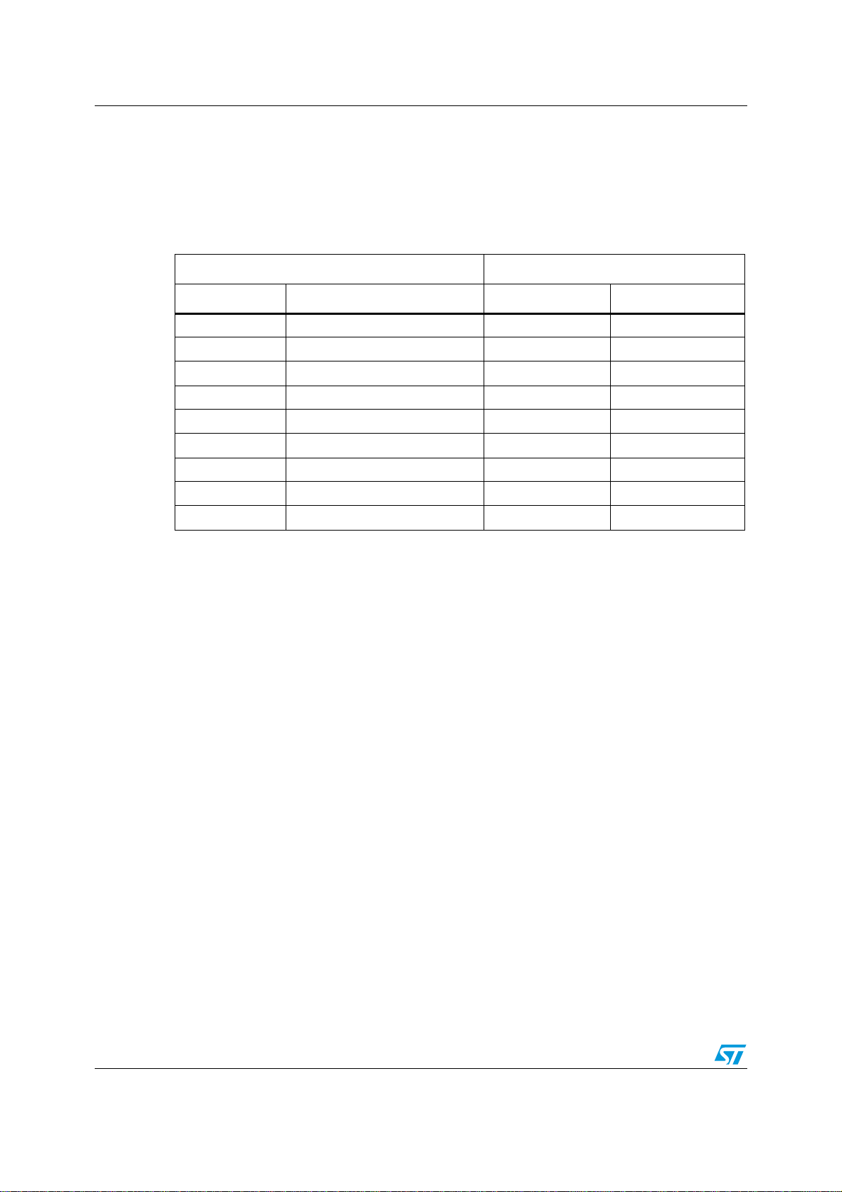
2 Microcontroller packages
The different packages available at STMicroelectronics for microcontrollers are described
Table 1.
Table 1. Microcontroller package types
Surface mount technology Through hole technology
Package Pin count Package Pin count
SON 8,16 PDIP .3 8, 16, 20
SOW 16, 20, 24, 28, 34 Shrink PDIP .4 32S
PLCC 44, 520 PDIP .6 28, 42S, 56S
PQFP 44, 52, 80, 100, 144, 208
LQFP 32, 44, 48, 52, 64, 80, 100, 128
LFBGA,TFBGA Up to 144
PBGA Up to 480
TSSOP 20
(1)
VFQFPN 8, 20, 24, 36, 40, 48, 64
1. Larger package portfolio can be proposed upon request.
Through hole technology (THT) and Surface mount technology (SMT) imply different
soldering technologies leading to different constraints.
In THT, the package body is exposed to relatively low temperatures (< 150 °C) because the
lead extremities are only dipped in the soldering alloy, whereas in SMT the whole package
body is exposed to a very high temperature (> 240 °C) during reflow soldering process.
In addition, molding compounds used for integrated circuit encapsulation absorb moisture
from the ambient medium. During rapid heating in solder reflow process (see Section 4:
Soldering for more details), this absorbed moisture can vaporize, generating pressure at
lead frame pad / silicon to plastic interfaces in the package, with a risk of package cracking
and potential degradation of device reliability.
4/15 Doc ID 14016 Rev 2
Page 5

AN2639 SMD presentation
3 SMD presentation
Unlike through hole technology where leads are inserted into the printed circuit board, SMD
(surface mount device) package is attached directly onto mounting pads of the substrate.
SMT is extensively used in electronic applications because it has the following advantages:
●
Packages are smaller and support higher pin counts
●
Packages are light and compact, thus reducing system sizes
●
Mounting can be done on either side of the PCB
●
No cost for drilling holes into the PCB
Surface mount technology also comes along with a few disadvantages:
●
Increased sensitivity to soldering heat because of their thinner dimension
●
Soldering conditions harder to determine (use of finer structures and higher pin count)
3.1 Handling SMDs
Though the intrinsic reliability of SMD packages is now excellent, the use of inappropriate
techniques or unsuitable tools during mechanical handling can affect the long term reliability
of the device, or even destroy it.
When handling a SMD package, it is strongly recommended to use adapted tools such as
vacuum pipes to avoid touching the pins as much as possible. Manual handling could affect
lead coplanarity and cause lead contamination or scratches that could generate solderability
problems. It is also not allowed to widen the interval between two consecutive pins.
Doc ID 14016 Rev 2 5/15
Page 6

Soldering AN2639
SOLDER PASTE
APPLICATION
GLUE
APPLICATION
DEVICE
MOUNTING
GLUE AGING
SOLDER PASTE
APPLICATION
SOLDERING
CLEANING
TESTING
SOLDER PASTE
APPLICATION
SOLDERING
CLEANING
TESTING
SOLDER PASTE
APPLICATION
GLUE
APPLICATION
DEVICE
MOUNTING
FLUX
APPLICATION
SOLDERING
CLEANING
TESTING
REFLOW
DOUBLE SIDED
REFLOW
SINGLE SIDED
WAVE
SOLDERING
SOLDERING
SOLDERING
VR02104B
MOUNTING
DEVICE
DEVICE
MOUNTING
4 Soldering
4.1 Soldering methods
There are 3 main soldering methods (which are detailed in Figure 1):
●
Single sided reflow soldering
●
Double sided reflow soldering
●
Wave soldering (for THT devices)
Bending leads
In all processes it is important to avoid straining the package and particularly the area where
the leads enter the encapsulating resin. If the package/lead interface is strained the
resistance to humidity and thermal stress will be compromised, affecting device reliability.
Insertion
When mounting devices on a printed circuit board the golden rule is, again, to avoid stress.
In particular, adhere to the specified pin spacing of the device: do not try to bend the leads
to fit non-standard hole spacing.
Figure 1. Soldering method descriptions
6/15 Doc ID 14016 Rev 2
Page 7

AN2639 Soldering
4.2 Soldering recommendations
The following recommendations must be followed for soldering each package type (see
Table 2).
Table 2. Package/soldering process compatibility
Reflow processing process Wave soldering process
Package
Process Reliability Process Reliability
PLCC OK OK impossible N/A
SOP OK OK feasible
QFP OK OK critical
BGA OK OK impossible N/A
VFQFPN OK OK impossible N/A
1. Reflow soldering with DIP and wave soldering with PLCC, BGA and VFQFPN are strictly impossible due to
the lead/ball configuration.
2. Wave soldering with SMT packages is not recommended because the thermal shock associated with
package body solder dipping may induced internal structural damage to the package (interface
delamination) that may affect long term reliability.
SMT Package characterizations performed as a standard by STMicroelectronics only include Solder
Reflow Resistance assessment.
JEDEC JESD22A111 recommends that wave soldering of SMT packages should be evaluated by the
USER, because the stress induced inside the package is very dependant of solder process parameters.
3. Wave soldering with PQFP is not recommended because it is difficult to avoid solder bridges when leads
pass through the double wave.
(1)
(3)
(2)
(2)
4.3 Compatibility with leaded soldering process
Lead-free packages can be assembled using leaded soldering process. For more details
about soldering process compatibilities and conditions, please refer to application note
AN2034.
Doc ID 14016 Rev 2 7/15
Page 8

Soldering AN2639
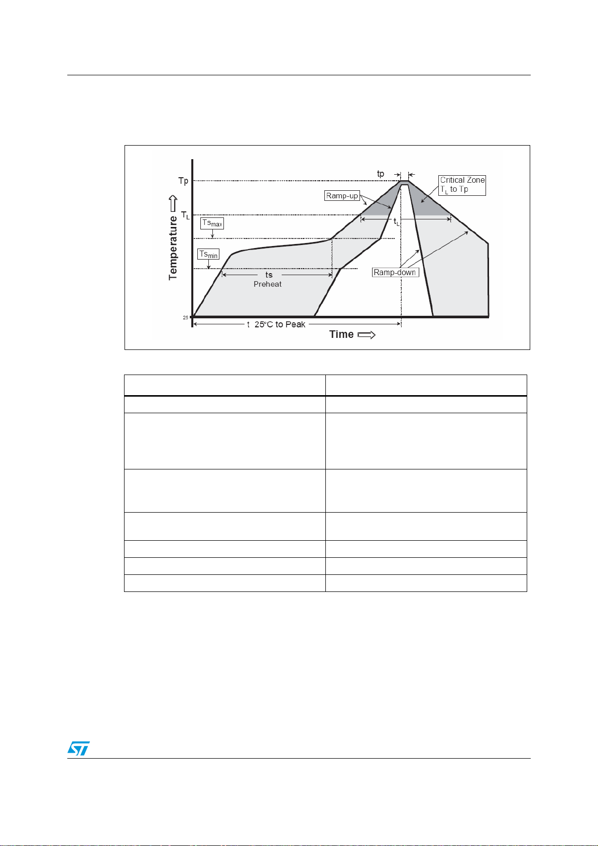
4.4 Reflow soldering conditions
The greater danger during reflow soldering is overheating. If an integrated circuit is exposed
to high temperature for an excessive period of time, it may be damaged and its reliability
reduced.
It is also important to use suitable fluxes for the soldering baths to avoid deterioration of the
leads or package resin. Residual flux between the leads or in contact with the resin must be
removed to guarantee long term reliability. The solvent used to remove excess flux should
be chosen with care. It is particular true for trichloroethylene (CHCl: CCl2). Base solvents
should be avoided because the residue could corrode the encapsulating resin.
High-quality low-defect soldering requires identifying the optimum temperature profile for
reflowing the solder paste, thus optimizing the process. The heating and cooling rise rates
must be compatible with the solder paste and components.
A typical profile consists of a preheat, dryout and reflow sections.
The most critical point in the preheat section is to minimize the temperature rise rate to less
than 2 °C/second, in order to minimize thermal shock on the semiconductor components.
The dryout section is used primarily to ensure that the solder paste is fully dried before
hitting reflow temperatures.
Solder reflow is accomplished in the reflow zone, where the solder paste is elevated to a
temperature greater than the melting solder point. Melting temperature must be exceeded
by approximately 20 °C to ensure quality reflow.
Figure 2. Typical reflow soldering profile
8/15 Doc ID 14016 Rev 2
Page 9
AN2639 Soldering
Refer to Figure 3 for the recommended reflow soldering profiles.
STMicroelectronics Lead-free packages are warranted for such reflow profile conditions.
Figure 3. Recommended reflow soldering profile
Table 3. JEDEC standard Lead-free reflow profile (according to J-STD-020D)
Profile feature Lead-free assembly
Average ramp-up rate (T
to TP) 3 °C/second max.
smax
Preheat
-Temperature Min (T
-Temparature Max (T
-Time (tL)
smin
smax
)
)
150 °C
200 °C
60-120 seconds
Time maintained above:
-Temperature (TL)
-Time (tL)
Peak/classification temperature (TP)
217°C
60-150 seconds
Package dependant, see temperature indicated
on box label.
Time within 5 °C of actual peak temperature (TP) 30 seconds
Ramp-down rate 6°C/second max.
Time 25 °C to peak temperature 8 minutes max.
1. All temperatures refer to topside of the package, measured on the body surface.
(1)
Doc ID 14016 Rev 2 9/15
Page 10

SMD gluability AN2639
VR02104F
0.25
0.5 0.75
1
OK
PROBLEM
GLUABILITY (kg / mm2)
5 SMD gluability
It is strongly recommended to follow glue application specifications from their glue supplier,
and to use 100% glue polymerization for optimal glue efficiency.
Figure 4. Recommended profiles for glue polymerization using regular oven and
linear flow oven
Figure 5. Gluability evaluation with a shear test
Various tests have shown that glue shear test specification limit conforms to the IPC SM817
standard (0.75 kg/mm2 minimum). Customer complaints usually happen when values are
below 0.5 kg/mm2. It has been verified that below 0.25 kg/mm2 components fall from PCB
during handling. General capability in plastic SMD is greater than 1 kg/mm2.
10/15 Doc ID 14016 Rev 2
Page 11

AN2639 Dry packing
6 Dry packing
Quality and reliability of SMDs after soldering depends heavily on moisture absorption
during storage. A specific packing, called dry pack, was implemented for defined conditions
at the delivery. Time and environment will modify the amount of absorbed humidity. Moisture
sensitive SMDs (SOP, PLCC, PQFP, BGA, VFQFPN) are dry packed to protect them from
moisture absorption during shipment / storage and then to reduce failure risks mainly due to
popcorn effect.
6.1 Pop-corn effect
Pop-corn effect is the cracking of the package during the soldering cycle. It has got a
growing importance due to the trends towards larger die size in integrated circuits. This
phenomenon is mainly caused by the moisture absorbed by the epoxy molding. When the
package is exposed to high temperatures, as in most SMT soldering processes, the water at
the interface between plastic and die pad vaporizes suddenly, generating high internal
pressure. Cracks may occur in the molding compound depending on the absorbed moisture
level, soldering temperature and time, die size, package structure and molding compound
characteristics.
SMD products are contained in tubes, on trays or on tape, and are then vacuum sealed in an
hermetic bag.
Opening the package will stop the ideal conditions and start the influence of the normal
environment. Figure 6 shows the recommended handling flow.
Doc ID 14016 Rev 2 11/15
Page 12

Dry packing AN2639
VR02104H
DRY PACK
DESSICANT
HUMIDITY
MARKING
DRY BAKE
TESTING
SEALING
CONTROL
INDICATOR
VACUUM
STORAGE
SOLDERING
Storage period
DELIVERED
GEL TURNED
PACK OPEN
> X Hours
(1)
?
PRODUCT
TO PINK ?
BAKE
125°C / 24 h
YES
NO
NO
YES
STMICROELECTRONICS
CUSTOMER
<25°C / <65% RH
Figure 6. Recommended flow to control package moisture absorption
6.2 Dry pack opening
12/15 Doc ID 14016 Rev 2
1. X depends on the MSL level (see JEDEC standard J-STD-020D).
Parts in dry pack are recommended to be stored in dry boxes (i.e. cabinets under nitrogen
atmosphere). See Table 4 for the recommended environmental conditions for storage when
no dry boxes are available.
Table 4. Environmental conditions
Condition Recommended value
Temperature 5 -> 30°C
Humidity 60°C max
Dust should also be minimized. There should be no vibration or shock which could distort
the packing container. To avoid excess weight packing, containers should not be stacked on
top of each other.
After opening a dry pack, soldering should be done within 24 hours. SMD products stored
over the specified storage period need to be baked at 125 °C for 24 hours (under nitrogen
atmosphere). Devices packed in tubes or in tapes must be transferred to metal tubes before
baking whereas trays are bake able.
Page 13

AN2639 Dry packing
Figure 7. Moisture absorption / drying curve
Doc ID 14016 Rev 2 13/15
Page 14

Revision history AN2639
7 Revision history
Table 5. Document revision history
Date Revision Changes
16-Oct-2007 1 Initial release
Modified tL and tP in Table 3: JEDEC standard Lead-free reflow
26-May-2009 2
profile (according to J-STD-020D).
Updated Figure 6: Recommended flow to control package
moisture absorption.
14/15 Doc ID 14016 Rev 2
Page 15

AN2639 Revision history
Please Read Carefully:
Information in this document is provided solely in connection with ST products. STMicroelectronics NV and its subsidiaries (“ST”) reserve the
right to make changes, corrections, modifications or improvements, to this document, and the products and services described herein at any
time, without notice.
All ST products are sold pursuant to ST’s terms and conditions of sale.
Purchasers are solely responsible for the choice, selection and use of the ST products and services described herein, and ST assumes no
liability whatsoever relating to the choice, selection or use of the ST products and services described herein.
No license, express or implied, by estoppel or otherwise, to any intellectual property rights is granted under this document. If any part of this
document refers to any third party products or services it shall not be deemed a license grant by ST for the use of such third party products
or services, or any intellectual property contained therein or considered as a warranty covering the use in any manner whatsoever of such
third party products or services or any intellectual property contained therein.
UNLESS OTHERWISE SET FORTH IN ST’S TERMS AND CONDITIONS OF SALE ST DISCLAIMS ANY EXPRESS OR IMPLIED
WARRANTY WITH RESPECT TO THE USE AND/OR SALE OF ST PRODUCTS INCLUDING WITHOUT LIMITATION IMPLIED
WARRANTIES OF MERCHANTABILITY, FITNESS FOR A PARTICULAR PURPOSE (AND THEIR EQUIVALENTS UNDER THE LAWS
OF ANY JURISDICTION), OR INFRINGEMENT OF ANY PATENT, COPYRIGHT OR OTHER INTELLECTUAL PROPERTY RIGHT.
UNLESS EXPRESSLY APPROVED IN WRITING BY AN AUTHORIZED ST REPRESENTATIVE, ST PRODUCTS ARE NOT
RECOMMENDED, AUTHORIZED OR WARRANTED FOR USE IN MILITARY, AIR CRAFT, SPACE, LIFE SAVING, OR LIFE SUSTAINING
APPLICATIONS, NOR IN PRODUCTS OR SYSTEMS WHERE FAILURE OR MALFUNCTION MAY RESULT IN PERSONAL INJURY,
DEATH, OR SEVERE PROPERTY OR ENVIRONMENTAL DAMAGE. ST PRODUCTS WHICH ARE NOT SPECIFIED AS "AUTOMOTIVE
GRADE" MAY ONLY BE USED IN AUTOMOTIVE APPLICATIONS AT USER’S OWN RISK.
Resale of ST products with provisions different from the statements and/or technical features set forth in this document shall immediately void
any warranty granted by ST for the ST product or service described herein and shall not create or extend in any manner whatsoever, any
liability of ST.
ST and the ST logo are trademarks or registered trademarks of ST in various countries.
Information in this document supersedes and replaces all information previously supplied.
The ST logo is a registered trademark of STMicroelectronics. All other names are the property of their respective owners.
© 2009 STMicroelectronics - All rights reserved
STMicroelectronics group of companies
Australia - Belgium - Brazil - Canada - China - Czech Republic - Finland - France - Germany - Hong Kong - India - Israel - Italy - Japan -
Malaysia - Malta - Morocco - Philippines - Singapore - Spain - Sweden - Switzerland - United Kingdom - United States of America
www.st.com
Doc ID 14016 Rev 2 15/15
 Loading...