

Page 1
AN2627
Application note
ST8R00 syncronous boost
converter with output current cut-off function
Introduction
The ST8R00 family of synchronous step-up DC-DC converters with current output cut-off
function provide up to 1 A over an input voltage range of 4 V to 6 V and an output voltage
range of 6 V to 12 V.
The high switching frequency (1.2 MHz) allows the use of tiny surface-mount components.
Along with the resistor divider to set the output voltage value, an inductor and two capacitors
are required. A low output ripple is guaranteed by the current mode PWM topology and by
the use of low ESR surface-mounted ceramic capacitors.
The device is available in two versions: burst mode (ST8R00) and continuous mode
(ST8R00W).
The ST8R00 devices are thermal protected and available in the DFN8 4x4 package.
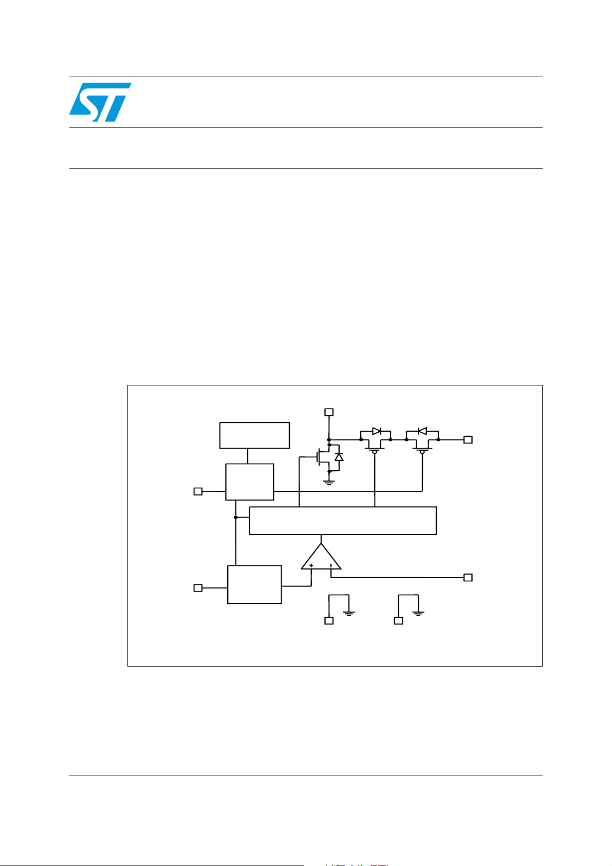
Figure 1. Simplified schematic diagram
INH
IN
Thermal
Inhibit
Vref
LX
Ns
PGND
PWM control
PGND
Ps
GND
OUT
Po
FB
AM00001v1
December 2009 Doc ID 13913 Rev 2 1/19
www.st.com
Page 2

Contents AN2627
Contents
1 ST8R00 description . . . . . . . . . . . . . . . . . . . . . . . . . . . . . . . . . . . . . . . . . . 4
1.1 Inhibit function . . . . . . . . . . . . . . . . . . . . . . . . . . . . . . . . . . . . . . . . . . . . . . 7
2 Selecting components for applications . . . . . . . . . . . . . . . . . . . . . . . . . 9
2.1 Output voltage selection . . . . . . . . . . . . . . . . . . . . . . . . . . . . . . . . . . . . . . . 9
2.2 Input capacitor . . . . . . . . . . . . . . . . . . . . . . . . . . . . . . . . . . . . . . . . . . . . . 10
2.3 Inductor . . . . . . . . . . . . . . . . . . . . . . . . . . . . . . . . . . . . . . . . . . . . . . . . . . 10
2.4 Output capacitor . . . . . . . . . . . . . . . . . . . . . . . . . . . . . . . . . . . . . . . . . . . . 10
2.5 Layout considerations . . . . . . . . . . . . . . . . . . . . . . . . . . . . . . . . . . . . . . . . 11
3 Thermal considerations . . . . . . . . . . . . . . . . . . . . . . . . . . . . . . . . . . . . . 12
4 Demonstration board usage recommendation . . . . . . . . . . . . . . . . . . . 13
4.1 External component selection . . . . . . . . . . . . . . . . . . . . . . . . . . . . . . . . . 14
4.1.1 Capacitor selection . . . . . . . . . . . . . . . . . . . . . . . . . . . . . . . . . . . . . . . . 14
4.1.2 Inductor selection . . . . . . . . . . . . . . . . . . . . . . . . . . . . . . . . . . . . . . . . . . 14
5 BOM with most-used components . . . . . . . . . . . . . . . . . . . . . . . . . . . . 16
6 Footprint recommended data . . . . . . . . . . . . . . . . . . . . . . . . . . . . . . . . . 17
7 Revision history . . . . . . . . . . . . . . . . . . . . . . . . . . . . . . . . . . . . . . . . . . . 18
2/19 Doc ID 13913 Rev 2
Page 3

AN2627 List of figures
List of figures
Figure 1. Simplified schematic diagram . . . . . . . . . . . . . . . . . . . . . . . . . . . . . . . . . . . . . . . . . . . . . . . . 1
Figure 2. ST8R00 inductor current at light load . . . . . . . . . . . . . . . . . . . . . . . . . . . . . . . . . . . . . . . . . . 4
Figure 3. ST8R00W inductor current at light load . . . . . . . . . . . . . . . . . . . . . . . . . . . . . . . . . . . . . . . . 5
Figure 4. ST8R00W inductor current at no load . . . . . . . . . . . . . . . . . . . . . . . . . . . . . . . . . . . . . . . . . 5
Figure 5. ST8R00 cut-off block . . . . . . . . . . . . . . . . . . . . . . . . . . . . . . . . . . . . . . . . . . . . . . . . . . . . . . 6
Figure 6. Current cut-off function . . . . . . . . . . . . . . . . . . . . . . . . . . . . . . . . . . . . . . . . . . . . . . . . . . . . . 6
Figure 7. Inrush current . . . . . . . . . . . . . . . . . . . . . . . . . . . . . . . . . . . . . . . . . . . . . . . . . . . . . . . . . . . . 7
Figure 8. ST8R00 application schematic . . . . . . . . . . . . . . . . . . . . . . . . . . . . . . . . . . . . . . . . . . . . . . . 7
Figure 9. Inhibit voltage vs. temperature . . . . . . . . . . . . . . . . . . . . . . . . . . . . . . . . . . . . . . . . . . . . . . . 8
Figure 10. Typical application schematic . . . . . . . . . . . . . . . . . . . . . . . . . . . . . . . . . . . . . . . . . . . . . . . . 9
Figure 11. Voltage feedback vs. temperature . . . . . . . . . . . . . . . . . . . . . . . . . . . . . . . . . . . . . . . . . . . . 9
Figure 12. Layout considerations . . . . . . . . . . . . . . . . . . . . . . . . . . . . . . . . . . . . . . . . . . . . . . . . . . . . . 11
Figure 13. The ST8R00 demonstration board . . . . . . . . . . . . . . . . . . . . . . . . . . . . . . . . . . . . . . . . . . . 13
Figure 14. Demonstration board layers . . . . . . . . . . . . . . . . . . . . . . . . . . . . . . . . . . . . . . . . . . . . . . . . 13
Figure 15. Demonstration board schematic . . . . . . . . . . . . . . . . . . . . . . . . . . . . . . . . . . . . . . . . . . . . . 14
Figure 16. Efficiency vs. output current . . . . . . . . . . . . . . . . . . . . . . . . . . . . . . . . . . . . . . . . . . . . . . . . 15
Figure 17. Efficiency vs. output voltage . . . . . . . . . . . . . . . . . . . . . . . . . . . . . . . . . . . . . . . . . . . . . . . . 15
Figure 18. ST8R00 efficiency vs. inductor . . . . . . . . . . . . . . . . . . . . . . . . . . . . . . . . . . . . . . . . . . . . . . 15
Figure 19. ST8R00W efficiency vs. inductor . . . . . . . . . . . . . . . . . . . . . . . . . . . . . . . . . . . . . . . . . . . . 16
Figure 20. DFN8 4x4 recommended footprint . . . . . . . . . . . . . . . . . . . . . . . . . . . . . . . . . . . . . . . . . . . 17
Doc ID 13913 Rev 2 3/19
Page 4
ST8R00 description AN2627
1 ST8R00 description
The ST8R00 is a family of adjustable current mode PWM synchronous step-up DC-DC
converters with internal 1 A power switch. It represents a complete 1 A switching regulator
with internal compensation which eliminates the need for additional components.
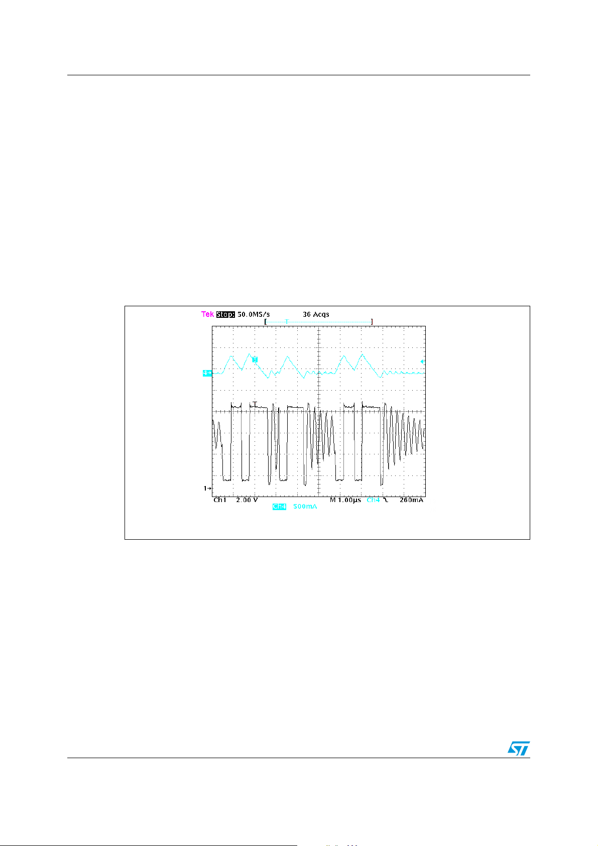
The two devices in the family, the ST8R00 and ST8R00W, operate at light load in two
different ways. The ST8R00 works in power-save mode to achieve good efficiency, as
shown in Figure 2. The ST8R00W, in order to guarantee the lowest switching ripple,
operates in PWM (pulse width modulation) mode as show in Figure 3 and Figure 4.
At medium and high load current, both versions operate in PWM mode.
The thermal shutdown block turns off the regulator when the junction temperature exceeds
150 °C (typ), and the cycle-by-cycle current limiting provides protection against overcurrent
sink.
Figure 2. ST8R00 inductor current at light load
VIN=5 V, V
OUT
=8 V, I
=60 mA, Ch1=LX, Ch4=I
OUT
I
L
LX
L
4/19 Doc ID 13913 Rev 2
Page 5
AN2627 ST8R00 description
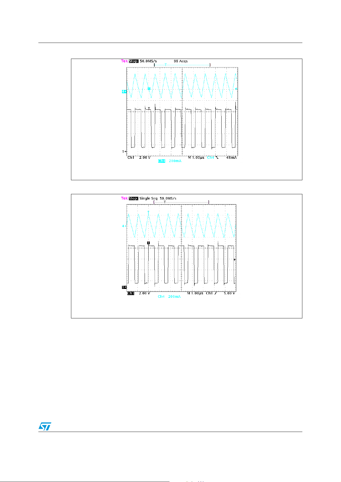
Figure 3. ST8R00W inductor current at light load
I
L
LX
VIN=5 V, V
OUT
=8 V, I
=60 mA, Ch1=LX, Ch4=I
OUT
L
Figure 4. ST8R00W inductor current at no load
I
L
LX
VIN=5 V, V
=8 V, no load Ch1=LX, Ch4=I
OUT
L
For proper functioning of the device, only a few components are required: an inductor, two
capacitors and the resistor divider. The inductor chosen must not saturate at the operating
peak current. Its value should be selected taking into account that a large inductor value
reduces output voltage ripple, while a smaller inductor can be selected when it is important
to reduce package size and the total cost of the application. Finally, the ST8R00 family has
been designed to work properly with X5R or X7R SMD ceramic capacitors both at the input
and at the output. These types of capacitors, thanks to their very low series resistance
(ESR), minimize the output voltage ripple. Other low ESR capacitors can be used in
accordance with application requirements without compromising the correct functionality of
the device.
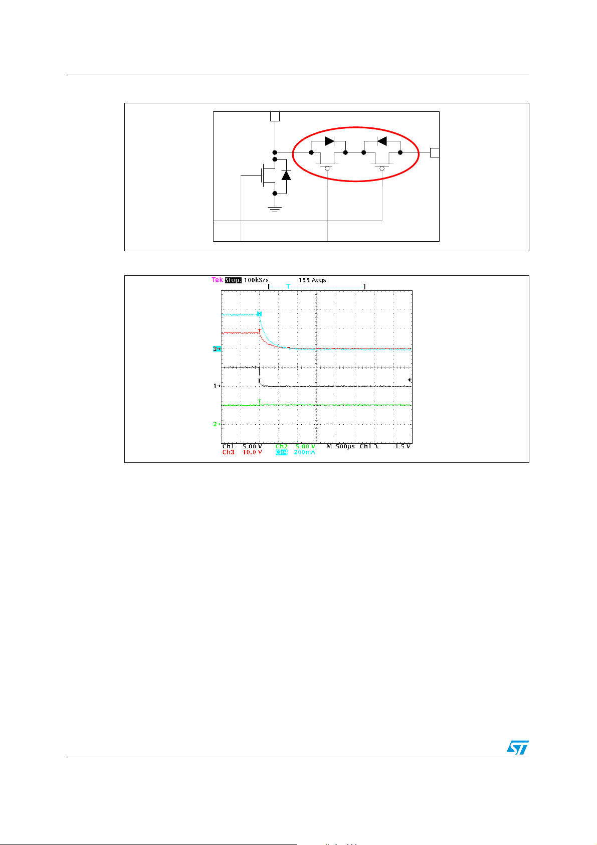
This device features an output current cut-off function. Two P-channel MOSFETs in a backto-back configuration, as shown in Figure 5, stop the output current when the inhibit is low
(Figure 6).
Doc ID 13913 Rev 2 5/19
Page 6
ST8R00 description AN2627
Figure 5. ST8R00 cut-off block
LX
LX
OUT
OUT
Ns
Ns
PGND
PGND
Figure 6. Current cut-off function
Ps
Ps
Po
Po
Iout
Vout
Inh
Vin
Figure 7 shows the in-rush current at start-up. Initially, the C
discharged and the current limitation is due only to the equivalent series resistor of the
inductor, the power MOSFET parasitic diode and the cut-off MOSFETs’ R
the output voltage reaches the input voltage level, the device begins to switch and the
current is limited cycle by cycle.
6/19 Doc ID 13913 Rev 2
capacitor is completely
OUT
DS(ON)
. As soon as
Page 7

AN2627 ST8R00 description
Figure 7. Inrush current
=4.5 V, V
V
IN
OUT
=7 V, V
INH
1.1 Inhibit function
The ST8R00 family of devices also include an inhibit function (pin 6). When the INH voltage
is higher than 2 V, the device is ON and if it is lower than 0.8 V, the device is OFF.
The INH pin does not have an internal pull-up, which means that the pin cannot be left
floating.
from 0 V to 3 V, R
=13 Ω, L=10 µH, CIN=C
LOAD
Vout
Iin
LX
OUT
=10 µF
If the inhibit function is not used, the INH pin must be connected to V
in Figure 8 below.
Figure 8. ST8R00 application schematic
L
L
Vin
Vin
41
41
IN LX
Cin
Cin
Rinh
Rinh
Cinh
Cinh
IN LX
6
6
INH
INH
ST8R00
7
7
HV
HV
GND PGND
GND PGND
ST8R00
23
23
OUT
OUT
FB
FB
8
8
5
5
as in the schematic
IN
Vout
Vout
R1
R1
Cout
Cout
R2
R2
Doc ID 13913 Rev 2 7/19
Page 8

ST8R00 description AN2627
Figure 9. Inhibit voltage vs. temperature
2
1.8
1.6
1.4
1.2
1
0.8
Vinh [V]
0.6
0.4
0.2
Vin=4V, Vinh from 0 to 2V, Iout=50mA,
L=4.7µH, Cin=10µF, Cout=10µF
ON OFF
0
-75 -50 -25 0 25 50 75 100 125 150 175
T [°C]
8/19 Doc ID 13913 Rev 2
Page 9

AN2627 Selecting components for applications
2 Selecting components for applications
This section provides information to assist in the selection of the most appropriate
components for applications.
Figure 10 shows a typical application schematic diagram.
Figure 10. Typical application schematic
L
L
Vin
Vin
41
Cin
Cin
OFF ON
OFF ON
41
8
OUT
OUT
FB
FB
8
5
5
IN LX
IN LX
6
6
INH
INH
ST8R00
7
7
HV
HV
ST8R00
GND PGND
GND PGND
23
23
R1
R1
R2
R2
Vout
Vout
Cout
Cout
2.1 Output voltage selection
The output voltage can be adjusted from 6 V up to 12 V by connecting a resistor divider
between the output and the FB pin.
The resistor divider should be chosen in accordance with the following equation:
Equation 1
V
outVFB
The feedback voltage versus temperature is shown Figure 11 below.
It is recommended to use a resistor with a value in the range of 10 kΩ to 100 kΩ. Lower
values can be suitable as well, but will increase current consumption.
Figure 11. Voltage feedback vs. temperature
1.3
1.28
1.26
1.24
1.22
1.2
1.18
Vfb [mV]
1.16
1.14
1.12
1.1
-75 -50 -25 0 25 50 75 100 125 150 175
Vin=Vinh=5V, Iout=50mA,
L=4.7µH, Cin=10µF, Cout=10µF
R
1
1
------ -+=
with
V
1.22 V=
R
2
FB
T [°C]
Doc ID 13913 Rev 2 9/19
Page 10

Selecting components for applications AN2627
2.2 Input capacitor
The input capacitor must be able to provide AC ripple current to the inductor and to
withstand the maximum input operating voltage.
Another important function of the input capacitor is to limit noise and therefore the
interference with the other blocks connected to the same network.
The quality of these capacitors must to be quite high to minimize the power dissipation
generated by the internal ESR, thereby improving system reliability and efficiency.
Various capacitors can be considered:
● Ceramic capacitors - These capacitors usually have a higher RMS current rating for a
given physical dimension (due to the very low ESR). The drawback is the high cost of
capacitors with very large values.
● Electrolytic capacitor - The availability of small size tantalum capacitors with very low
ESR is increasing. However, they are subject to thermal damage if subjected to very
high current during charge. Since they can, in fact, be subjected to high surge current
when connected to the power supply, it is better to avoid using this type of capacitor for
the input filter of the device. Aluminum capacitors are not the best choice due to their
high ESR.
2.3 Inductor
The inductor value is very important because it establishes the ripple current. The
approximate inductor value is obtained with the following formula:
Equation 2
where T
usually fixed at 20-40% of I
is the ON time of the internal switch, given by D · TSW. The ripple current, ΔIL, is
ON
IN_MAX.
Equation 3
where η is the efficiency.
2.4 Output capacitor
The output capacitor is very important to satisfy the output voltage ripple requirement. To
reduce the output voltage ripple, a low ESR capacitor is required.
The output voltage ripple (V
RIPPLE
Vin
=
Δ
OUT_max
T
ON
I
L
⋅
VoutI
η⋅
Vin
I
IN_MAX
L ⋅
=
), in continuous mode is:
Equation 4
⎛⎞
V
RIPPLEIout
where F
10/19 Doc ID 13913 Rev 2
is the switching frequency.
SW
⋅=
ESR
⎝⎠
V
–()
outVin
------------------------------------------- -+
V
⋅⋅
outCoutFSW
Page 11

AN2627 Selecting components for applications
2.5 Layout considerations
Due to the high switching frequency and peak current, the layout is an important design step
for all switching power supplies. If the layout is not done carefully, important parameters
such as efficiency and output voltage ripple could be out of specification.
Short, wide traces must be implemented for main current and for power ground paths as
shown in bold in
IC pins as well as the inductor and output capacitor.
Figure 12. The input capacitor must be placed as close as possible to the
A common ground node minimizes ground noise, as shown in
The HV pin must be floating or connected to GND and the exposed pad of the package must
be connected to the common ground node.
Figure 12. Layout considerations
L
L
Vin
Vin
41
41
IN LX
IN LX
OUT
OUT
FB
FB
2
2
Cin
Cin
OFF ON
OFF ON
6
6
INH
INH
ST8R00
GND
GND
ST8R00
PGND
PGND
3
3
7
7
HV
HV
Figure 12.
8
8
5
5
R1
R1
R2
R2
Cout
Cout
Vout
Vout
Doc ID 13913 Rev 2 11/19
Page 12

Thermal considerations AN2627
3 Thermal considerations
The dissipated power of the device is related to three different sources:
● Switching losses due to the (not negligible) R
Equation 5
DSON_NON_N
OUT
and
Equation 6
. These are equal to:
DS(ON)
D)]²D1/(I[RP
⋅−⋅=
2
OUTDSON_PEQON_P
D)1(IRP
−⋅⋅=
where D is the duty cycle of the application and R
DS(ON)_PEQ=RDS(ON)_PS+RDS(ON)_PO
.
Note: the duty cycle is theoretically given by:
V
in
1
-------------–
V
out
but in practice it is quite higher than this value to compensate for the losses of the overall
application. For this reason, the switching losses related to the R
increase compared
DS(ON)
to an ideal case.
● Switching losses due to its turning on and off. These are calculated using the following
equation:
Equation 7
)t(t
+
OFFON
2
where tON and t
IVP ⋅⋅⋅=⋅
⋅⋅=
OUTINSW
are the overlap times of the voltage across the power switch and the
OFF
current flowing into it during the turn-on and turn-off phases. t
is the equivalent switching
R-F
FtIVF
SWF-ROUTINSW
time.
● Quiescent current losses:
Equation 8
IVP ⋅=
QINQ
where IQ is the quiescent current.
The overall losses are:
Equation 9
DSON_NTOT
OUT
The junction temperature of device will be:
Equation 10
where TA is the ambient temperature and R
thJA
ambient.
12/19 Doc ID 13913 Rev 2
2
OUTDSON_PEQ
PRTT ⋅+=
TOTthJAAJ
is the thermal resistance junction-to-
IVFtIVD)1(IRD)²D1/I(RP ⋅+⋅⋅⋅+−⋅⋅+⋅−⋅=
QINSWF-ROUTIN
Page 13

AN2627 Demonstration board usage recommendation
4 Demonstration board usage recommendation
The demonstration board shown in Figure 13 is provided with a Kelvin connection, so for
each pin there are two lines available: one used to supply or sink current, and the other used
to perform the needed measurement.
The ST8R00 inhibit pin does not have an internal pull-up, so the inhibit pin cannot be left
floating.
Figure 13. The ST8R00 demonstration board
Figure 14. Demonstration board layers
Top layer
The board has one inhibit pin available, located on the top left of the board.
The inhibit pin can be used to supply an external voltage higher than 2 V to turn on the
device, or an external voltage lower than 0.8 V to turn off the device.
Bottom layer
Doc ID 13913 Rev 2 13/19
Page 14

Demonstration board usage recommendation AN2627
4.1 External component selection
Figure 15 shows the schematic diagram of the demonstration board.
Figure 15. Demonstration board schematic
L
L
Vin
Vin
41
41
8
OUT
OUT
FB
FB
8
R1
R1
5
5
R2
R2
Cin
Cin
OFF ON
OFF ON
IN LX
IN LX
6
6
INH
INH
ST8R00
7
7
HV
HV
ST8R00
GND PGND
GND PGND
23
23
In order to obtain the needed output voltage, the resistor divider must be selected based on
the following formula:
Vout
Vout
Cout
Cout
Equation 11
Table 1. Recommended resistor divider
V
out
8 V 56 kΩ 10 kΩ
9.5 V 68 kΩ 10 kΩ
The resistors in Ta bl e 1 represent a good compromise in terms of current consumption and
minimum output voltage.
4.1.1 Capacitor selection
It is possible to use any X5R or X7R ceramic capacitor:
● C
● C
=10 µF (ceramic) or higher
IN
=10 µF (ceramic) or higher. It is possible to put several capacitors in parallel to
OUT
reduce the equivalent series resistance and improve the ripple present in the output
voltage.
4.1.2 Inductor selection
V
outVFB
R1
1
------- -+=
with
R2
R1 R2
VFB1.22 V=
Due to the high (1.2 MHz) frequency, it is possible to use very small inductor values. In the
demonstration board, the device was tested with inductors in the range of 1 µH to 10 µH,
with very good efficiency performance (see
Figure 18 and Figure 19).
Because the device is able to provide an operating output current of 1 A, we strongly
recommend the use of inductors capable of managing at least 3.5 A.
14/19 Doc ID 13913 Rev 2
Page 15

AN2627 Demonstration board usage recommendation
Figure 16. Efficiency vs. output current
100
90
80
70
60
50
Efficiency [%]
40
30
Vin=5V , Vinh=5V, L=4.7µH,
Cin=10µF, Cout=10µF, Vout=8V
ST8R00
ST8R00W
20
0 0.1 0.2 0.3 0.4 0.5 0.6 0.7 0.8 0.9 1
Iout [A]
Figure 17. Efficiency vs. output voltage
100
95
90
85
80
75
70
Efficiency [%]
65
60
55
50
4.5 5.5 6.5 7.5 8.5 9.5 10.5 11.5 12.5
Vin=5V , Vinh=5V, L=4.7µH, Cin=10µF,
Cout=10µF, Iout=300mA
ST8R00
ST8R00W
Vout [V]
Figure 18. ST8R00 efficiency vs. inductor
100
90
80
70
60
50
Efficiency [%]
40
Vin=5V , Vinh=5V, Vout=8V,
Cin=10µF, Cout=10µF
30
20
0246810
Doc ID 13913 Rev 2 15/19
Iout=300mA
Iou t=0 .5A
Iou t=1 A
L [µH]
Page 16

BOM with most-used components AN2627
Figure 19. ST8R00W efficiency vs. inductor
100
90
80
70
60
50
Efficiency [%]
40
Vin=5V , Vinh=5V, Vout=8V,
Cin=10µF, Cout=10µF
30
Iou t=3 0 0mA
Iou t=0 .5A
Iou t=1 A
20
0246810
L [µH]
5 BOM with most-used components
Table 2. Bill of materials
Name Value Material Manufacturer Part numbers
C
IN
C
OUT
L 4.7 µH Coiltronics DR73-4R7
10 µF Ceramic Murata GRM31CR61E106KA12B
10 µF Ceramic Murata GRM31CR61E106KA12B
16/19 Doc ID 13913 Rev 2
Page 17

AN2627 Footprint recommended data
6 Footprint recommended data
Figure 20. DFN8 4x4 recommended footprint
Doc ID 13913 Rev 2 17/19
Page 18

Revision history AN2627
7 Revision history
Table 3. Document revision history
Date Revision Changes
13-May-2008 1 Initial release
03-Dec-2009 2 Modified Equation 9: on page 12.
18/19 Doc ID 13913 Rev 2
Page 19

AN2627
Please Read Carefully:
Information in this document is provided solely in connection with ST products. STMicroelectronics NV and its subsidiaries (“ST”) reserve the
right to make changes, corrections, modifications or improvements, to this document, and the products and services described herein at any
time, without notice.
All ST products are sold pursuant to ST’s terms and conditions of sale.
Purchasers are solely responsible for the choice, selection and use of the ST products and services described herein, and ST assumes no
liability whatsoever relating to the choice, selection or use of the ST products and services described herein.
No license, express or implied, by estoppel or otherwise, to any intellectual property rights is granted under this document. If any part of this
document refers to any third party products or services it shall not be deemed a license grant by ST for the use of such third party products
or services, or any intellectual property contained therein or considered as a warranty covering the use in any manner whatsoever of such
third party products or services or any intellectual property contained therein.
UNLESS OTHERWISE SET FORTH IN ST’S TERMS AND CONDITIONS OF SALE ST DISCLAIMS ANY EXPRESS OR IMPLIED
WARRANTY WITH RESPECT TO THE USE AND/OR SALE OF ST PRODUCTS INCLUDING WITHOUT LIMITATION IMPLIED
WARRANTIES OF MERCHANTABILITY, FITNESS FOR A PARTICULAR PURPOSE (AND THEIR EQUIVALENTS UNDER THE LAWS
OF ANY JURISDICTION), OR INFRINGEMENT OF ANY PATENT, COPYRIGHT OR OTHER INTELLECTUAL PROPERTY RIGHT.
UNLESS EXPRESSLY APPROVED IN WRITING BY AN AUTHORIZED ST REPRESENTATIVE, ST PRODUCTS ARE NOT
RECOMMENDED, AUTHORIZED OR WARRANTED FOR USE IN MILITARY, AIR CRAFT, SPACE, LIFE SAVING, OR LIFE SUSTAINING
APPLICATIONS, NOR IN PRODUCTS OR SYSTEMS WHERE FAILURE OR MALFUNCTION MAY RESULT IN PERSONAL INJURY,
DEATH, OR SEVERE PROPERTY OR ENVIRONMENTAL DAMAGE. ST PRODUCTS WHICH ARE NOT SPECIFIED AS "AUTOMOTIVE
GRADE" MAY ONLY BE USED IN AUTOMOTIVE APPLICATIONS AT USER’S OWN RISK.
Resale of ST products with provisions different from the statements and/or technical features set forth in this document shall immediately void
any warranty granted by ST for the ST product or service described herein and shall not create or extend in any manner whatsoever, any
liability of ST.
ST and the ST logo are trademarks or registered trademarks of ST in various countries.
Information in this document supersedes and replaces all information previously supplied.
The ST logo is a registered trademark of STMicroelectronics. All other names are the property of their respective owners.
© 2009 STMicroelectronics - All rights reserved
STMicroelectronics group of companies
Australia - Belgium - Brazil - Canada - China - Czech Republic - Finland - France - Germany - Hong Kong - India - Israel - Italy - Japan -
Malaysia - Malta - Morocco - Philippines - Singapore - Spain - Sweden - Switzerland - United Kingdom - United States of America
www.st.com
Doc ID 13913 Rev 2 19/19
 Loading...