

Page 1
AN2623
Application note
Evaluation board
for off-line forward converter based on L5991
Introduction
This application note gives a practical example of a 160 W, isolated, forward converter using
the L5991, high frequency current mode PWM controller. Design procedures for both the
power stage and controller are presented.
Generally for this power level the norm ICE61000-3-2 imposes the use of a PFC preregulator stage, but some countries do not require compliance to this norm. The forward
converter presented here does not have a PFC.
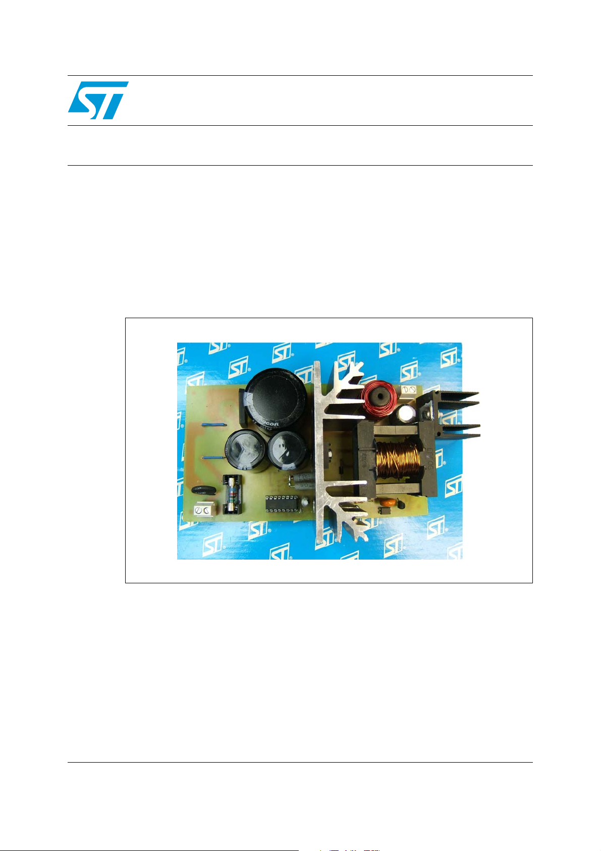
Figure 1. 160 W off-line forward converter, evaluation board
October 2007 Rev 1 1/25
www.st.com
Page 2

Contents AN2623
Contents
1 Basis of forward topology . . . . . . . . . . . . . . . . . . . . . . . . . . . . . . . . . . . . 4
2 Main characteristics . . . . . . . . . . . . . . . . . . . . . . . . . . . . . . . . . . . . . . . . . 5
3 Design circuit . . . . . . . . . . . . . . . . . . . . . . . . . . . . . . . . . . . . . . . . . . . . . . . 7
3.1 Primary controller: L5991 . . . . . . . . . . . . . . . . . . . . . . . . . . . . . . . . . . . . . . 7
3.2 Output filter . . . . . . . . . . . . . . . . . . . . . . . . . . . . . . . . . . . . . . . . . . . . . . . . . 7
3.3 Output diodes . . . . . . . . . . . . . . . . . . . . . . . . . . . . . . . . . . . . . . . . . . . . . . . 8
3.4 Power transformer design and MOSFET choice . . . . . . . . . . . . . . . . . . . . 9
3.5 Feedback loop . . . . . . . . . . . . . . . . . . . . . . . . . . . . . . . . . . . . . . . . . . . . . 13
4 Experimental results . . . . . . . . . . . . . . . . . . . . . . . . . . . . . . . . . . . . . . . . 15
4.1 High frequency ripple of output voltage and load regulation . . . . . . . . . . 16
4.2 Dynamic load test . . . . . . . . . . . . . . . . . . . . . . . . . . . . . . . . . . . . . . . . . . . 18
4.3 Start-up behavior . . . . . . . . . . . . . . . . . . . . . . . . . . . . . . . . . . . . . . . . . . . 19
4.4 Wake-up time . . . . . . . . . . . . . . . . . . . . . . . . . . . . . . . . . . . . . . . . . . . . . . 20
4.5 Short circuit test . . . . . . . . . . . . . . . . . . . . . . . . . . . . . . . . . . . . . . . . . . . . 21
4.6 Thermal measurement and global efficiency . . . . . . . . . . . . . . . . . . . . . . 22
5 Revision history . . . . . . . . . . . . . . . . . . . . . . . . . . . . . . . . . . . . . . . . . . . 24
2/25
Page 3

AN2623 List of figures
List of figures
Figure 1. 160 W off-line forward converter, evaluation board . . . . . . . . . . . . . . . . . . . . . . . . . . . . . . . 1
Figure 2. Basic forward converter topology . . . . . . . . . . . . . . . . . . . . . . . . . . . . . . . . . . . . . . . . . . . . . 4
Figure 3. Reset circuits . . . . . . . . . . . . . . . . . . . . . . . . . . . . . . . . . . . . . . . . . . . . . . . . . . . . . . . . . . . . 4
Figure 4. Electrical schematic . . . . . . . . . . . . . . . . . . . . . . . . . . . . . . . . . . . . . . . . . . . . . . . . . . . . . . . 6
Figure 5. Vds and Ids of STW12NK90Z in full load condition at different input voltages . . . . . . . . . 15
Figure 6. High frequency ripple of output voltage in full load condition at different input voltages. . . 16
Figure 7. Output voltage behavior against the load and the V
Figure 8. Behavior of system under dynamic load at different input voltages . . . . . . . . . . . . . . . . . . 18
Figure 9. Behavior of system under dynamic load at different input voltages . . . . . . . . . . . . . . . . . . 19
Figure 10. Wake-up time of the system at different input voltages . . . . . . . . . . . . . . . . . . . . . . . . . . . 20
Figure 11. Behavior of the system in short circuit condition at different input voltages . . . . . . . . . . . . 21
Figure 12. Efficiency of the system . . . . . . . . . . . . . . . . . . . . . . . . . . . . . . . . . . . . . . . . . . . . . . . . . . . 22
. . . . . . . . . . . . . . . . . . . . . . . . . . . . . 17
in
3/25
Page 4
Basis of forward topology AN2623
R
R
R
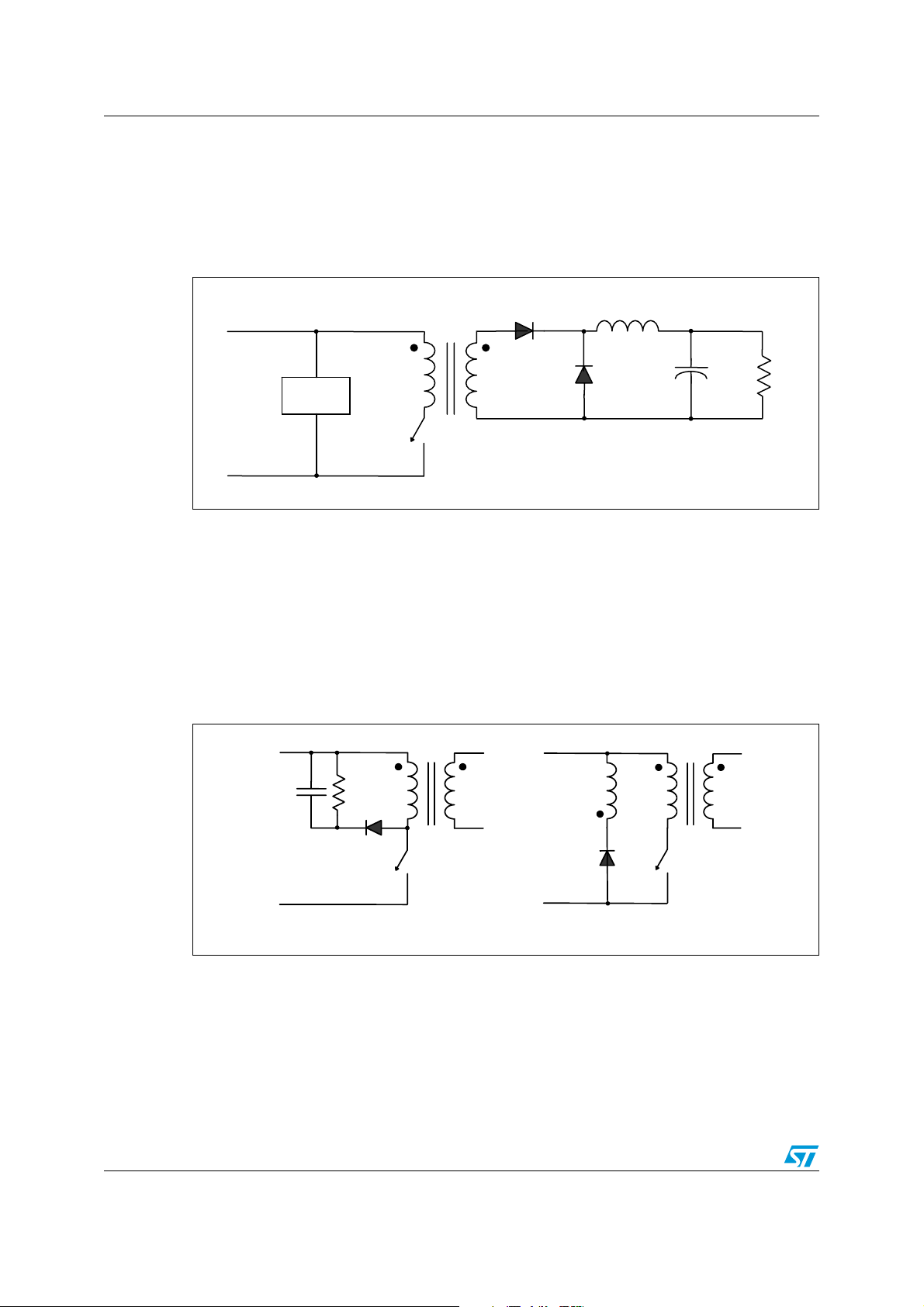
1 Basis of forward topology
A forward converter is typically used in off-line applications in the 100 W - 300 W power
range. A simplified schematic of the forward converter can be seen in Figure 2.
Figure 2. Basic forward converter topology
D
1
V
d
Reset
Circuit
L
V
D
2
C
0
_
_
A natural limitation of the forward converter is the need to completely reset the transformer,
cycle by cycle, before the next MOSFET switches on. Different circuits are used for this
purpose with advantages and drawbacks. The two simplest and most commonly used reset
schemes are: the RCD reset circuit and the reset auxiliary winding both shown in Figure 3
(a-b). In the design presented in this document, the reset winding was used. It is
advantageous with respect to efficiency because the energy stored in the magnetizing
inductor goes back to the input and is not lost as using an RCD snubber net. The drawback
of the reset circuit is that, generally, a higher voltage Power Mosfet is needed. In the present
design a 900 V MOSFET was used.
Figure 3. Reset circuits
C
R
N
1
D
(a) (b)
The primary controller IC used is the L5991. It is based on a standard current mode PWM
controller and includes features such as programmable soft start, adjustable duty cycle
limitation and a standby function that reduces the switching frequency when the converter is
lightly loaded. The standby function, in this case, is not used to prevent the transformer from
saturation. The output voltage regulation is obtained through a voltage reference and an
error amplifier (TL1431) placed at the secondary side. A charge pump connected to an
auxiliary winding guarantees a stable supply at the controller itself.
4/25
N
2
N
R
N
1
D
R
N
2
Page 5

AN2623 Main characteristics
2 Main characteristics
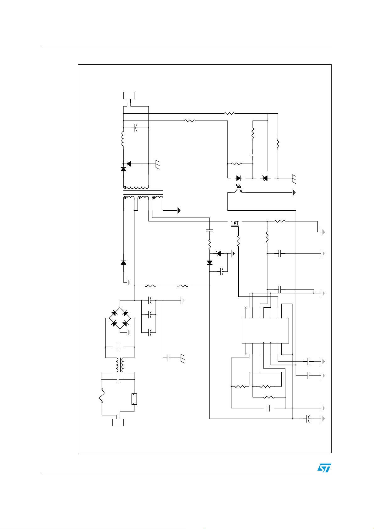
The design procedure is presented in this section and we will refer to the electrical
schematic in Figure 4. The power supply electrical specifications are shown in Tabl e 1
below.
Table 1. Input and output parameters
Input parameters
f
V
line
in
Input voltage 88 ÷ 290 V
Line frequency 50/60 Hz
Output parameters
V
out
I
out
P
out
Output voltage 35 V
Output current 4.5 A max continuous, 0.45 A min
Output power 160 W max
Efficiency at full load 80%
∆V
% Max tolerance on output voltage 3%
out
∆V
T
out HF
A max
Max output voltage ripple at switching frequency 350 mV
Maximum ambient temperature 70 °C
RMS
5/25
Page 6
Main characteristics AN2623
e
e
e
e
e
e
Figure 4. Electrical schematic
1
2
J2
CON2J2CON2
R5
15 kOhm
R5
15 kOhm
+
+
C1
L1
390 uH-5A
L1
390 uH-5A
DN1
DN1
BYT16P-400 heatsink
BYT16P-400 heatsink
16
T1
T1
5
C1
270uF, ESR=42 mOhm, 50 V
270uF, ESR=42 mOhm, 50 V
143
1
4
8
7
R3
R3
5.6 kOhm
5.6 kOhm
TRAN_ISDN_06
TRAN_ISDN_06
0
R6
R6
12
OPTO 1
OPTO 1
43
R7
R7
C8
1.2 kOhm
1.2 kOhm
ISO1
ISO1
Q1
Q1
20 kOhm
20 kOhm
6 nFC86 nF
3
TL 431
TL 431
......1
......1
2 1
R9
R9
R10
R10
1.153 kOhm (+/- 1%)
1.153 kOhm (+/- 1%)
0
<Doc> <R
<Doc> <R
<Doc> <R
<Doc> <R
<Doc> <R
<Doc> <R
A
A
A
A
A
A
Title
Size Document Number Rev
Title
Size Document Number Rev
Title
Size Document Number Rev
Title
Size Document Number Rev
Title
Size Document Number Rev
Title
Size Document Number Rev
3
LFILTERIN1
LFILTERIN1
HT3545-472Y4R0-T01
HT3545-472Y4R0-T01
FUSE14AFUSE1
4A
D1
STTH110
D1
STTH110
0
1
600V-6A
600V-6A
DIODE BRIDGE1
DIODE BRIDGE1
4
0
-+
-+
2
CB1
CB1
2 3
47 nF X2 Cap
47 nF X2 Cap
1 4
CA1
CA1
NTC1
NTC1
47 nF X2 Cap
47 nF X2 Cap
1
2
J1
CON2J1CON2
+
+
C4
C4
330 uF, 450V
330 uF, 450V
+
+
C3
C3
+
+
C2
C2
100 uF, 450V
100 uF, 450V
2.5 Ohm
2.5 Ohm
R1
220 kOhm, 1/4W
R1
220 kOhm, 1/4W
100 uF, 450V
100 uF, 450V
C5
C5
2.2 nF Y1 Cap
2.2 nF Y1 Cap
R2
R2
220 kOhm,1/4W
220 kOhm,1/4W
0
C6
R4
R4
50 Ohm-1/2W
50 Ohm-1/2W
D2
33nFC633nF
D3
1N4148D21N4148
+
+
C7
C7
15VD315V
10uF, 20V
10uF, 20V
STW12NK90Z-heatsink
STW12NK90Z-heatsink
Rg
Rg
10 OHM1
10 OHM1
0
14
16
15
DIS
ST-BY
DC-LIM
Sync1RCT2DC3Vref4Vfb5Vcomp6SS7Vcc
U1
RA1
4.7 kOhm
RA1
4.7 kOhm
13
12
ISEN
SGND
RDOWN1
RDOWN1
CT1
CT1
4.7 nF
4.7 nF
R8
R8
2.2 kOhm
2.2 kOhm
11
PGND
RUP1
RUP1
4.7 kOhm
4.7 kOhm
3.6 kOhm
3.6 kOhm
0.21 Ohm
0.21 Ohm
C10
C10
C9
9
10
Vc
Vout
8
100 pF
100 pF
100 pFC9100 pF
L5991U1L5991
C12
C12
+
+
C11
C11
C13
C13
33 nF
33 nF
1 nF
1 nF
22uF, 25V
22uF, 25V
0
0
0 0
0
0 0
6/25
Page 7

AN2623 Design circuit
3 Design circuit
This section describes the design of the major parts of the circuit.
3.1 Primary controller: L5991
As previously stated, the L5991 is used as the primary controller and its components must
first be selected. Refer to the L5991 datasheet for the choice of the two resistors (R
and one capacitor (C
oscillator in normal operation (f
established that the device must work at the unique frequency (in this case R
) which allows setting separately the operating frequency of the
T
) and in standby mode (fsb). In this application, it was
osc
B
kHz in normal and in standby operation. This frequency is calculated using R
following formula:
Equation 1
f
osc
-------------------------------------------------------------- -=
C
T
1
0.693 RAKT+⋅()⋅
, RB )
A
→ ∝ ) of 60
in the
A
where K
T
=5%T
d
=160 Ω and CT is calculated fixing the discharge oscillator capacitor time
T
sw
Equation 2
Establishing a D
max
method that allows implementing the slope compensation, if needed, was used.
The duty cycle limitation is obtained by applying the following voltage to pin3 :
Equation 3
fixing (refer to Figure 4) R
3.2 Output filter
Admitting a max current ripple on the inductor ∆I
necessary to select an inductor value according to Equation 4:
Equation 4
T
30 109–KtCtCt4.7= nF RA5.6 k Ω=,⇒⋅+⋅=
d
= 50%, L5991 allows obtaining this last value in two different ways. The
2D
–()
52
V
3
=4.70 kΩ, we can then immediately calculate R
up
V
– V
2minVdiode
L
-------------------------------------------------------
out
∆I
out
max
V32.17 V=⇒–=
=3.60 kΩ.
down
equal to 20% of I
Lout
out
D
max
------------- -
f
sw
342 µH=⇒⋅=
L
out
–
outMAX
, it is
The RMS (root mean square) current through the inductor is given by Equation 5:
Equation 5
I
RMS Lout–
2
I
out
2
∆
out
-------------+ I
12
RMS Lout–
4.58 A=⇒=
7/25
Page 8

Design circuit AN2623
The peak current through the inductor is:
Equation 6
I
Peak Lout–
I
out∆ILoutIPeak Lout–
5.4 A==+=
According to these results, L
whose inductance value is L
According to the max high frequency voltage ripple (∆
specifications, the necessary minimum capacitor value (C
was chosen as the Coil Craft's inductor PCV-1-394-05L
out
=390 µH.
out
=350 mV) from the electrical
VoutHF
in the Figure 4) and its maximum
1
admitted ESR (Equivalent Series Resistance) are calculated as follows:
Equation 7
C
outmin
V
out
--------------------- -
∆V
outHF
-------------------- -
⋅
8f
1D
sw
–
max
---------------------- -
L
out
C
outmin
4.5 µF=⇒⋅⋅=
1
2
Equation 8
∆V
outHF
max
--------------------- -
∆I
out
ESR
max
388 mΩ=⇒=
ESR
The RMS current through the output capacitor must not exceed the current rate of the
selected capacitor and is calculated as:
Equation 9
I
RMS Cout–
2
I
RMS Lout–
According to these requirements a C
out=C1
2
I
– I
out
RMS Cout–
860 mA=⇒=
=270 µF (capacitance value) 63 V (Voltage rate)
ZL series Rubycon electrolytic capacitor was selected with an ESR of 42 mΩ and max
current capability of 1495 mA.
3.3 Output diodes
The maximum reverse voltages across the rectifier diode and the free wheeling diode (D1D2 in the Figure 2) can be calculated as:
Equation 10
V
1max
V
diodeF
---------------- V
n
V
---------------- V
V
diodeR
Equation 11
V
dropF
and V
are, respectively, the voltage drop in the freewheeling diode and in the
dropR
rectifier diode, when they are forward biased, and n=1.25 is the turn ratio between the
primary and the secondary winding of the transformer. Considering that the voltage drops in
the two diodes are the same, we can conclude from Equation 10 that V
The maximum RMS and the average currents through the rectifier diode are calculated as:
8/25
dropFVdiodeR
1max
n
dropRVdiodeR
328V=⇒–=
⇒–=
diodeR
= V
diodeF
.
Page 9

AN2623 Design circuit
Equation 12
I
RMSdiodeRIout
1
⎛⎞
D
max
I
AVGdiodeRIoutDmax
------
1
⎝⎠
12
out
⎛⎞
------------ -
⋅+
⎝⎠
I
out
2.25 A=⋅=
I
RMSdiodeR
3.2 A=⇒⋅⋅=
2
∆I
and for the free wheeling diode:
Equation 13
V
dcmin
D
min
D
max
------------------ -
V
dcmax
11.5 I
RMSdiodeFIout
1D
–()1
min
1
⎛⎞
------
12
⋅+
⎝⎠
2
∆I
out
⎛⎞
------------ -
⎝⎠
I
out
4.23A=⋅⋅=⇒=⋅= %
Equation 14
I
AVGdiodeFIout
1D
–()3.825 A=⋅=
min
In Equation 12, 13, and 14 the currents are calculated in Full Load condition considering
the worst case for each diode and can be used to calculate the maximum power dissipation
for each diode.
To reduce the number of components, the size of the board, and to minimize power losses,
the ST double fast recovery rectifier BYT16P-400 was selected.
Although the two diodes inside the same package are always working complementarily, in
order to choose the heat sink, the total power losses in the worst case can be calculated as
if, instead of two diodes there is only one that flows through the whole current of the
inductor:
Equation 15
1
⎛⎞
------
1
⎝⎠
12
out
⎛⎞
------------
⋅+
⎝⎠
I
out
5.53 W=⋅⋅⋅=
Considering T
temperature T
2
R+
P
totDiodeVtIout
AmbMax
Jmax
= 70 °C, the power losses just calculated, and the maximum junction
(see diode datasheets) of the selected diode, it is possible to determine
I
out
d
2
I
∆
the total thermal resistance of the diode:
Equation 16
T
–
jmaxTAmbMax
R
thmax
The R
of the select diode, so a heat sink with thermal resistance R
max
that results is lower than the max junction to ambient thermal resistance R
thmax
--------------------------------------------
P
lossesR
15° C== /W
≅ 13 °C must be added.
thSN
3.4 Power transformer design and MOSFET choice
Ideally in a forward converter, the energy flows forward from the primary side to the
secondary side without any storage in the transformer. But the real transformer does not
have infinite magnetizing inductance, so during the on-time of the power MOSFET some
energy is stored in the magnetic core. The proper magnetic core and the primary winding
turn number have to be selected in order to avoid core saturation. The proper magnetic core
and primary winding turn number must be selected taking into account that some energy is
also dissipated in the magnetic core.
thJ-A
9/25
Page 10

Design circuit AN2623
An empirical formula that gives an indication regarding the needed area Product for
magnetic core that has to be selected for the application is shown in Equation 17:
Equation 17
AP
11.1 Pi⋅
⎛⎞
min
-------------------------------------------- -
⎝⎠
0.141 B∆ f
⋅⋅
==
sw
1.47 cm
4
where ∆B is maximum flux density swing in Tesla for normal operation and its typical value is
within 0.2-0.3T in the case of the forward converter. This value has to be chosen in order to
avoid saturation and to limit core losses; we chose 0.2T. The selected core is ETD39
(AP=2.2cm
transformer's max temperature rise ∆Τ
4
, Ae=125 mm2) in N27 material. Considering this kind of core and the
=40 °C, the maximum allowed total power loss is:
max
Equation 18
T∆
P
LOSTtrasfTOTAL
-----------------------
R
thCORE
2.5 W==
and the result of the relative max allowed core loss:
Equation 19
2P
⋅
LOSTtrasfTOTAL
-------------------------------------------------------
P
fe
2+
k
1
1.21 W==
is the ∆B swing exponent relative at N27 material) so the real value of the maximum flux
(k
1
density swing is:
Equation 20
1
-----
k
P
⎛⎞
LOSTtrasfTOTAL
B∆ 2
(k
is the loss coefficient of N27 material, K2 is the frequency exponent of N27 material and
0
V
is the effective volume of ETD39's core). The minimum primary turns is given by:
e
-------------------------------------------- -
⎜⎟
⎝⎠
Vek0f
⋅⋅
1
k
2
sw
0.146 T=⋅=
Equation 21
V
⋅
dcminDmax
-------------------------------------- -
A
efsw
B∆⋅⋅
42==
and we chose N
=42.
1
N
1min
The turn ratio n between primary and secondary side is defined as:
Equation 22
N
V
1
dcmin
------ -
n
where N
output voltage and V
N
2
and N2 are the number of turns of the primary and secondary side, V
1
is the diode rectifier voltage drop. The secondary turns number is
dropR
=36. The magnetizing inductance of the primary side is given by:
----------------- -
N
V
2
2min
D
⋅
maxVdcmin
-------------------------------------- -
V
+
outVdropR
1.15====
is the
out
Equation 23
L
mAL
where A
is the inductance for turn square in nH/turns2.
L
10/25
N
2
109–Lm3.8 mH≅⇒⋅⋅=
1
Page 11

AN2623 Design circuit
Considering that the total instantaneous current at the primary side is
Equation 24
i
t() i′2t() imt()+=
1tot
where i’
(t) is the secondary winding current during ton reported at primary side and im(t) is
2
the magnetizing current.
The magnetizing current expression is:
Equation 25
V
inmin
t()
----------------
L
m
t⋅=
i
m
And its peak value is:
Equation 26
V
⋅
inminfsw
mpk
------------------------------- -=
L
⋅
mDMAX
I
The peak value for the i‘
(t) is:
2
Equation 27
And the value for i‘
(t) at switch-on is:
2
′
I
⎛⎞
2pk
I
out
⎝⎠
------- -+
Equation 28
I
′
2min
⎛⎞
⎝⎠
I
out
I∆
------- -–
2
The ripple current at the primary side is:
Equation 29
mpk
′
I
2pk
∆ I
I
1
The rms value for the current at the primary side is:
Equation 30
′
I
1totRMS
In this case neglecting the i
D
(t) , from (Equation 24), it is possible to write following formula:
m
⎛⎞
I
()2I1I
⋅=
MAX
2min
⎝⎠
Equation 31
I
RMSdiodeR
I
1totRMS
-----------------------------
n
I∆
1
0
-- -
⋅=
n
2
1
0
-- -
⋅=
n
′
I
–+=
2min
2min
1
2
-- -
∆⋅+⋅∆+
I
1
3
′
2.75 A=≅
Considering (Equation 18) and (Equation 19), the maximum allowed copper power losses in
the windings transformer can be immediately calculated. It is possible to select the diameter
for primary and secondary winding; we have chosen d
=0.25 mm and d2=0.8 mm.
1
11/25
Page 12

Design circuit AN2623
Considering that for the L5991 the maximum allowed voltage value at the current sense (IS,
pin n°13) is 1 V, it is possible to determine the value of the current sense resistor (R
in
9
Figure 4):
Equation 32
1
--------------------- -
R
9
I
1totpeak
0.23 Ω==
where I
1totpeak
is the peak value of i
1tot
(t) .
The maximum turn ratio k between primary and reset winding, as known in technical
literature, in order to achieve the complete demagnetization of the transformer is the
following:
Equation 33
k
max
---------------------- -
D
max
k
max
1=⇒=
1D
–
max
Choosing
Equation 34
N
R
-------
k
the necessary number of turns for reset winding is N
and average current of reset diode are given by (I
0.96==
N
1
=41.The maximum reverse voltage
R
AVE-1°magn
is the magnetizing average
current of the primary side):
Equation 35
V
REV R–
V
DCmax
kV
DCmax
806 V=+⋅=
Equation 36
I
AVE 1° magn–
I
AVE R–
---------------------------------- -
k
0.11 A==
The Bipolar ultrafast diode STTH110 was chosen. Concerning the MOSFET the maximum
drain voltage is:
Equation 37
with V
dropReset
V
drainMax
V
as the voltage drop in the reset diode. The max rms drain current is:
–()
dcMaxVdropReset
Equation 38
I
drainRMSItot1RMS
so the Zener-protected SuperMESH Power Mosfet STW12NK90Z was chosen. Calculating
the estimated total MOSFET power losses, it is easy to concludethat a substantial heatsink
(around R
12/25
≤ 5 °C/W) is necessary.
th
1
⎛⎞
-- -
⎝⎠
k
V
dcMax
838V=+⋅=
=
Page 13

AN2623 Design circuit
2
3.5 Feedback loop
Since current mode control is employed using the L5991 current mode controller, the power
stage of the forward converter exhibits a single output pole due to the output capacitor and
load combination, along with a zero due to the ESR of the output capacitor. The goal of the
compensator is to achieve a slope of -20 db/decade for the closed loop gain, with a phase
margin greater than 45 degrees at the crossover frequency. To achieve good dc regulation, a
high low-frequency gain is another requirement for the compensator. For continuous
conduction mode operation, the transfer function of the forward converter (power stage) is:
Equation 39
s
⎛⎞
1
-----+
⎝⎠
ω
z
G1s() G
-------------------- -
⋅=
1o
⎛⎞
1
⎝⎠
s
-----+
ω
p
where (referring to Figure 4)
● G
● R
● R
● n is the turn ratio between the primary and secondary side
●
●
is the power block gain and results in
1o
is the effective total load resistance of the controlled output defined as
0
is the current sense resistance
9
----------------------------------------- -=
ESR
1
⋅
1
⋅
coutCout
out
ω
z
ω
------------------------- -=
p
R0C
G
1o
nR
⋅
0
-----------------=
3R
⋅
9
R
0
In order to reach the objective previously stated at the beginning of this section, the
feedback compensation network transfer function, using L5991, is obtained as:
Equation 40
s
1
------- -+
ω
1
zc
----------------- -
Cs() C
⋅⋅=
0
1
where (referring to Figure 4)
● C
● CTR is the current transfer ratio of the optocoupler
● R
● R
● C
● ω
● ω
● C
is the feedback block gain and results in
0
is the upper resistance of the out voltage divider of feedback net
5
is the polarization resistance of the optocoupler
3
and R7 are the capacitance and the resistance of the TL431's feedback net
8
---------------------=
is the zero of the feedback net ⇒ to compensate ω
zc
is the pole of the feedback net ⇒ to compensate ω
pc
is the capacitor connected at COMP pin of L5991
12
ω
zc
R
ω
--------------------------------------- -=
pc
12 10
-- -
s
s
------- -+
ω
pc
12 103CTR⋅⋅
-------------------------------------------=
C
0
R
1
⋅
7C8
1
3
⋅⋅
C
⋅⋅
5C8R3
12
p
z
V
out
------------- -=
P
0
13/25
Page 14

Design circuit AN2623
f
c
--- -
3
fc0.1 f
fzc1600 Hz=⇒
swfc
Choosing the crossover frequency it is possible to place
compensator zero f
3fcf⇒pc15 k Hz=⋅
.
Considering R
C
=1 nF, C8=6 nF, R7=20 kΩ .
12
around and the compensator pole fpc above
zc
=5.6 kΩ, R5=15 kΩ, CTR=1 Ω were calculated, choose the following values:
3
5kHz=⇒⋅≅
14/25
Page 15

AN2623 Experimental results
4 Experimental results
The schematic of the tested board is given in Figure 4. The graphs in Figure 5 show the
drain voltage and current at the minimum, nominal and maximum input mains voltage during
nominal operation at full load.
Figure 5. V
and Ids of STW12NK90Z in full load condition at different input
ds
voltages
Vin=88 V
ac
Vin=220 V
ac
Vin=290 V
ac
Purple: drain voltage
Brown: drain current
15/25
Page 16

Experimental results AN2623
The drain peak voltage (570 V) assures a reliable operation of the STW12NK90Z with a
good margin against the maximum B
VDSS
.
4.1 High frequency ripple of output voltage and load regulation
Figure 6 shows the high frequency ripple of output voltage at minimum, nominal and
maximum input voltages.
Figure 6. High frequency ripple of output voltage in full load condition at different
input voltages
V
=88 V
in
ac
16/25
Vin=220 V
Vin=290 V
ac
ac
Page 17

AN2623 Experimental results
V
V
Apart the voltage spike, the voltage ripple of the output (at full load) for every input voltage is
given in Table 2 .
Table 2. Value of high frequency output ripple at full load condition
Vin(V) V
(mV) V
outHF
outHF
%
88 176 0.5
220 240 0.69
290 324 0.9
Figure 7 shows the behavior of the output voltage regulation against the load. It is easy to
see from the graph that, changing the load, the output voltage is practically constant.
Figure 7. Output voltage behavior against the load and the V
34.78
34.76
34.74
34.72
34.7
34.68
34.66
O u tp u t V o ltag e (V )
34.64
34.62
0.1 0.45 2.3 4.5
Io ut( A)
in
Vin=88V
Vin=220
Vin=290
17/25
Page 18

Experimental results AN2623
4.2 Dynamic load test
The graphs in Figure 8 show the output voltage regulation against a dynamic load variation
(between max load and 10% max load).
Figure 8. Behavior of system under dynamic load at different input voltages
V
=88 V
in
ac
Vin=220 V
Vin=290 V
ac
ac
Blue: Vcomp (voltage on pin 6 of L5991)
Green: output voltage
Brown: output current
18/25
Page 19

AN2623 Experimental results
4.3 Start-up behavior
Figure 9 shows rising slopes at full load of the output voltage at nominal, minimum and
maximum input main voltages. As shown in the graphs, the rising times are fairly constant.
Figure 9. Behavior of system under dynamic load at different input voltages
Vin=88 V
Vin=220 V
ac
ac
Vin=290 V
ac
Blue: Vcomp (voltage on pin 6 of L5991)
Green: output voltage
Brown: output current
19/25
Page 20

Experimental results AN2623
4.4 Wake-up time
Figure 10 shows the waveforms with wake-up time measures at nominal, minimum and
maximum input voltages. Obviously due to the circuit characteristics, the wake-up time is not
constant but it is dependent on the input voltage. The measured time at 88 V
290 V
are (respectively) 2.48 sec, 780 ms and 580 ms which are rather common values for
ac
this kind of power supply.
Figure 10. Wake-up time of the system at different input voltages
V
=88 V
in
, 220 Vac and
ac
ac
20/25
V
in
V
in
=220 V
=290 V
ac
ac
Page 21

AN2623 Experimental results
4.5 Short circuit test
All tests have been done at nominal, maximum and minimum input voltages. For all
conditions the drain voltages are always below B
waveforms, the circuit starts to work in hiccup mode. Because the working time and the idle
time are imposed by the charging and discharging time of the auxiliary capacitor C11 (refer
to Figure 4), they are proportional to the input mains voltage.
Figure 11. Behavior of the system in short circuit condition at different input
voltages
. As clearly indicated in the
VDSS
V
in
=88 V
ac
As expected the circuit protects itself as well.
V
=220 V
=290 V
CC
ac
ac
in
V
in
Blue: V
Brown: output voltage
Purple: drain voltage
21/25
Page 22

Experimental results AN2623
)
)
A
A
4.6 Thermal measurement and global efficiency
One of the most critical parts of the power supply is the MOSFET. As previously seen at the
end of Section 3.4: Power transformer design and MOSFET choice a heatsink is necessary.
To verify the correct thermal behavior of the MOSFET, it was checked at maximum load and
maximum input voltage. The device reaches the thermal steady state of 94 °C.
Figure 12 shows the global efficiency in function of the input voltage for two values of load.
From the graph, we can conclude that the board has good efficiency. In absolute terms the
minimum value is around 80% for V
The technical requirements for this converter have been respected.
Figure 12. Efficiency of the system
87.00
86.00
85.00
84.00
83.00
82.00
81.00
80.00
79.00
78.00
Global Efficiency (%
77.00
76.00
=290 V and the maximum is around 86% for Vin=88 V.
in
Load=4.5
Load=2.3
88 220 290
In put volt a ge (V
Table 3. Bill of material
Item Quantity Reference Properties
1 1 1 TL 431 STMicroelectronics part
2 2 CB1 47 nF X2 Cap
CA1 47 nF X2 Cap
31 CT1 4.7 nF
4 1 C1 270 µF, ESR=42 mΩ, 50 V, electrolytic capacitor
5 2 C2 100 µF, 450 V, electrolytic capacitor
C3 100 µF, 450 V, electrolytic capacitor
6 1 C4 330 µF, 450 V, electrolytic capacitor
7 1 C5 2.2 nF, Y1 Cap
81 C6 33 nF
9 1 C7 10 µF, 20 V electrolytic capacitor
10 1 C8 6 nF
11 2 C9 100 pF ceramic capacitor
C10 100 pF ceramic capacitor
12 1 C11 22 µF, 25 V, electrolytic capacitor
13 1 C12 1 nF ceramic capacitor
22/25
Page 23

AN2623 Experimental results
Table 3. Bill of material (continued)
Item Quantity Reference Properties
14 1 C13 33 nF ceramic capacitor
15 1 Diode bridge1 600 V - 6 A
16 1 DN1 BYT16P-400 STMicroelectronics part + heatsink
17 1 D1 STTH110 STMicroelectronics part
18 1 D2 Diode 1N4148
19 1 D3 Diode Zener Vz=15 V
20 1 FUSE1 4 A
21 1 ISO1 OPTO 1-PC817
22 2 J1 CON2
J2 CON2
23 1 LFILTERIN1 Common Choke, 15 mA
24 1 L1 Inductor, 390 µH-5A
25 1 NTC1 2.5 Ω
26 1 Q1 STW12NK90Z - STMicroelectronics part + heatsink
27 2 RUP1 4.7 kΩ
RA1 4.7 kΩ
28 1 RDOWN1 3.6 kΩ
29 1 R1 220 kΩ, 1/4 W
30 1 R2 220 kΩ,1/4 W
31 1 R3 5.6 kΩ
32 1 R4 50 Ω -1/2 W
33 1 R5 15 kΩ
34 1 R6 1.2 kΩ
35 1 R7 20 kΩ
36 1 R8 2.2 kΩ
37 1 R9 0.21 Ω
38 1 R10 1.153 kΩ
39 1 T1 Transformer
40 1 U1 L5991 STMicroelectronics part
41 1 Rg 10 Ω
23/25
Page 24

Revision history AN2623
5 Revision history
Table 4. Document revision history
Date Revision Changes
29-Oct-2007 1 Initial release
24/25
Page 25

AN2623
Please Read Carefully:
Information in this document is provided solely in connection with ST products. STMicroelectronics NV and its subsidiaries (“ST”) reserve the
right to make changes, corrections, modifications or improvements, to this document, and the products and services described herein at any
time, without notice.
All ST products are sold pursuant to ST’s terms and conditions of sale.
Purchasers are solely responsible for the choice, selection and use of the ST products and services described herein, and ST assumes no
liability whatsoever relating to the choice, selection or use of the ST products and services described herein.
No license, express or implied, by estoppel or otherwise, to any intellectual property rights is granted under this document. If any part of this
document refers to any third party products or services it shall not be deemed a license grant by ST for the use of such third party products
or services, or any intellectual property contained therein or considered as a warranty covering the use in any manner whatsoever of such
third party products or services or any intellectual property contained therein.
UNLESS OTHERWISE SET FORTH IN ST’S TERMS AND CONDITIONS OF SALE ST DISCLAIMS ANY EXPRESS OR IMPLIED
WARRANTY WITH RESPECT TO THE USE AND/OR SALE OF ST PRODUCTS INCLUDING WITHOUT LIMITATION IMPLIED
WARRANTIES OF MERCHANTABILITY, FITNESS FOR A PARTICULAR PURPOSE (AND THEIR EQUIVALENTS UNDER THE LAWS
OF ANY JURISDICTION), OR INFRINGEMENT OF ANY PATENT, COPYRIGHT OR OTHER INTELLECTUAL PROPERTY RIGHT.
UNLESS EXPRESSLY APPROVED IN WRITING BY AN AUTHORIZED ST REPRESENTATIVE, ST PRODUCTS ARE NOT
RECOMMENDED, AUTHORIZED OR WARRANTED FOR USE IN MILITARY, AIR CRAFT, SPACE, LIFE SAVING, OR LIFE SUSTAINING
APPLICATIONS, NOR IN PRODUCTS OR SYSTEMS WHERE FAILURE OR MALFUNCTION MAY RESULT IN PERSONAL INJURY,
DEATH, OR SEVERE PROPERTY OR ENVIRONMENTAL DAMAGE. ST PRODUCTS WHICH ARE NOT SPECIFIED AS "AUTOMOTIVE
GRADE" MAY ONLY BE USED IN AUTOMOTIVE APPLICATIONS AT USER’S OWN RISK.
Resale of ST products with provisions different from the statements and/or technical features set forth in this document shall immediately void
any warranty granted by ST for the ST product or service described herein and shall not create or extend in any manner whatsoever, any
liability of ST.
ST and the ST logo are trademarks or registered trademarks of ST in various countries.
Information in this document supersedes and replaces all information previously supplied.
The ST logo is a registered trademark of STMicroelectronics. All other names are the property of their respective owners.
© 2007 STMicroelectronics - All rights reserved
STMicroelectronics group of companies
Australia - Belgium - Brazil - Canada - China - Czech Republic - Finland - France - Germany - Hong Kong - India - Israel - Italy - Japan -
Malaysia - Malta - Morocco - Singapore - Spain - Sweden - Switzerland - United Kingdom - United States of America
www.st.com
25/25
 Loading...