

Page 1

AN2621
Application note
TS488/9 low power stereo headphone amplifier
evaluation board user guidelines
Introduction
This application note concerns the evaluation board DEMOTS488/9, designed to evaluate
the TS488 or TS489 pop-free 120mW stereo headphone amplifier.
In this document, you will find:
■ a brief description of the TS488/9 low power stereo audio amplifier
■ a description of the evaluation board and all of its components
■ the layout of the evaluation board
About the TS488, TS489
The TS488/9 is an enhancement of TS486/487 that elimina tes pop & click noise. It is a dual
audio power amplifier capa ble o f driving, in single-ended m ode, eit her a 16Ω or a 32Ω stereo
headset.
It delivers up to 31mW per channel (into 16 Ω loads) of continuous average power with 0.1%
THD+N in the audio bandwidth from a 2.5V power supp ly.
An externally-controlled standby mode reduces the supply current to 10nA (typical). The
TS488/9 is unity gain stable and is configured by external gain-setting resistors.
Ke y features of the TS488/9 include:
■ Pop & click noise protection circuitry
■ Operating range from V
■ Standby mode active low (TS488) or high (TS489)
■ Output power:
= 2.2V to 5.5V
CC
– 120mW @5V, into 16Ω with 0.1% THD+N max (1kHz)
– 55mW @3.3V, into 16Ω with 0.1% THD+N max (1kHz)
■ Low current consumption: 2.7mA max @5V
■ Ultra low standby current consumption: 10nA typical
■ High signal-to-noise ratio
■ High crosstalk immunity: 102dB (F = 1kHz)
■ PSRR: 70dB typ. (F = 1kHz), inputs grounded @5V
■ Unity-gain stable
■ Short-circuit protection circuitry
■ Available in lead-free MiniSO-8 and DFN8 2mm x 2mm
For complete information about the TS488/9, refer to the datasheet.
September 2007 Rev 1 1/5
www.st.com
Page 2
1 Description of the evaluation board
The DEMOTS488/9 is an evaluation board designed for the TS488/9 pop-free 120mW
stereo headphone amplifier.
AN2621
The gain (A
) is set at 1 V/V for both channels and can be adapted if necessary with a
V
modification of R11 or R12 values for channel 1, and of R21 or R22 values for channel 2.
Table 1. Gain per channel
Channel Gain (V/V)
Channel 1
Channel 2
A
A
R12
---------- -–=
V
R11
R22
---------- -–=
V
R21
C11 with R11 (or C21 with R21) create an input high-pass filter with a cut-off frequency of
24.1Hz.
C13 with a 16Ω loa d (or C23 with a 32 Ω load) create an output high-pass filter with a cu t-of f
frequency of 45.2Hz (22.6Hz). For information on how to change the value of the cut-off
frequency, refer to the datasheet.
The C12 and C22 component locations are left empty in order to add a low-pass filter if
required.
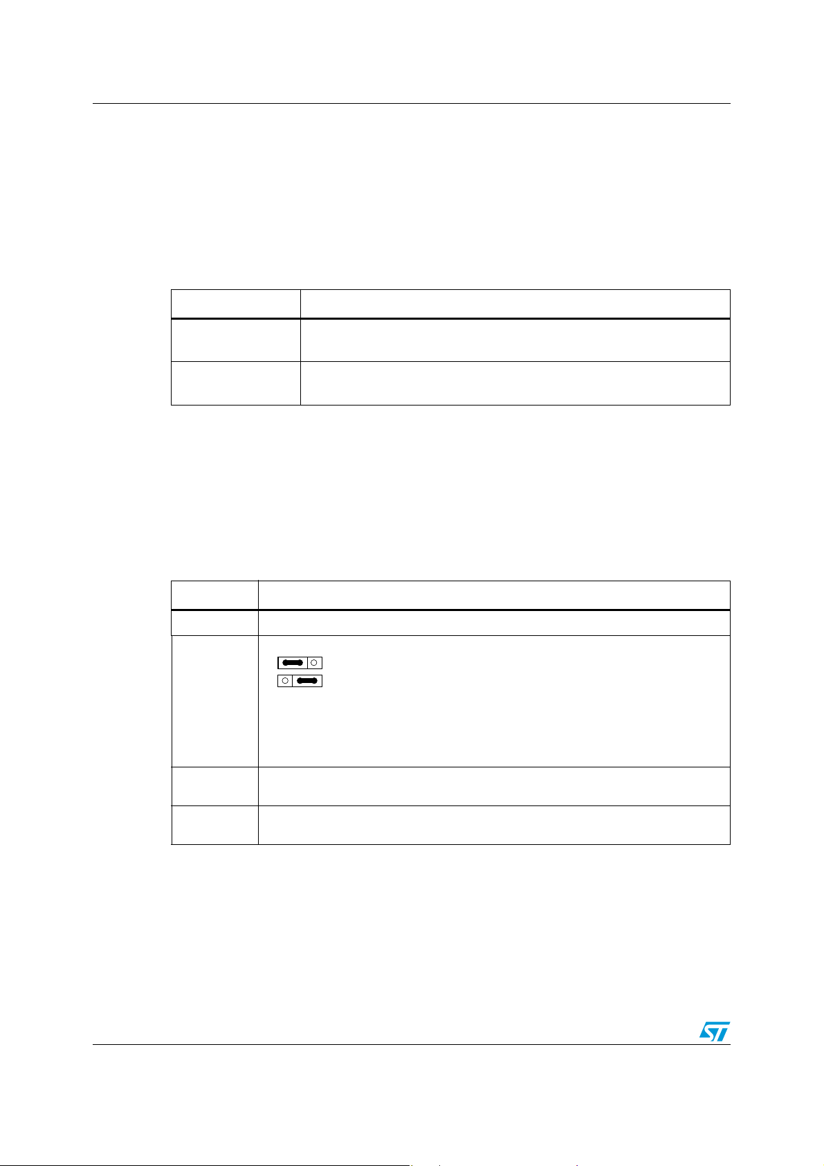
Table 2. Evaluation board connectors
Connector Description
P1
P2
P10
P20
Pow er connector (V
Standby control connector:
`
– pins 1 and 2 are shorted, TS488 operation mode, TS489 standby mode
123
`
– pins 2 and 3 are shorted, TS488 standby mode, TS489 operation mode
123
The connector pins are as follows:
–1: V
CC
– 2: Standby control
–3: GND
Input signal connector (GND and active input signal). The pin 1 and 2 for the input 1
and the pin 3 and 4 for the input 2
Output signal connector (GND and active output signal). The pin 1 and 2 for the
output 1 and the pin 3 and 4 for the output 2
and GND). Power supply voltage from 2.2V to 5.5V
CC
Caution: When you apply the power supply through P1, do not invert the polarity because it would
destroy the amplifier at U1.
2/5
Page 3

AN2621
Figure 1. Schematic diagram
P1
1
2
Vcc
VCC
C12
R12
20k
VCC
Jumper J1
330nF
P10
Input
Table 3. Component list for the evaluation board
Input1
1
2
3
Input2
4
C11
330nF
C21
VCC
P2
1
2
3
U1
20k
R11
20k
R21
C3
1uF
2
VIN1
5
STDB
3
BPS
6
VIN2
R22
20k
C22
Designation Quantity Description
C11, C21 2 330nF/16V, ceramic capacitors, 0805
C12, C22 0 Not assembled, 0603
C2 1 100nF/16V, ceramic capacitors, 0805
BIAS
8
Vcc
TS488=STDB
TS489=STDB
GND
4
1uFC1100nF
1
VOUT1
7
VOUT2
C2
R13
1k
220uF
C13
220uF
C23
R23
1k
OUT1
OUT2
P20
1
2
3
4
Output
C1, C3 2 1μF/50V, electrolytic capacitor, 1206
C13, C23 2 220μF/10V, electrolytic capacitor
P1 1 2-pin header 2.54mm pitch
P2 1 3-pin header 2.54mm pitch
P10, P20 2 4-pin header 2.54mm pitch
J1 1 Jumper, 2.54mm pitch
U1 1 TS488 or TS489
3/5
Page 4

2 Evaluation board layout
The following schematics show the layers and the top view of the evaluation board.
Figure 2. PCB top layer Figure 3. PCB bottom layer
AN2621
Figure 4. Top view of evaluation board
3 Revision history
Table 4. Document revision history
Date Revision Changes
25-Sep-2007 1 Initial release.
4/5
Page 5

AN2621
Please Read Carefully:
Information in this document is provided solely in connection with ST products. STMicroelectronics NV and its subsidiaries (“ST”) reserve the
right to make changes, corrections, modifications or improvements, to this document, and the products and services described herein at any
time, without notice.
All ST products are sold pursuant to ST’s terms and conditions of sal e.
Purchasers are solely res ponsibl e fo r the c hoic e, se lecti on an d use o f the S T prod ucts and s ervi ces d escr ibed he rein , and ST as sumes no
liability whatsoever relati ng to the choice, selection or use of the ST products and services described herein.
No license, express or implied, by estoppel or otherwise, to any intellectual property rights is granted under this document. If any part of this
document refers to any third pa rty p ro duc ts or se rv ices it sh all n ot be deem ed a lice ns e gr ant by ST fo r t he use of su ch thi r d party products
or services, or any intellectua l property c ontained the rein or consi dered as a warr anty coverin g the use in any manner whats oever of suc h
third party products or servi ces or any intellectual property contained therein.
UNLESS OTHERWISE SET FORTH IN ST’S TERMS AND CONDITIONS OF SALE ST DISCLAIMS ANY EXPRESS OR IMPLIED
WARRANTY WITH RESPECT TO THE USE AND/OR SALE OF ST PRODUCTS INCLUDING WITHOUT LIMITATION IMPLIED
WARRANTIES OF MERCHANTABILITY, FITNESS FOR A PARTICUL AR PURPOS E (AND THEIR EQUIVALE NTS UNDER THE LAWS
OF ANY JURISDICTION), OR INFRINGEMENT OF ANY PATENT, COPYRIGHT OR OTHER INTELLECTUAL PROPERTY RIGHT.
UNLESS EXPRESSLY APPROVED IN WRITING BY AN AUTHORIZED ST REPRESENTATIVE, ST PRODUCTS ARE NOT
RECOMMENDED, AUTHORIZED OR WARRANTED FOR USE IN MILITARY, AIR CRAFT, SPACE, LIFE SAVING, OR LIFE SUSTAINING
APPLICATIONS, NOR IN PRODUCTS OR SYSTEMS WHERE FAILURE OR MALFUNCTION MAY RESULT IN PERSONAL INJ URY,
DEATH, OR SEVERE PROPERTY OR ENVIRONMENTAL DAMAGE. ST PRODUCTS WHICH ARE NOT SPECIFIED AS "AUTOMOTIVE
GRADE" MAY ONLY BE USED IN AUTOMOTIVE APPLICATIONS AT USER’S OWN RISK.
Resale of ST products with provisions different from the statements and/or technical features set forth in this document shall immediately void
any warranty granted by ST fo r the ST pro duct or serv ice describe d herein and shall not cr eate or exten d in any manne r whatsoever , any
liability of ST.
ST and the ST logo are trademarks or registered trademarks of ST in various countries.
Information in this document su persedes and replaces all info rmation previously supplied.
The ST logo is a registered trademark of STMicroelectronics. All other names are the property of their respective owners.
© 2007 STMicroelectronics - All rights reserved
STMicroelectronics group of compan ie s
Australia - Belgium - Brazil - Canada - China - Czech Republic - Finland - France - Germany - Hong Kong - India - Israel - Italy - Japan -
Malaysia - Malta - Morocco - Singapore - Spain - Sweden - Switzerland - United Kingdom - United States of America
www.st.com
5/5
 Loading...