

Page 1
AN2620
Application note
3 A high-frequency synchronous 900 kHz
step-down converter based on the ST1S10
Introduction
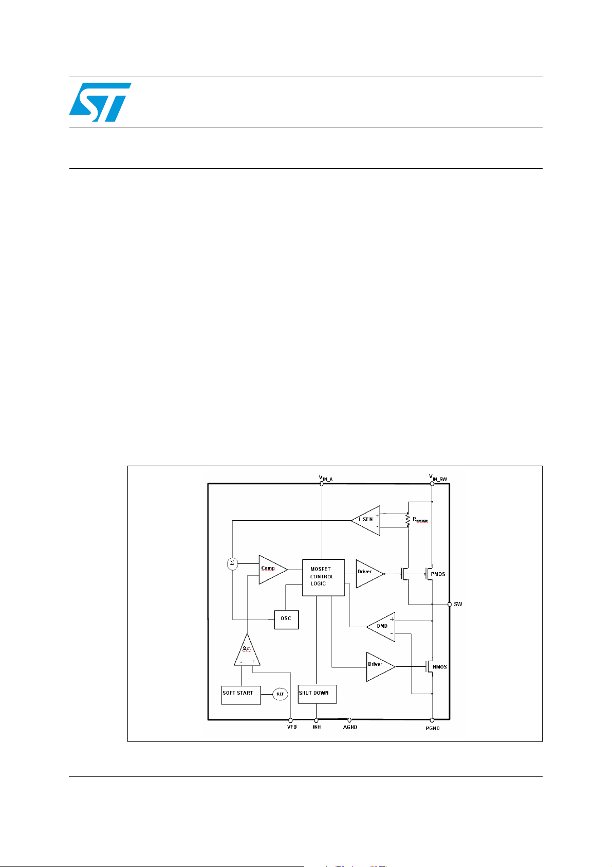
The ST1S10 is a step-down DC-DC converter with an optimized inhibit function for powering
high-voltage LCD applications and low-voltage digital core HDD applications. Generally, it
replaces the high current linear solution when high power dissipation is a problem. It
provides up to 3 A over an input voltage range of 2.5 V to 18 V and synchronous rectification
saves the external Schottky diode. A high internal switching frequency (0.9 MHz) allows it to
use tiny surface-mount components, as well as the resistor divider, to set the output voltage
value. Only an inductor and 3 capacitors are required. The current PWM mode architecture
and stable operation with low E.S.R SMD ceramic capacitors results in low, predictable
output ripple. To maximize the power conversion efficiency in light load, the regulator can
work in burst mode automatically. The device can operate in PWM mode at a fixed
frequency or synchronized to an external frequency. It switches at a frequency of 900 kHz
when SYNC is connected to ground or a fixed voltage (less than 5.5 V) and synchronizes
the switching frequency between 400 kHz to 1.2 MHz from the external clock that is applied
to SYNC. A thermal shutdown circuit is integrated and activates at 150 °C. Cycle-by-cycle
current limitation provides protection against shorted outputs. The on-chip 260 µs power-on
reset ensures the proper operation when switching on the power supply. The quiescent
current is less than 6 µA in the inhibit state. The device is available in MLP4x4 and SO-8
ePad packages.
Figure 1. Simplified schematic
May 2010 Doc ID 13883 Rev 3 1/20
www.st.com
Page 2

Contents AN2620
Contents
1 Application information component selection . . . . . . . . . . . . . . . . . . . . 4
1.1 Input capacitor . . . . . . . . . . . . . . . . . . . . . . . . . . . . . . . . . . . . . . . . . . . . . . 4
1.2 Output capacitor . . . . . . . . . . . . . . . . . . . . . . . . . . . . . . . . . . . . . . . . . . . . . 5
1.3 Inductor . . . . . . . . . . . . . . . . . . . . . . . . . . . . . . . . . . . . . . . . . . . . . . . . . . . 6
2 Thermal considerations . . . . . . . . . . . . . . . . . . . . . . . . . . . . . . . . . . . . . . 7
3 Short-circuit protection . . . . . . . . . . . . . . . . . . . . . . . . . . . . . . . . . . . . . . 8
4 Board usage recommendation . . . . . . . . . . . . . . . . . . . . . . . . . . . . . . . . . 9
4.1 External component selection for the ST1S10 demonstration board . . . . 13
4.2 Inductor selection . . . . . . . . . . . . . . . . . . . . . . . . . . . . . . . . . . . . . . . . . . . 13
4.3 Capacitors selection . . . . . . . . . . . . . . . . . . . . . . . . . . . . . . . . . . . . . . . . . 13
4.4 Heavy capacitive load condition . . . . . . . . . . . . . . . . . . . . . . . . . . . . . . . . 13
4.5 Low output voltage (Vout < 2.5 V) and 2.5 V < Vin < 8 V . . . . . . . . . . . . . 14
4.6 Layout considerations . . . . . . . . . . . . . . . . . . . . . . . . . . . . . . . . . . . . . . . . 16
5 Layout thermal considerations . . . . . . . . . . . . . . . . . . . . . . . . . . . . . . . 18
6 Revision history . . . . . . . . . . . . . . . . . . . . . . . . . . . . . . . . . . . . . . . . . . . 19
2/20 Doc ID 13883 Rev 3
Page 3

AN2620 List of figures
List of figures
Figure 1. Simplified schematic . . . . . . . . . . . . . . . . . . . . . . . . . . . . . . . . . . . . . . . . . . . . . . . . . . . . . . . 1
Figure 2. ST1S10 demonstration board typical diagram . . . . . . . . . . . . . . . . . . . . . . . . . . . . . . . . . . . 9
Figure 3. Demonstration board layout ST1S10 MLP package - top side . . . . . . . . . . . . . . . . . . . . . . 10
Figure 4. Demonstration board layout ST1S10 MLP package - bottom side . . . . . . . . . . . . . . . . . . . 10
Figure 5. Demonstration board layout ST1S10 SO-8 ePad - top side . . . . . . . . . . . . . . . . . . . . . . . . 11
Figure 6. Demonstration board layout ST1S10 SO-8 ePad package - bottom side. . . . . . . . . . . . . . 11
Figure 7. Enable jumper selection . . . . . . . . . . . . . . . . . . . . . . . . . . . . . . . . . . . . . . . . . . . . . . . . . . . 12
Figure 8. External synchronization. . . . . . . . . . . . . . . . . . . . . . . . . . . . . . . . . . . . . . . . . . . . . . . . . . . 12
Figure 9. ST1S10 application schematic for heavy capacitive load . . . . . . . . . . . . . . . . . . . . . . . . . . 14
Figure 10. ST1S10 application schematic for low output voltage (Vout < 2.5 V) and
2.5 V < Vin < 8 V. . . . . . . . . . . . . . . . . . . . . . . . . . . . . . . . . . . . . . . . . . . . . . . . . . . . . . . . . 14
Figure 11. ST1S10 application schematic for low output voltage (Vout < 2.5 V) and
8 V < Vin < 16 V . . . . . . . . . . . . . . . . . . . . . . . . . . . . . . . . . . . . . . . . . . . . . . . . . . . . . . . . . 15
Figure 12. PCB layout suggestion . . . . . . . . . . . . . . . . . . . . . . . . . . . . . . . . . . . . . . . . . . . . . . . . . . . . 16
Figure 13. PCB layout Vin_A and Vin_SW detail. . . . . . . . . . . . . . . . . . . . . . . . . . . . . . . . . . . . . . . . . 17
Figure 14. PCB layout details . . . . . . . . . . . . . . . . . . . . . . . . . . . . . . . . . . . . . . . . . . . . . . . . . . . . . . . 17
Doc ID 13883 Rev 3 3/20
Page 4

Application information component selection AN2620
1 Application information component selection
1.1 Input capacitor
The ST1S10 features two VIN pins: V
switching peak current is drawn, and V
drivers. The V
input capacitor reduces the current peaks drawn from the input power
IN_SW
for the power supply input voltage where the
IN_SW
to supply the ST1S10 internal circuitry and
IN_A
supply and reduces switching noise in the IC. High power supply source impedance requires
larger input capacitance.
For the V
input capacitor the RMS current rating is a critical parameter that must be
IN_SW
higher than the RMS input current. The maximum RMS input current can be calculated
using the following equation:
Equation 1
2
2D
I
RMSIO
⋅
D
-------------- -–
η
where η is the expected system efficiency, D is the duty cycle and I
2
D
------ -+⋅=
η
the output DC current.
O
This function reaches its maximum value at D = 0.5 and the equivalent RMS current is equal
to IO divided by 2 (considering η= 1).
The maximum and minimum duty cycles are:
Equation 2
V
+
outVF
D
MAX
-----------------------------------=
V
–
inMINVSW
Equation 3
V
+
D
MIN
outVF
-------------------------------------=
V
–
inMAXVSW
where V
internal PDMOS. Considering the range D
I
RMS
A minimum value of 4.7 µF for the V
is the voltage drop across the internal NMOS and VSW the voltage drop across the
F
MIN
to D
following through the input capacitor.
and a 0.1 µF ceramic capacitor for the V
IN_SW
suitable in most application conditions. A 10 µF or higher ceramic capacitor for the V
and a 1 µF (V
) are advisable in case of higher power supply source impedance or where
IN_A
it is needed to have long wires between the power supply source and the V
above suggested higher input capacitors values are also advisable in case of high output
capacitive load which can impact the switching peak current drawn from the input capacitor
during the startup transient.
It is also advisable to use ceramic capacitors with a voltage rating in the range of 1.5 times
the maximum input voltage. The input capacitors should be located as close as possible to
the V
IN
pins.
Different capacitors can be considered:
● Electrolytic capacitors. These are the most commonly used because they are the least
expensive and are available with a wide range of RMS current ratings. The only
4/20 Doc ID 13883 Rev 3
it is possible to determine the max
MAX
pins. The
IN
IN_A
IN_SW
are
Page 5

AN2620 Application information component selection
drawback is that, considering a requested ripple current rating, they are physically
larger than other capacitors.
● Ceramic capacitors. If available for the requested value and voltage rating, these
capacitors usually have a higher RMS current rating for a given physical dimension
(due to the very low ESR). The drawback is the quite high cost.
● Tantalum capacitor. Very good tantalum capacitors are becoming available, with very
low ESR and small size. The only problem is that they occasionally can burn if
subjected to very high current during the charge. So, it is better to avoid this type of
capacitor for the input filter of the device. In fact, they can be subjected to high surge
current when connected to the power supply.
1.2 Output capacitor
The output capacitor is very important in satisfying the output voltage ripple requirement.
Using a small inductor value to reduce the size of the choke is useful, but increases the
current ripple. So, to reduce the output voltage ripple, a low ESR capacitor is required.
The most important parameters for the output capacitor are the capacitance, the ESR and
the voltage rating.
The capacitance and the ESR affect the control loop stability, the output ripple voltage, and
transient response of the regulator. The ripple due to the capacitance can be calculated by
the following formula:
Equation 4
0.125 ΔISW⋅
-------------------------------- -=
F
SCout
⋅
where F
V
ripple C()
is the PWM switching frequency and ΔISW is the inductor peak-to-peak switching
S
current that can be calculated as:
Equation 5
VinV
–()
ΔI
SW
------------------------------
out
F
S
D⋅=
L⋅
where D is the duty cycle while the ripple due to the ESR is given by:
Equation 6
V
ripple ESR()ISw
Δ ESR⋅=
Use the above equations to define capacitor selection range, but final values should be
verified by testing an evaluation circuit.
Lower ESR ceramic capacitors are usually advisable to reduce the output ripple voltage.
Capacitors with higher voltage ratings have lower ESR values, providing lower output ripple
voltage.
Also the capacitor ESL value impacts the output ripple voltage, but ceramic capacitors
usually have very low ESL, making ripple voltages due to the ESL negligible. In order to
reduce ripple voltages due to a parasitic inductive effect, keep the output capacitor
connection paths as short as possible.
Doc ID 13883 Rev 3 5/20
Page 6

Application information component selection AN2620
The ST1S10 has been designed to have the best performances with ceramic capacitors. In
typical application conditions a minimum value of 22 µF ceramic capacitor is suggested on
the output, but higher values are suitable considering that the control loop has been
designed to properly work with a natural output LC frequency given by a 3.3 µH inductor and
22 µF output capacitor in the typical application (V
=12 V, V
in
out
=5 V).
It is advisable to use ceramic capacitors with a voltage rating in the range of 1.5 times the
maximum output voltage.
1.3 Inductor
The inductor value is very important because it fixes the ripple current flowing through the
output capacitor. The ripple current is usually fixed at 20-40% of I
I
= 3 A. The inductor value is approximately obtained by the following formula:
Omax
Equation 7
–
V
inVout
L
-------------------------
T
⋅=
IΔ
on
, that is 0.6-1.2 A with
Omax
where, T
For example, with V
is the ON time of the internal switch, given by D · T.
on
= 3.3 V, Vin = 5 V and ΔIO = 0.45 A, the inductor value is about
out
2.8 µH. The peak current thought the inductor is given by:
Equation 8
IΔ
I
I
PKIO
---- -+=
2
≥
SATIPK
It can be seen that if the inductor value decreases, the peak current (that has to be lower
than the current limit of the device) increases. So, for fixed the peak current, a higher value
of the inductor allows a higher value for the output current.
The ST1S10 is designed to have maximum performance with a 3.3 µH inductor value at
900 kHz.
The peak inductor current must be designed in order to not exceed the switching current
limit.
6/20 Doc ID 13883 Rev 3
Page 7

AN2620 Thermal considerations
2 Thermal considerations
The dissipated power of the device is related to three different sources:
● Switch losses due to the non-negligible R
Equation 9
P
ONP
R
DS on()P
-
Equation 10
P
ONN
R
DS on()N
-
where, D is the duty cycle of the application. Note that the duty cycle is theoretically
given by the ratio between V
and Vin, but in practical terms is quite higher than this
out
value to compensate the losses of the overall application. Due to this reason, the switch
losses related to the R
● Switch losses due to its turn-on and off. These are given by the following relationship:
increase compared to the ideal case.
DS(on)
Equation 11
. These are equal to:
DS(on)
2
I
D⋅⋅=
out
-
2
I
1D–()⋅⋅=
out
-
where T
and T
on
are the overlap times of the voltage across the power switch and the
off
current flowing into it during the turn-on and turn-off phases. T
time (typ. 30 ns).
● Quiescent current losses
Equation 12
PQVinIQ⋅=
where I
is the quiescent current.
Q
The junction temperature of device is:
Equation 13
where T
T
JTA
is the ambient temperature and Rth
A
Rth
J-A
P
⋅+=
JA–
TOT
is the thermal resistance junction-to-
ambient.
is the equivalent switching
SW
Doc ID 13883 Rev 3 7/20
Page 8

Short-circuit protection AN2620
3 Short-circuit protection
In short condition, the ST1S10 has two short protection functions to avoid a damaged
device.
● Overcurrent protection (OCP). The ST1S10 DC-DC converter is provided with a switch
overcurrent protection. If the switch current limit is reached, in order to protect the
application and the internal power switches and bonding wires, the device is
immediately shut down and kept in this condition for a T
and turns on again for a T
period (T
on
= 22 µs typ with typical application conditions).
on
This operation is repeated cycle by cycle. Normal operation is resumed when no
overcurrent is detected.
● Overvoltage protection (OVP). In order to protect the whole application and reduce the
total power dissipation during an overload or an output short-circuit condition, the
device is provided with a dynamic short-circuit protection which works by internally
monitoring the V
V
voltage is reduced causing the feedback voltage (VFB) to drop below 0.3 V typ,
OUT
the device goes in shutdown for T
period (T
= 130 µs typ). This operation is repeated cycle by cycle. Normal operation is
on
resumed when no overload is detected (V
(feedback voltage). In case of overload or output short-circuit, if the
FB
time (T
off
= 288 µs typ) and turns on again for a Ton
off
> 0.3 V typ) for a full Ton period. This
FB
dynamic operation can greatly reduce the power dissipation in overload condition, still
ensuring excellent power-on startup, in most conditions.
period time (T
off
= 135 µs typ)
off
8/20 Doc ID 13883 Rev 3
Page 9

AN2620 Board usage recommendation
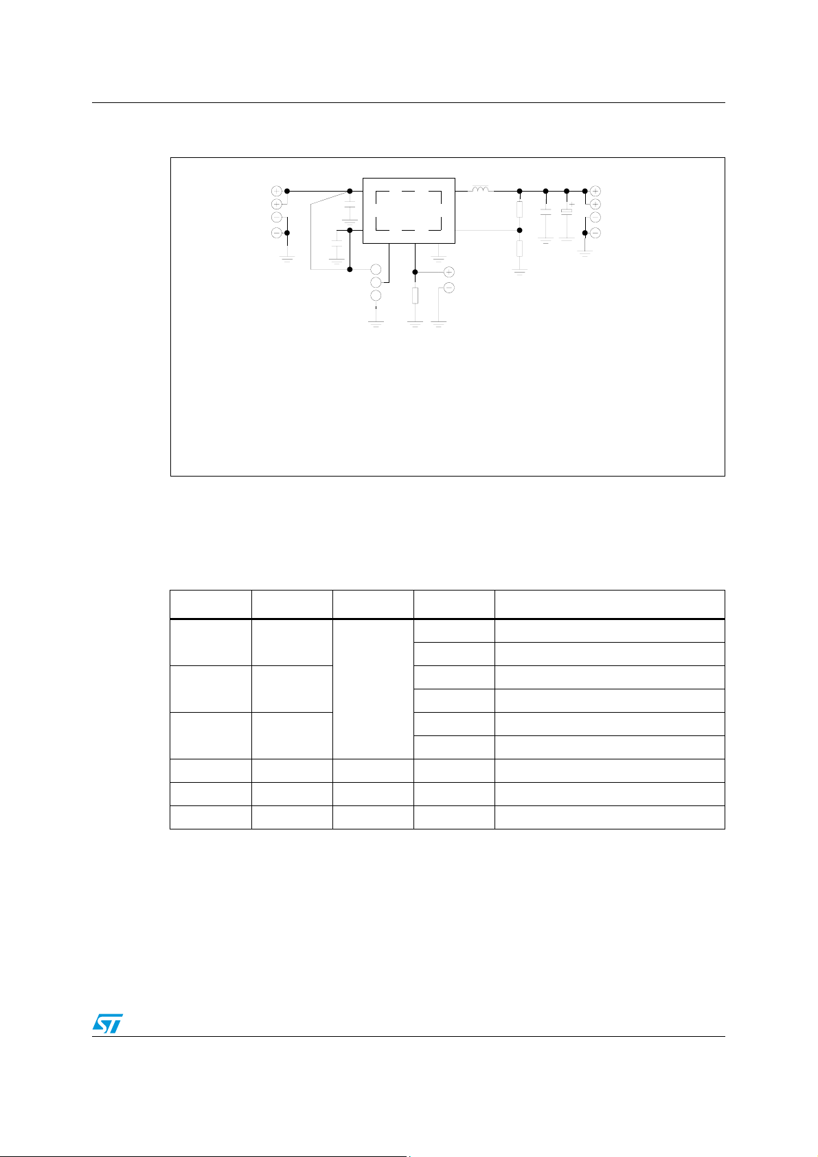
4 Board usage recommendation
The board shown in Figure 2 is provided with a Kelvin connection which means that for each
pin two lines are available, one used to supply or sink current and the other one used to
perform the needed measurement.
The ST1S10 inhibit pin should be connected to GND or V
, by a jumper, in order to turn off
in
or on the device.
If the SYNC pin is not used, it is better to connect to GND to avoid input noise to the device.
Figure 2. ST1S10 demonstration board typical diagram
12Vin
Vin
Vin
GND
GND
C1
C3
IC1
6
ePad*
1
2 5 4-8
L1
7
R1
3
C2
5Vout
Vout
Vout
GND
GND
R2
1
1-2=INH-ON
2-3=INH-OFF
R1=10 kΩ
R2=2 kΩ
R3=10 kΩ
2
3
R3
C1=4.7µF
C2=22µF
C3=0.1µF
SYNC
L1=3.3 µH
IC1=ST1S10
*ePad Connected to GND
Doc ID 13883 Rev 3 9/20
Page 10

Board usage recommendation AN2620
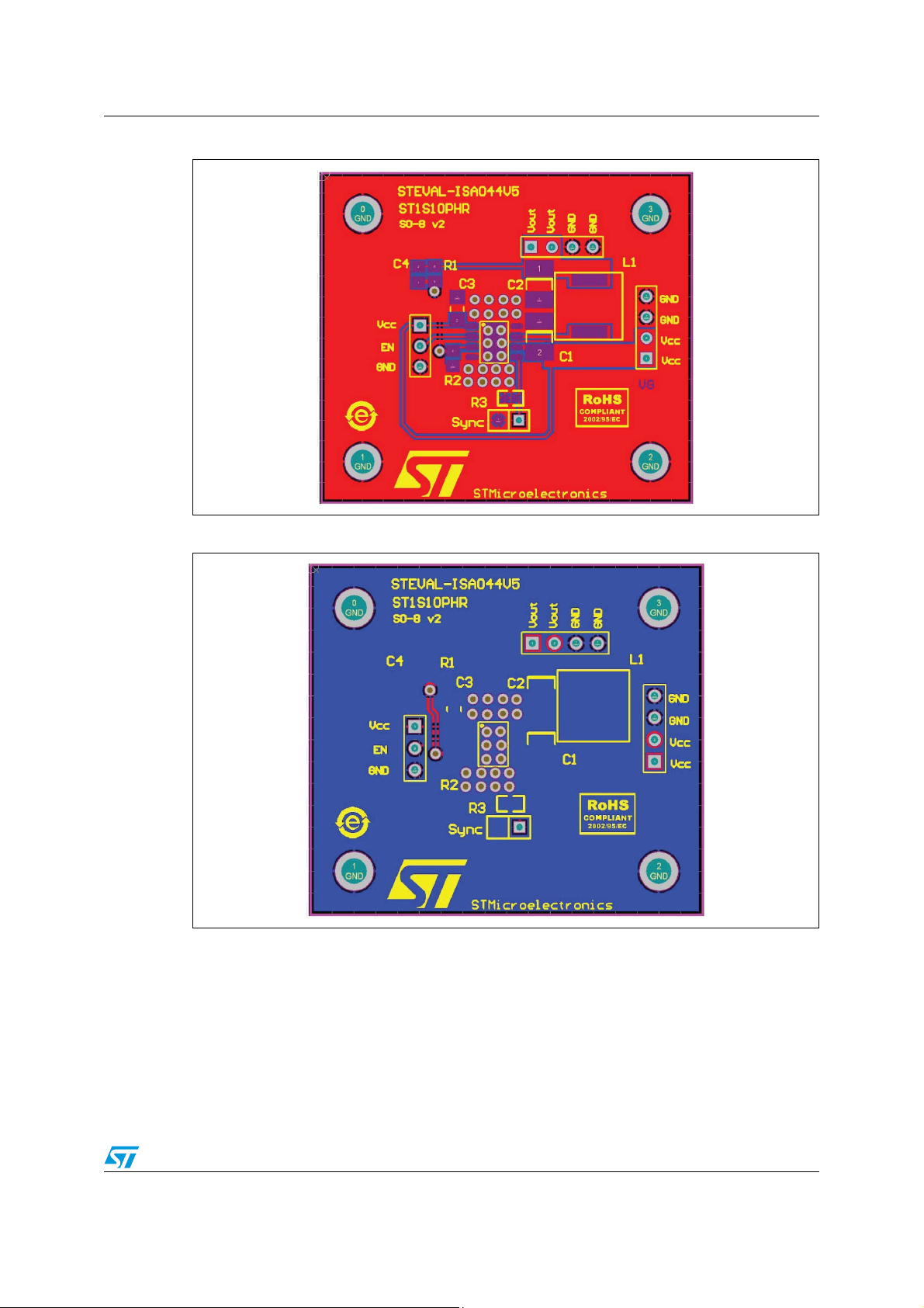
Figure 3. Demonstration board layout ST1S10 MLP package - top side
Figure 4. Demonstration board layout ST1S10 MLP package - bottom side
10/20 Doc ID 13883 Rev 3
Page 11
AN2620 Board usage recommendation
Figure 5. Demonstration board layout ST1S10 SO-8 ePad - top side
Figure 6. Demonstration board layout ST1S10 SO-8 ePad package - bottom side
Doc ID 13883 Rev 3 11/20
Page 12

Board usage recommendation AN2620
Figure 7. Enable jumper selection
Figure 8. External synchronization
12/20 Doc ID 13883 Rev 3
Page 13

AN2620 Board usage recommendation
4.1 External component selection for the ST1S10 demonstration board
Figure 2 shows the typical application used to obtain an output voltage of 5 V.
In order to obtain the needed output voltage we must choose the resistor divider according
to the following formula:
Equation 14
V
outVFB
R1
1
------- -+⋅=
R2
where V
= 0.8 V and R2 suggested value is ~2 kΩ.
FB
4.2 Inductor selection
Due to the high frequency (900 kHz) it is possible to use a very small inductor value.
We tested our device with an inductor value of 3.3 µH with very good efficiency
performances.
As the device is able to provide an operative output current of 3 A, we strongly recommend
using inductors able to manage at least 4.4 A.
4.3 Capacitors selection
It is possible to use any X5R or X7R ceramic capacitor
● C1 = 4.7 µF (ceramic) or higher
● C2 = 22 µF (ceramic) or higher, ESR=10 ~ 100 mΩ range
● C3 = 0.1 µF (ceramic) or higher
It is possible to put several capacitors in parallel in order to reduce the equivalent series
resistor and improve the ripple present in the output voltage.
4.4 Heavy capacitive load condition
Thanks to the OCP and OVP circuit, the ST1S10 is strongly protected against short-circuit
and overload damages. However, a highly capacitive load on the output may cause a difficult
startup. This can be solved by using the modified application circuit shown in Figure 9 in
which a minimum of 10 µF for C1 and a 4.7 µF ceramic capacitor for C3 are used. Moreover,
for C
divider resistor (R1) as shown in Figure 9. The suggested value for C4 is 4.7 nF ~ 47 nF.
Note that the C4 may impact the control loop response and should be added only when a
capacitive load higher than 100 µF is present at all times. If the high capacitive load is
variable or not present at any time, in addition to C4 it is advisable to increase the output
ceramic capacitor C2 from 22 µF to 47 µF (or use 2 x 22 µF capacitors in parallel). Also in
this case it is advisable to further increase the input capacitors with a minimum of 10 µF for
C1 and a 4.7 µF ceramic capacitor for C3 as shown in Figure 10.
>100 µF, it is needed to add the C4 capacitor in parallel to the upper voltage
LOAD
Doc ID 13883 Rev 3 13/20
Page 14

Board usage recommendation AN2620
Figure 9. ST1S10 application schematic for heavy capacitive load
IC1
12 V
12 V
V
V
IN
IN
V
V
IN
IN
GND
GND
GND
GND
1-2 = INH-ON
1-2 = INH-ON
2-3 = INH-OFF
2-3 = INH-OFF
R1 = 100 kΩ
R1 = 100 kΩ
R2 = 20 kΩ
R2 = 20 kΩ
R3 = 10 kΩ
R3 = 10 kΩ
IN
IN
C3
C3
C1
C1
C1 = 4.7 µF
C1 = 4.7 µF
C2 = 22 µF
C2 = 22 µF
C3 = 0.1~4.7 µF
C3 = 0.1~4.7 µF
C4 = 4.7 nF
C4 = 4.7 nF
IC1
6
6
ePad*
ePad*
1
1
254-8
254-8
1
1
2
2
R3
R3
3
3
L1
L1
7
7
R1
R1
3
3
R2
R2
SYNC
SYNC
L1 = 3.3 µH
L1 = 3.3 µH
IC1 = ST1S10
IC1 = ST1S10
*ePad Connected to GND
*ePad Connected to GND
C4
C4
C2
C2
5 V
5 V
OUT
OUT
V
V
OUT
OUT
V
V
OUT
OUT
GND
GND
GND
GND
4.5 Low output voltage (V
For applications with lower output voltage levels (V
the inductor values should be selected in a way that improves the DC-DC control loop
behavior.
In this output condition two cases must be considered: V
For V
shown in Figure 10.
For V
the 2 x 22 µF output capacitors as shown in Figure 11.
Figure 10. ST1S10 application schematic for low output voltage (V
< 8 V the use of 2 x 22 µF capacitors in parallel to the output is recommended, as
in
> 8 V, a 100 µF electrolytic capacitor with ESR < 0.1 should be added in parallel to
in
2.5 V < V
8<Vin
Vin
< 8 V
in
C1
Vin
GND
GND
C3
1-2=INH-ON
2-3=INH-OFF
< 2.5 V) and 2.5 V < Vin < 8 V
out
< 2.5 V) the output capacitance and
out
> 8 V and Vin < 8 V.
in
IC1
6
ePad*
1
254-8
L1
7
R1
C2
3
R2
1
2
3
R3
SYNC
out
<2.5Vout
Vout
Vout
GND
GND
< 2.5 V) and
R1=*
Ω
R2=2 k
R3=10 k Ω
C1=2*4.7 µF or 10 µF
C2=2*22 µF
C3=0.47~1 µF
L1=2.2 µH to 1 µH
IC1=ST1S10
*ePad Connected to GND
14/20 Doc ID 13883 Rev 3
Page 15
AN2620 Board usage recommendation
Figure 11. ST1S10 application schematic for low output voltage (V
8 V < V
8<Vin<16V
Vin
Vin
GND
GND
< 16 V
in
C1
IC1
6
ePad*
C3
1
25
4-8
L1
<2.5Vout
7
C2
R1
C4
3
R2
< 2.5 V) and
out
Vout
Vout
GND
GND
1
1-2=INH-ON
2-3=INH-OFF
R1=*
R2=2 k Ω
R3=10 k Ω
2
3
R3
C1=2*4.7 µF or 10 µF
C2=2*22 µF
C3=4.7 µF
C4=100 µF el E.S.R.<0.1
SYNC
Ω
L1=2.2 µH to 1 µH
IC1=ST1S10
*ePad Connected to GND
C4 suggested component:
Panasonic aluminium electrolytic capacitor FM series, part number - EEUFM1H101
100 µF 50 V impedance = 0.061 Ω at 100 kHz 20 °C
Table 1. Bill of material with most commonly used components
Name Value Material Brand P/N
C1 4.7 µF
C2 22 µF
C3 0.1 µF
L 1 µH TDK RLF7030T-1R0N6R4
2.2 µH TDK RLF7030T-2R2M5R4
3.3 µH TDK RLF7030T-3R3M4R1
Ceramic
TDK C3216X7R1475K
muRata GRM21BR71A255KA12L
TDK C3225X7R1C226M
muRata GRM32ER61C226KE20L
TDK C1005X5R1E104K
muRata GRM319R71H104KA01
Doc ID 13883 Rev 3 15/20
Page 16

Board usage recommendation AN2620
4.6 Layout considerations
The layout is an important step in the design for all switching power supplies.
The high-speed operation (900 kHz) of the ST1S10 device demands careful attention to the
PCB layout. Care must be taken in the board layout to obtain maximum device performance,
otherwise the regulator could show poor line and load regulation, stability issues as well as
EMI problems.
It is critical to provide a low inductance, impedance ground path. Therefore, use wide and
short traces for the main current paths.
The input capacitor must be placed as close as possible to the IC pins as well as the
inductor and output capacitor. Use a common ground node for power ground and a different
one for control ground (AGND) to minimize the effects of ground noise. Connect these
ground nodes together underneath the device and make sure that small signal components
returning to the AGND pin do not share the high current path of C
The feedback voltage sense line (V
) should be connected right to the output capacitor and
FB
routed away from noisy components and traces (e.g., SW line). Its trace should be
minimized and shielded by a guard-ring connected to the ground.
Figure 12. PCB layout suggestion
and C
IN
OUT
.
Enable/
Enable/
Disable
Disable
VFBguard-ring
VFBguard-ring
Output Voltage
Output Voltage
Input Sync
Input Sync
Input capacitor C1 must be placed
Input capacitor C1 must be placed
as close as possible to the IC
as close as possible to the IC
pins as well as the inductor L1
pins as well as the inductor L1
and Output capacitor C2
and Output capacitor C2
Input Power Supply
Input Power Supply
Via holes from thermal pad
Via holes from thermal pad
To bottom layer
To bottom layer
16/20 Doc ID 13883 Rev 3
Page 17

AN2620 Board usage recommendation
Figure 13. PCB layout Vin_A and Vin_SW detail
Trace to pin 6 (Vin_SW)
Trace to pin 6 (Vin_SW)
must be thick
must be thick
(high current)
(high current)
The trace connecting pin 1 (Vin_A) and pin 2 (EN) to input supply
The trace connecting pin 1 (Vin_A) and pin 2 (EN) to input supply
should start very close to pin 6 (Vin_SW) to minimize voltage drop
should start very close to pin 6 (Vin_SW) to minimize voltage drop
Figure 14. PCB layout details
Equation 15
I
INIPOWERGROUNDIOUTIDEVICEIC1IC2
Doc ID 13883 Rev 3 17/20
+++==
Page 18

Layout thermal considerations AN2620
5 Layout thermal considerations
The leadframe die pad of the ST1S10 is exposed at the bottom of the package and must be
soldered directly to a properly designed thermal pad on the PCB (ground copper area used
as a heat sink).
The addition of thermal vias from the thermal pad to an internal or bottom ground plane
helps to increase the power dissipation.
18/20 Doc ID 13883 Rev 3
Page 19

AN2620 Revision history
6 Revision history
Table 2. Document revision history
Date Revision Changes
20-Aug-2008 1 Initial release
04-Nov-2008 2 Title changed on cover page to improve readability
13-May-2010 3 Modified: Figure 9 on page 14, Figure 12 and Figure 13 on page 17
Doc ID 13883 Rev 3 19/20
Page 20

AN2620
Please Read Carefully:
Information in this document is provided solely in connection with ST products. STMicroelectronics NV and its subsidiaries (“ST”) reserve the
right to make changes, corrections, modifications or improvements, to this document, and the products and services described herein at any
time, without notice.
All ST products are sold pursuant to ST’s terms and conditions of sale.
Purchasers are solely responsible for the choice, selection and use of the ST products and services described herein, and ST assumes no
liability whatsoever relating to the choice, selection or use of the ST products and services described herein.
No license, express or implied, by estoppel or otherwise, to any intellectual property rights is granted under this document. If any part of this
document refers to any third party products or services it shall not be deemed a license grant by ST for the use of such third party products
or services, or any intellectual property contained therein or considered as a warranty covering the use in any manner whatsoever of such
third party products or services or any intellectual property contained therein.
UNLESS OTHERWISE SET FORTH IN ST’S TERMS AND CONDITIONS OF SALE ST DISCLAIMS ANY EXPRESS OR IMPLIED
WARRANTY WITH RESPECT TO THE USE AND/OR SALE OF ST PRODUCTS INCLUDING WITHOUT LIMITATION IMPLIED
WARRANTIES OF MERCHANTABILITY, FITNESS FOR A PARTICULAR PURPOSE (AND THEIR EQUIVALENTS UNDER THE LAWS
OF ANY JURISDICTION), OR INFRINGEMENT OF ANY PATENT, COPYRIGHT OR OTHER INTELLECTUAL PROPERTY RIGHT.
UNLESS EXPRESSLY APPROVED IN WRITING BY AN AUTHORIZED ST REPRESENTATIVE, ST PRODUCTS ARE NOT
RECOMMENDED, AUTHORIZED OR WARRANTED FOR USE IN MILITARY, AIR CRAFT, SPACE, LIFE SAVING, OR LIFE SUSTAINING
APPLICATIONS, NOR IN PRODUCTS OR SYSTEMS WHERE FAILURE OR MALFUNCTION MAY RESULT IN PERSONAL INJURY,
DEATH, OR SEVERE PROPERTY OR ENVIRONMENTAL DAMAGE. ST PRODUCTS WHICH ARE NOT SPECIFIED AS "AUTOMOTIVE
GRADE" MAY ONLY BE USED IN AUTOMOTIVE APPLICATIONS AT USER’S OWN RISK.
Resale of ST products with provisions different from the statements and/or technical features set forth in this document shall immediately void
any warranty granted by ST for the ST product or service described herein and shall not create or extend in any manner whatsoever, any
liability of ST.
ST and the ST logo are trademarks or registered trademarks of ST in various countries.
Information in this document supersedes and replaces all information previously supplied.
The ST logo is a registered trademark of STMicroelectronics. All other names are the property of their respective owners.
© 2010 STMicroelectronics - All rights reserved
STMicroelectronics group of companies
Australia - Belgium - Brazil - Canada - China - Czech Republic - Finland - France - Germany - Hong Kong - India - Israel - Italy - Japan -
Malaysia - Malta - Morocco - Philippines - Singapore - Spain - Sweden - Switzerland - United Kingdom - United States of America
www.st.com
20/20 Doc ID 13883 Rev 3
 Loading...