

Page 1
AN2606
Application note
STM32™ microcontroller system memory boot mode
Introduction
The bootloader is stored in the internal boot ROM memory (system memory) of STM32
devices. It is programmed by ST during production. Its main task is to download the
application program to the internal Flash memory through one of the available serial
peripherals (USART, CAN, USB, etc.). A communication protocol is defined for each serial
interface, with a compatible command set and sequences.
This document applies to the products listed in Ta b le 1 . They will be referred to STM32
throughout the document.
Table 1. Application products
Type Part number or product series
STM32F051x6, STM32F051x8
STM32 F1 Mainstream
Microcontroller
STM32 F2 Hi-performance
STM32F40xx and STM32F41xx
STM32L151xx, STM32F152xx, and
STM32F162xx
The main features of the bootloader are the following:
● It uses an embedded serial interface to download the code with a predefined
communication protocol
● It transfers and updates the Flash memory code, the data, and the vector table sections
This application note presents the general concept of the bootloader. It describes the
supported peripherals and hardware requirements to be considered when using the
bootloader of any STM32 device currently in production. However the specifications of the
low-level communication protocol for each supported serial peripheral are documented in
separate documents. For specifications of the USART protocol used in the bootloader
please refer to AN3155. For the specification of CAN protocol used in the bootloader please
refer to AN3154. For the specification of DFU (USB Device) protocol used in the bootloader
please refer to AN3156.
July 2012 Doc ID 13801 Rev 14 1/88
www.st.com
Page 2

Contents AN2606
Contents
1 Related documents . . . . . . . . . . . . . . . . . . . . . . . . . . . . . . . . . . . . . . . . . . 8
2 Glossary . . . . . . . . . . . . . . . . . . . . . . . . . . . . . . . . . . . . . . . . . . . . . . . . . . . 9
3 General bootloader description . . . . . . . . . . . . . . . . . . . . . . . . . . . . . . . 10
3.1 Bootloader activation . . . . . . . . . . . . . . . . . . . . . . . . . . . . . . . . . . . . . . . . 10
3.2 Exiting System memory boot mode . . . . . . . . . . . . . . . . . . . . . . . . . . . . . 10
3.3 Bootloader identification . . . . . . . . . . . . . . . . . . . . . . . . . . . . . . . . . . . . . . 11
4 STM32F100xx, STM32F101xx, STM32F102xx,
STM32F103xx, medium-density and
high-density value line bootloader . . . . . . . . . . . . . . . . . . . . . . . . . . . . 13
4.1 Bootloader configuration . . . . . . . . . . . . . . . . . . . . . . . . . . . . . . . . . . . . . 13
4.2 Bootloader hardware requirements . . . . . . . . . . . . . . . . . . . . . . . . . . . . . 14
4.3 Bootloader selection . . . . . . . . . . . . . . . . . . . . . . . . . . . . . . . . . . . . . . . . . 14
4.4 Bootloader version . . . . . . . . . . . . . . . . . . . . . . . . . . . . . . . . . . . . . . . . . . 15
5 STM32F105xx and STM32F107xx device bootloader . . . . . . . . . . . . . . 16
5.1 Bootloader configuration . . . . . . . . . . . . . . . . . . . . . . . . . . . . . . . . . . . . . 16
5.2 Bootloader hardware requirements . . . . . . . . . . . . . . . . . . . . . . . . . . . . . 18
5.3 Bootloader selection . . . . . . . . . . . . . . . . . . . . . . . . . . . . . . . . . . . . . . . . . 19
5.4 Bootloader version . . . . . . . . . . . . . . . . . . . . . . . . . . . . . . . . . . . . . . . . . . 21
5.4.1 How to identify STM32F105xx/107xx bootloader versions . . . . . . . . . . 21
5.4.2 Bootloader unavailability on STM32F105xx/STM32F107xx devices
with a date code below 937 . . . . . . . . . . . . . . . . . . . . . . . . . . . . . . . . . . 22
5.4.3 USART bootloader Get-Version command returns 0x20
instead of 0x22 . . . . . . . . . . . . . . . . . . . . . . . . . . . . . . . . . . . . . . . . . . . 22
5.4.4 PA9 excessive power consumption when USB cable is plugged
in bootloader V2.0 . . . . . . . . . . . . . . . . . . . . . . . . . . . . . . . . . . . . . . . . . 23
6 STM32F101xx and STM32F103xx XL-density device bootloader . . . . 24
6.1 Dual bank boot feature . . . . . . . . . . . . . . . . . . . . . . . . . . . . . . . . . . . . . . . 24
6.2 Bootloader configuration . . . . . . . . . . . . . . . . . . . . . . . . . . . . . . . . . . . . . 26
6.3 Bootloader hardware requirements . . . . . . . . . . . . . . . . . . . . . . . . . . . . . 27
2/88 Doc ID 13801 Rev 14
Page 3

AN2606 Contents
6.4 Bootloader selection . . . . . . . . . . . . . . . . . . . . . . . . . . . . . . . . . . . . . . . . . 28
6.5 Bootloader version . . . . . . . . . . . . . . . . . . . . . . . . . . . . . . . . . . . . . . . . . . 30
7 STM32L15xx Medium-density Ultralow power device bootloader . . . 31
7.1 Bootloader configuration . . . . . . . . . . . . . . . . . . . . . . . . . . . . . . . . . . . . . 31
7.2 Bootloader hardware requirements . . . . . . . . . . . . . . . . . . . . . . . . . . . . . 32
7.3 Bootloader selection . . . . . . . . . . . . . . . . . . . . . . . . . . . . . . . . . . . . . . . . . 32
7.4 Important considerations . . . . . . . . . . . . . . . . . . . . . . . . . . . . . . . . . . . . . 34
7.5 Bootloader version . . . . . . . . . . . . . . . . . . . . . . . . . . . . . . . . . . . . . . . . . . 35
8 STM32L15xx and STM32L16xx High-density ultralow power device
bootloader 36
8.1 Dual bank boot feature . . . . . . . . . . . . . . . . . . . . . . . . . . . . . . . . . . . . . . . 36
8.2 Bootloader configuration . . . . . . . . . . . . . . . . . . . . . . . . . . . . . . . . . . . . . 38
8.3 Bootloader hardware requirements . . . . . . . . . . . . . . . . . . . . . . . . . . . . . 41
8.4 Bootloader selection . . . . . . . . . . . . . . . . . . . . . . . . . . . . . . . . . . . . . . . . . 42
8.5 Important considerations . . . . . . . . . . . . . . . . . . . . . . . . . . . . . . . . . . . . . 44
8.6 Bootloader version . . . . . . . . . . . . . . . . . . . . . . . . . . . . . . . . . . . . . . . . . . 45
9 STM32F205/215xx, and STM32F207/217xx bootloader . . . . . . . . . . . . 46
9.1 Bootloader V2.x . . . . . . . . . . . . . . . . . . . . . . . . . . . . . . . . . . . . . . . . . . . . 46
9.1.1 Bootloader configuration . . . . . . . . . . . . . . . . . . . . . . . . . . . . . . . . . . . . 46
9.1.2 Bootloader hardware requirements . . . . . . . . . . . . . . . . . . . . . . . . . . . . 47
9.1.3 Bootloader selection . . . . . . . . . . . . . . . . . . . . . . . . . . . . . . . . . . . . . . . 48
9.1.4 Important considerations . . . . . . . . . . . . . . . . . . . . . . . . . . . . . . . . . . . . 50
9.1.5 Bootloader V2.x versions . . . . . . . . . . . . . . . . . . . . . . . . . . . . . . . . . . . . 51
9.2 Bootloader V3.x . . . . . . . . . . . . . . . . . . . . . . . . . . . . . . . . . . . . . . . . . . . . 52
9.2.1 Bootloader configuration . . . . . . . . . . . . . . . . . . . . . . . . . . . . . . . . . . . . 52
9.2.2 Bootloader hardware requirements . . . . . . . . . . . . . . . . . . . . . . . . . . . . 54
9.2.3 Bootloader selection . . . . . . . . . . . . . . . . . . . . . . . . . . . . . . . . . . . . . . . 56
9.2.4 Important considerations . . . . . . . . . . . . . . . . . . . . . . . . . . . . . . . . . . . . 59
9.2.5 Bootloader version V3.x . . . . . . . . . . . . . . . . . . . . . . . . . . . . . . . . . . . . . 60
10 STM32F405/415xx, and STM32F407/417xx bootloader . . . . . . . . . . . . 62
10.1 Bootloader configuration . . . . . . . . . . . . . . . . . . . . . . . . . . . . . . . . . . . . . 62
10.2 Bootloader hardware requirements . . . . . . . . . . . . . . . . . . . . . . . . . . . . . 64
Doc ID 13801 Rev 14 3/88
Page 4

Contents AN2606
10.3 Bootloader selection . . . . . . . . . . . . . . . . . . . . . . . . . . . . . . . . . . . . . . . . . 65
10.4 Important considerations . . . . . . . . . . . . . . . . . . . . . . . . . . . . . . . . . . . . . 68
10.5 Bootloader version . . . . . . . . . . . . . . . . . . . . . . . . . . . . . . . . . . . . . . . . . . 69
11 STM32F051x6 and STM32F051x8 device bootloader . . . . . . . . . . . . . . 71
11.1 Bootloader configuration . . . . . . . . . . . . . . . . . . . . . . . . . . . . . . . . . . . . . 71
11.2 Bootloader hardware requirements . . . . . . . . . . . . . . . . . . . . . . . . . . . . . 71
11.3 Bootloader selection . . . . . . . . . . . . . . . . . . . . . . . . . . . . . . . . . . . . . . . . . 72
11.4 Important considerations . . . . . . . . . . . . . . . . . . . . . . . . . . . . . . . . . . . . . 74
11.5 Bootloader version . . . . . . . . . . . . . . . . . . . . . . . . . . . . . . . . . . . . . . . . . . 74
12 Device-dependent bootloader parameters . . . . . . . . . . . . . . . . . . . . . . 75
13 Bootloader timing characteristics . . . . . . . . . . . . . . . . . . . . . . . . . . . . . 77
13.1 USART bootloader timing characteristics . . . . . . . . . . . . . . . . . . . . . . . . . 77
13.2 USB bootloader timing characteristics . . . . . . . . . . . . . . . . . . . . . . . . . . 82
14 Revision history . . . . . . . . . . . . . . . . . . . . . . . . . . . . . . . . . . . . . . . . . . . 85
4/88 Doc ID 13801 Rev 14
Page 5

AN2606 List of tables
List of tables
Table 1. Application products . . . . . . . . . . . . . . . . . . . . . . . . . . . . . . . . . . . . . . . . . . . . . . . . . . . . . . . 1
Table 2. Boot pin configuration . . . . . . . . . . . . . . . . . . . . . . . . . . . . . . . . . . . . . . . . . . . . . . . . . . . . . 10
Table 3. Embedded bootloaders. . . . . . . . . . . . . . . . . . . . . . . . . . . . . . . . . . . . . . . . . . . . . . . . . . . . 11
Table 4. STM32F10xxx configuration in System memory boot mode . . . . . . . . . . . . . . . . . . . . . . . 13
Table 5. STM32F10xxx bootloader versions . . . . . . . . . . . . . . . . . . . . . . . . . . . . . . . . . . . . . . . . . . 15
Table 6. STM32F105xx/107xx configuration in System memory boot mode . . . . . . . . . . . . . . . . . . 16
Table 7. STM32F105xx and STM32F107xx bootloader versions. . . . . . . . . . . . . . . . . . . . . . . . . . . 21
Table 8. Boot pin and BFB2 bit configuration . . . . . . . . . . . . . . . . . . . . . . . . . . . . . . . . . . . . . . . . . . 25
Table 9. STM32F10xxx XL-density configuration in System memory boot mode . . . . . . . . . . . . . . 26
Table 10. XL-density bootloader versions . . . . . . . . . . . . . . . . . . . . . . . . . . . . . . . . . . . . . . . . . . . . . 30
Table 11. STM32L15xxx configuration in System memory boot mode. . . . . . . . . . . . . . . . . . . . . . . . 31
Table 12. STM32L15xxx bootloader versions . . . . . . . . . . . . . . . . . . . . . . . . . . . . . . . . . . . . . . . . . . 35
Table 13. Boot pin and BFB2 bit configuration . . . . . . . . . . . . . . . . . . . . . . . . . . . . . . . . . . . . . . . . . . 37
Table 14. STM32L1xx High-density configuration in System memory boot mode . . . . . . . . . . . . . . . 39
Table 15. STM32L1xx High-density bootloader versions . . . . . . . . . . . . . . . . . . . . . . . . . . . . . . . . . . 45
Table 16. STM32F2xx configuration in System memory boot mode . . . . . . . . . . . . . . . . . . . . . . . . . 46
Table 17. STM32F2xx Voltage Range configuration using bootloader V2.x . . . . . . . . . . . . . . . . . . . 51
Table 18. STM32F2xx bootloader V2.x versions . . . . . . . . . . . . . . . . . . . . . . . . . . . . . . . . . . . . . . . . 51
Table 19. STM32F2xx configuration in System memory boot mode . . . . . . . . . . . . . . . . . . . . . . . . . 52
Table 20. STM32F2xx Voltage Range configuration using bootloader V3.x . . . . . . . . . . . . . . . . . . . 60
Table 21. STM32F2xx bootloader V3.x versions . . . . . . . . . . . . . . . . . . . . . . . . . . . . . . . . . . . . . . . . 61
Table 22. STM32F4xx configuration in System memory boot mode . . . . . . . . . . . . . . . . . . . . . . . . . 62
Table 23. STM32F4xx Voltage Range configuration using bootloader . . . . . . . . . . . . . . . . . . . . . . . 69
Table 24. STM32F4xx bootloader version . . . . . . . . . . . . . . . . . . . . . . . . . . . . . . . . . . . . . . . . . . . . . 70
Table 25. STM32F51xx configuration in System memory boot mode . . . . . . . . . . . . . . . . . . . . . . . . 71
Table 26. STM32F051xx bootloader versions . . . . . . . . . . . . . . . . . . . . . . . . . . . . . . . . . . . . . . . . . . 74
Table 27. Bootloader device-dependant parameters . . . . . . . . . . . . . . . . . . . . . . . . . . . . . . . . . . . . . 75
Table 28. USART bootloader timings for low/medium/high-density and
value line devices . . . . . . . . . . . . . . . . . . . . . . . . . . . . . . . . . . . . . . . . . . . . . . . . . . . . . . . . 78
Table 29. USART bootloader timings for XL-density line devices . . . . . . . . . . . . . . . . . . . . . . . . . . . 79
Table 30. USART bootloader timings for connectivity line devices (PA9 pin low) . . . . . . . . . . . . . . . 79
Table 31. USART bootloader timings for connectivity line devices (PA9 high). . . . . . . . . . . . . . . . . . 80
Table 32. USART bootloader timings for STM32L15xx medium-density
ultralow power devices . . . . . . . . . . . . . . . . . . . . . . . . . . . . . . . . . . . . . . . . . . . . . . . . . . . . 80
Table 33. USART bootloader timings for STM32L15xx high-density
ultralow power devices . . . . . . . . . . . . . . . . . . . . . . . . . . . . . . . . . . . . . . . . . . . . . . . . . . . . 80
Table 34. USART bootloader timings for STM32F205/215xx and
STM32F207/217xx devices . . . . . . . . . . . . . . . . . . . . . . . . . . . . . . . . . . . . . . . . . . . . . . . . 81
Table 35. USART bootloader timings for STM32F405/415xx and
STM32F407/417xx devices . . . . . . . . . . . . . . . . . . . . . . . . . . . . . . . . . . . . . . . . . . . . . . . . 81
Table 36. USART bootloader timings for STM32F051x6 and STM32F051x8 devices. . . . . . . . . . . . 82
Table 37. USB minimum timings for connectivity line devices . . . . . . . . . . . . . . . . . . . . . . . . . . . . . . 83
Table 38. USB minimum timings for STM32L15xx high-density
ultralow power devices . . . . . . . . . . . . . . . . . . . . . . . . . . . . . . . . . . . . . . . . . . . . . . . . . . . . 83
Table 39. USB minimum timings for STM32F205/215xx,
and STM32F207/217xx devices . . . . . . . . . . . . . . . . . . . . . . . . . . . . . . . . . . . . . . . . . . . . . 84
Table 40. USB minimum timings for STM32F405/415xx,
and STM32F407/417xx devices . . . . . . . . . . . . . . . . . . . . . . . . . . . . . . . . . . . . . . . . . . . . . 84
Doc ID 13801 Rev 14 5/88
Page 6

List of tables AN2606
Table 41. Document revision history . . . . . . . . . . . . . . . . . . . . . . . . . . . . . . . . . . . . . . . . . . . . . . . . . 85
6/88 Doc ID 13801 Rev 14
Page 7

AN2606 List of figures
List of figures
Figure 1. Bootloader for STM32F10xxx with USART1 . . . . . . . . . . . . . . . . . . . . . . . . . . . . . . . . . . . 14
Figure 2. Bootloader selection for STM32F105xx and STM32F107xx devices . . . . . . . . . . . . . . . . . 20
Figure 3. Bootloader selection for STM32F10xxx XL-density devices. . . . . . . . . . . . . . . . . . . . . . . . 29
Figure 4. Bootloader selection for STM32L15xxx devices . . . . . . . . . . . . . . . . . . . . . . . . . . . . . . . . . 33
Figure 5. Bootloader selection for STM32L1xx High-density devices . . . . . . . . . . . . . . . . . . . . . . . . 43
Figure 6. Bootloader V2.x selection for STM32F2xx . . . . . . . . . . . . . . . . . . . . . . . . . . . . . . . . . . . . . 49
Figure 7. Bootloader V3.x selection for STM32F2xx . . . . . . . . . . . . . . . . . . . . . . . . . . . . . . . . . . . . . 58
Figure 8. Bootloader selection for STM32F4xx . . . . . . . . . . . . . . . . . . . . . . . . . . . . . . . . . . . . . . . . . 67
Figure 9. Bootloader selection for STM32F051xx . . . . . . . . . . . . . . . . . . . . . . . . . . . . . . . . . . . . . . . 73
Figure 10. USART bootloader timing waveforms. . . . . . . . . . . . . . . . . . . . . . . . . . . . . . . . . . . . . . . . . 78
Figure 11. USB bootloader timing waveforms . . . . . . . . . . . . . . . . . . . . . . . . . . . . . . . . . . . . . . . . . . . 83
Doc ID 13801 Rev 14 7/88
Page 8

Related documents AN2606
1 Related documents
All the documents mentioned below are available from http://www.st.com:
● Datasheets
– Low, medium and high-density STM32F101xx and STM32F103xx datasheets
– Low, medium and high-density STM32F100xx and STM32F102xx datasheets
– STM32F105xx/107xx connectivity line datasheet
– XL-density STM32F101xx and STM32F103xx datasheets
– STM32L151xx and STM32F152xx datasheet
– STM32F162xx datasheet
– STM32F205xx STM32F207xx and STM32F215xx STM32F217xx datasheets
– STM32F405xx STM32F407xx and STM32F415xx STM32F417xx datasheets
– STM32F051x6 and STM32F051x8 devices datasheets
● Reference manuals
– STM32F101xx, STM32F102xx, STM32F103xx and STM32F105xx/107xx
reference manual (RM0008)
– Low, medium and high-density STM32F100xx value line reference manual
(RM0041)
– STM32L151xx, STM32L152xx, and STM32L162xx advanced ARM-based 32-bit
MCUs reference manual (RM0038)
– STM32F205xx, STM32F207xx, STM32F215xx and STM32F217xx advanced
ARM-based 32-bit MCUs reference manual (RM00033)
– STM32F405xx, STM32F407xx, STM32F415xx and STM32F417xx advanced
ARM-based 32-bit MCUs reference manual (RM00090)
– STM32F051xx advanced ARM-based 32-bit
● Flash programming manuals
– STM32F101xx, STM32F102xx, STM32F103xx and STM32F105xx/107xx Flash
programming manual (PM0042)
– Low, medium and high-density STM32F100xx value line Flash programming
manual (PM0063)
– XL-density STM32F101xx and STM32F103xx Flash programming manual
(PM0068)
– STM32L151xx, STM32L152xx, and STM32L162xx Flash programming manual
(PM0062)
– STM32F205xx, STM32F207xx, STM32F215xx and STM32F217xx Flash
programming manual (PM0059)
– STM32F405xx, STM32F407xx, STM32F415xx and STM32F417xx Flash
programming manual (PM0081)
8/88 Doc ID 13801 Rev 14
Page 9

AN2606 Glossary
2 Glossary
Low-density devices are STM32F101xx, STM32F102xx and STM32F103xx
microcontrollers where the Flash memory density ranges between 16 and 32 Kbytes.
Medium-density devices are STM32F101xx, STM32F102xx and STM32F103xx
microcontrollers where the Flash memory density ranges between 64 and 128 Kbytes.
High-density devices are STM32F101xx and STM32F103xx microcontrollers where the
Flash memory density ranges between 256 and 512 Kbytes.
Connectivity line devices are STM32F105xx and STM32F107xx microcontrollers.
Low-density value line devices are STM32F100xx microcontrollers where the Flash
memory density ranges between 16 and 32 Kbytes.
Medium-density value line devices are STM32F100xx microcontrollers where the Flash
memory density ranges between 64 and 128 Kbytes.
High-density value line devices are STM32F100xx microcontrollers where the Flash
memory density ranges between 256 and 5128 Kbytes.
XL-density devices are STM32F101xx and STM32F103xx microcontrollers where the
Flash memory density ranges between 768 Kbytes and 1 Mbyte.
Medium-density ultralow power devices are STM32L151xx and STM32L152xx
microcontrollers where the program memory density ranges between 64 and 128 Kbytes.
High-density ultralow power devices are STM32L151xx, STM32L152xx and
STM32L162xx microcontrollers where the program memory density size is 384 Kbytes
STM32F2xxx devices are STM32F215xx, STM32F205xx, STM32F207xx and
SMT32F217xx microcontrollers with a Flash memory density ranging from 128 to
1024 Kbytes.
STM32F4xxx devices are STM32F415xx, STM32F405xx, STM32F407xx and
SMT32F417xx microcontrollers with a Flash memory density ranging from 512 to
1024 Kbytes.
STM32F051xx devices are STM32F051x6, STM32F051x8 microcontrollers where the
Flash memory density ranges between 32 and 64 Kbytes.
Doc ID 13801 Rev 14 9/88
Page 10
General bootloader description AN2606
3 General bootloader description
3.1 Bootloader activation
The bootloader is automatically activated by configuring the BOOT0 and BOOT1 pins in the
specific “System memory” configuration (see Ta b l e 2) and then by applying a reset.
Depending on the used pin configuration, the Flash memory, system memory or SRAM is
selected as the boot space, as shown in Ta bl e 2 below.
In some products, BOOT1 is not an I/O but a bit in the option byte area. This is the case for
the STM32F05x devices where BOOT1 is configured through nBoot1 bit in the option bytes.
● When nBoot1 bit is set to 1, it corresponds to BOOT1 reset to 0 in Tab le 2
● When nBoot1 bit is reset to 0, it corresponds to BOOT1 set to 1 n Tab l e 2.
Table 2. Boot pin configuration
Boot mode selection pins
Boot mode Aliasing
BOOT1 BOOT0
X 0 User Flash memory User Flash memory is selected as the boot space
0 1 System memory System memory is selected as the boot space
1 1 Embedded SRAM Embedded SRAM is selected as the boot space
Ta bl e 2 shows that the STM32 microcontrollers enter System memory boot mode if the
BOOT pins are configured as follows:
● BOOT0 = 1
● BOOT1 = 0
The values on the BOOT pins are latched on the fourth rising edge of SYSCLK after a reset.
3.2 Exiting System memory boot mode
System memory boot mode must be exited in order to start execution of the application
program. This can be done by applying a hardware reset. During reset, the BOOT pins/bits
(BOOT0 and BOOT1) must be set at the proper levels to select the desired boot mode (see
Ta bl e 2 ). Following the reset, the CPU starts code execution from the boot memory located
at the bottom of the memory address space starting from 0x0000 0000.
10/88 Doc ID 13801 Rev 14
Page 11
AN2606 General bootloader description
3.3 Bootloader identification
Depending on the STM32 device used, the bootloader may support one or more embedded
serial peripherals used to download the code to the internal Flash memory. The bootloader
identifier (ID) provides information about the supported serial peripherals.
For a given STM32 device, the bootloader is identified by means of the:
1. Bootloader (protocol) version: version of the serial peripheral (USART, CAN, USB,
etc.) communication protocol used in the bootloader. This version can be retrieved
using the bootloader Get Version command.
2. Bootloader identifier (ID): version of the STM32 device bootloader, coded on one byte
in the 0xXY format, where:
– X specifies the embedded serial peripheral(s) used by the device bootloader:
X = 1: only one USART is used
X = 2: two USARTs are used
X = 3: two USARTs, one CAN and DFU are used
X = 4: two USARTs and DFU are used
– Y specifies the device bootloader version
Let us take the example of a bootloader ID equal to 0x10. This means that it is the
first version of the device bootloader that uses only one USART.
The bootloader ID is programmed in the last two bytes of the device system
memory and can be read by using the bootloader “Read memory” command or by
direct access to the system memory via JTAG/SWD.
The table below provides identification information about the bootloader embedded in
STM32 devices.
Table 3. Embedded bootloaders
Device
Low-density USART1 NA NA USART (V2.2)
Medium-density USART1 NA NA USART (V2.2)
High-density USART1 NA NA USART (V2.2)
Connectivity line
Medium-density
value line
High-density
value line
XL-density
Medium-density
ultralow power
line
Supported serial
peripherals
USART1 / USART2
(remapped) / CAN2
(remapped) / DFU (USB
Device)
USART1 V1.0 0x1FFFF7D6 USART (V2.2)
USART1 V1.0 0x1FFFF7D6 USART (V2.2)
USART1/USART2
(remapped)
USART1/USART2 V2.0 0x1FF00FFE USART (V3.0)
Bootloader ID
ID Memory location
NA NA
V2.1 0x1FFFF7D6 USART (V3.0)
Bootloader
(protocol) version
USART (V2.2
CAN (V2.0)
DFU(V2.2)
(1)
)
Doc ID 13801 Rev 14 11/88
Page 12

General bootloader description AN2606
Table 3. Embedded bootloaders (continued)
Bootloader ID
ID Memory location
V4.5 0x1FF01FFE
Bootloader
(protocol) version
USART (V3.1)/
DFU (V2.2)
Device
High-density
ultralow power
line
Supported serial
peripherals
USART1/USART2/DFU
(USB Device FS)
USART1/USART3 V2.0 0x1FFF77DE USART (V3.0)
STM32F2xxx
devices
STM32F4xxx
devices
STM32F051xx
devices
1. For connectivity line devices, the USART bootloader returns V2.0 instead of V2.2 for the protocol version.
For more details please refer to the "STM32F105xx and STM32F107xx revision Z" errata sheet available
from http://www.st.com.
USART1/USART3/CAN2/DF
U (USB Device FS)
USART1/USART3/CAN2/DF
U (USB Device FS)
V3.3 0x1FFF77DE
V3.1 0x1FFF77DE
USART1/USART2 V2.1 0x1FFF7FA6 USART (V3.1)
USART (V3.1)/
CAN (V2.0)/
DFU (V2.2)
USART (V3.1)/
CAN (V2.0)/
DFU (V2.2)
12/88 Doc ID 13801 Rev 14
Page 13
AN2606 STM32F100xx, STM32F101xx, STM32F102xx, STM32F103xx, medium-density and high-
4 STM32F100xx, STM32F101xx, STM32F102xx,
STM32F103xx, medium-density and
high-density value line bootloader
Throughout this section STM32F10xxx will be used to refer to low-density, medium-density,
high-density STM32F101xx and STM32F103xx devices, to low- and medium-density
STM32F102xx devices, to low-, medium-, and high-density STM32F100x, and to medium
and high-density value line devices.
4.1 Bootloader configuration
The bootloader embedded in STM32F10xxx devices supports only one interface: the
USART1.
The following table shows the required STM32F10xxx hardware resources used by the
bootloader in System memory boot mode.
Table 4. STM32F10xxx configuration in System memory boot mode
Feature/Peripheral State Comment
Clock source HSI enabled The system clock is equal to 24 MHz using the PLL
USART1_RX pin Input PA10 pin: USART1 receives
USART1_TX pin
SysTick timer Enabled Used to automatically detect the serial baud rate from the host.
USART1 Enabled
RAM -
System memory -
IWDG -
Output
push-pull
PA9 pin: USART1 transmits
Once initialized the USART1 configuration is: 8-bits, even parity
and 1 Stop bit
512 bytes starting from address 0x2000 0000 are used by the
bootloader firmware
2 Kbytes starting from address 0x1FFF F000, contain the
bootloader firmware
The independent watchdog (IWDG) prescaler is configured to its
maximum value and is periodically refreshed to prevent
watchdog reset (in case the hardware IWDG option was
previously enabled by the user)
The system clock is derived from the embedded internal high-speed RC, no external quartz
is required for the bootloader code.
After downloading the application binary, if you choose to execute the Go command, the
peripheral registers used by the bootloader (shown in the above table) are not initialized to
their default reset values before jumping to the user application. They should be
reconfigured in the user application if they are used. So, if the IWDG is being used in the
application, the IWDG prescaler value has to be adapted to meet the requirements of the
application (since the prescaler was set to its maximum value by the bootloader).
Doc ID 13801 Rev 14 13/88
Page 14
STM32F100xx, STM32F101xx, STM32F102xx, STM32F103xx, medium-density and high-density
$ISABLEALLINTERRUPTSOURCES
3YSTEMRESET
#
#ONFIGUREINTERNAL2#MODE
7AITFOR&H
FROMHOST
!UTOBAUDRATESEQUENCE
SEND!#+BYTEDISABLE
UNUSEDPERIPHERALS
7AITFORA
COMMAND
'%4CMD
ROUTINE
2$CMD
ROUTINE
'/CMD
ROUTINE
OPTIONAL
LOADROUTINES
INTO2!-
*0TO?!DDRESS
AIB
4.2 Bootloader hardware requirements
The hardware required to put the STM32 into System memory boot mode consists of any
circuitry, switch or jumper, capable of holding the BOOT0 pin high and the BOOT1 pin low
during reset.
To connect to the STM32 during System memory boot mode, an RS232 serial interface
(example, ST3232 RS232 transceiver) has to be directly linked to the USART1_RX (PA10)
and USART1_TX (PA9) pins.
Note: USART1_CK, USART1_CTS and USART1_RTS pins are not used, therefore user can use
these pins for other peripherals or GPIOs.
For more details about hardware recommendations, refer to application note AN2586:
“STM32 hardware development: getting started”, available from the STMicroelectronics
website: http://www.st.com.
4.3 Bootloader selection
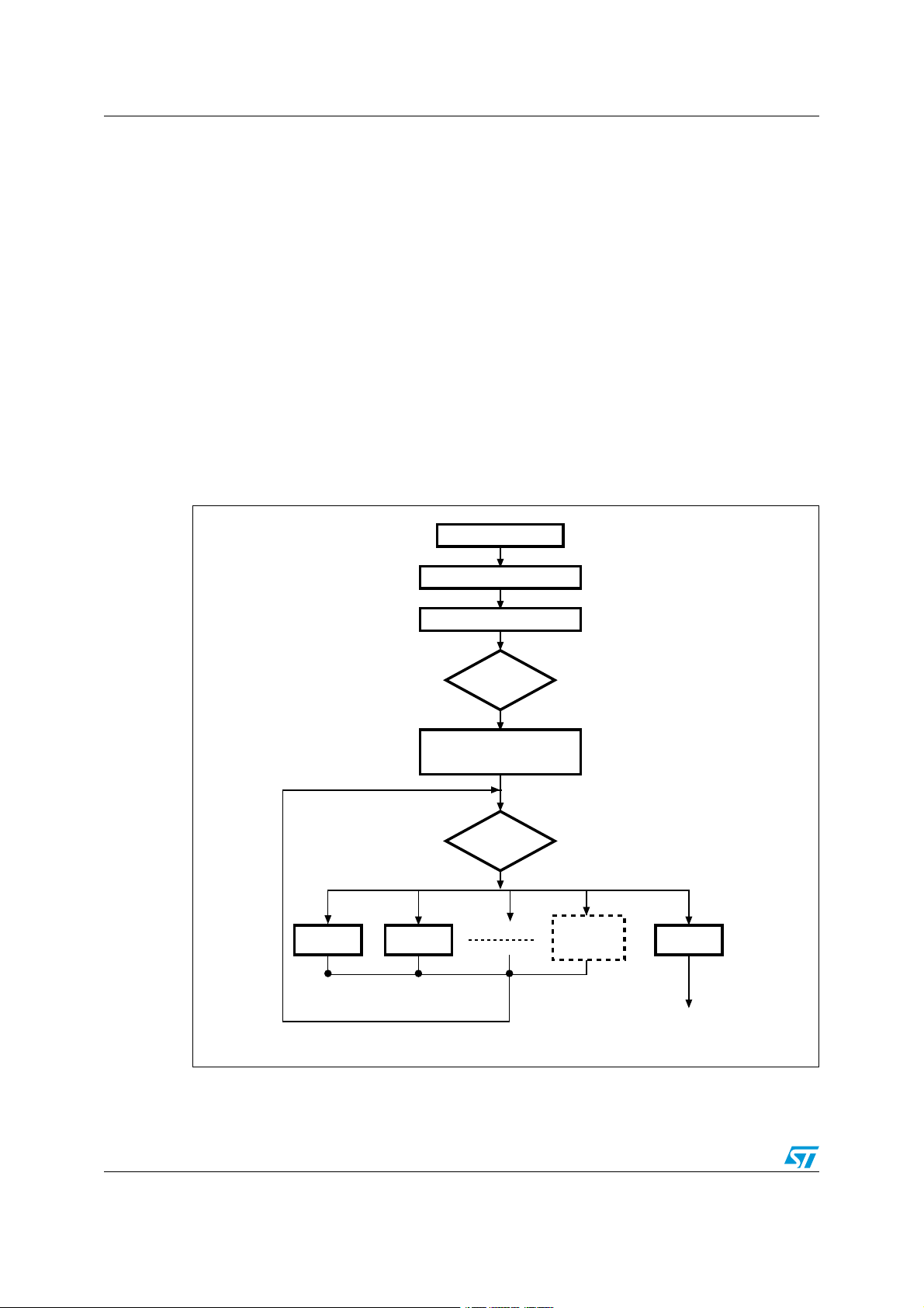
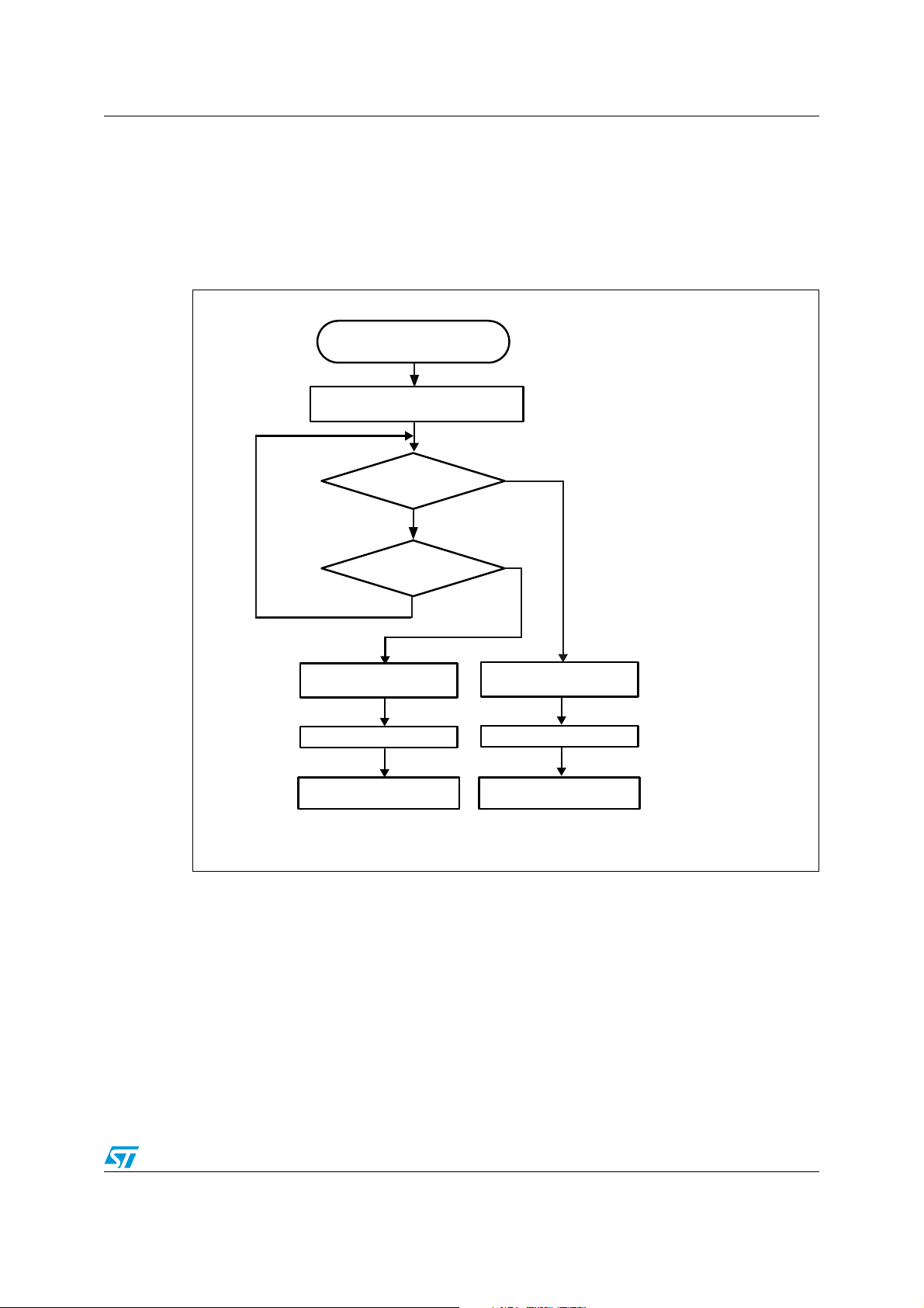
Figure 1. Bootloader for STM32F10xxx with USART1
'%4CMD
14/88 Doc ID 13801 Rev 14
OMMAND
RECEIVED
'/CMD
Page 15

AN2606 STM32F100xx, STM32F101xx, STM32F102xx, STM32F103xx, medium-density and high-
Once System memory boot mode is entered and the microcontroller has been configured as
described above, the bootloader code begins to scan the USART1_RX line pin, waiting to
receive the 0x7F data frame: one start bit, 0x7F data bits, even parity bit and one stop bit.
The duration of this data frame is measured using the Systick timer. The count value of the
timer is then used to calculate the corresponding baud rate factor with respect to the current
system clock.
Next, the code initializes the serial interface accordingly. Using this calculated baud rate, an
acknowledge byte (0x79) is returned to the host, which signals that the STM32F10xxx is
ready to receive user commands.
4.4 Bootloader version
Ta bl e 5 lists the bootloader versions of the STM32F10xxx devices.
Table 5. STM32F10xxx bootloader versions
Bootloader version number Description
V2.0 Initial bootloader version.
– Updated Go Command to initialize the main stack pointer
– Updated Go command to return NACK when jump address is in
V2.1
V2.2
the Option byte area or System memory area
– Updated Get ID command to return the device ID on two bytes
– Update the bootloader version to V2.1
– Updated Read Memory, Write Memory and Go commands to
deny access with a NACK response to the first 0x200 bytes of
RAM memory used by the bootloader
– Updated Readout Unprotect command to initialize the whole
RAM content to 0x0 before ROP disable operation
Doc ID 13801 Rev 14 15/88
Page 16

STM32F105xx and STM32F107xx device bootloader AN2606
5 STM32F105xx and STM32F107xx device bootloader
5.1 Bootloader configuration
The bootloader embedded in the STM32F105xx and STM32F107xx devices supports four
serial peripherals: USART1, USART2, CAN2, and DFU (USB). This means that four serial
peripherals are supported: USART1, USART2, CAN2 and DFU (USB).
The following table shows the hardware resources required by STM32F105xx and
STM32F107xx devices used by the bootloader in System memory boot mode.
Table 6. STM32F105xx/107xx configuration in System memory boot mode
Bootloader Feature/Peripheral State Comment
Common to
all
bootloaders
RCC
HSI enabled
HSE enabled
-
The system clock frequency is 24 MHz using the PLL.
This is used only for USART1 and USART2
bootloaders and during CAN2, USB detection for
CAN and DFU bootloaders (Once CAN or DFU
bootloader is selected, the clock source will be
derived from external crystal).
The external clock is mandatory only for DFU and
CAN bootloaders and it must provide one of the
following frequencies: 8 MHz, 14.7456 MHz or
25 MHz.
For CAN Bootloader, the PLL is used only to generate
48 MHz when 14.7456 MHz is used as HSE.
For DFU Bootloader, the PLL is used to generate a
48 MHz system clock from all supported external
clock frequencies.
The clock security system (CSS) interrupt is enabled
for the CAN and DFU bootloaders. Any failure (or
removal) of the external clock will generate system
reset.
The independent watchdog (IWDG) prescaler is
configured to its maximum value and is periodically
IWDG -
System memory -
RAM -
USART1 Enabled
USART1
bootloader
16/88 Doc ID 13801 Rev 14
USART1_RX pin Input PA10 pin: USART1 receive
USART1_TX pin Output push-pull PA9 pin: USART1 transmit
USART2_RX (PD6), CAN2_RX (PB5), OTG_FS_DM (PA11) and OTG_FS_DP (PA12) pins must be
kept at a high or low level during the detection phase.
refreshed to prevent watchdog reset (in case the
hardware IWDG option was previously enabled by the
user).
18 Kbytes starting from address 0x1FFF B000,
contain the bootloader firmware
4 Kbytes starting from address 0x2000 0000 are used
by the bootloader firmware.
Once initialized the USART1 configuration is: 8-bits,
even parity and 1 Stop bit
Page 17

AN2606 STM32F105xx and STM32F107xx device bootloader
Table 6. STM32F105xx/107xx configuration in System memory boot mode (continued)
Bootloader Feature/Peripheral State Comment
USART1 and
USART2
bootloaders
USART2
bootloader
CAN2
bootloader
DFU
bootloader
SysTick timer Enabled
USART2 Enabled
USART2_RX pin Input PD6 pin: USART2 receive (remapped pin)
USART2_TX pin Output push-pull PD5 pin: USART2 transmit (remapped pin)
USART1_RX (PA10), CAN2_RX (PB5), OTG_FS_DM (PA11) and OTG_FS_DP (PA12) pins must
be kept at a high or low level during the detection phase.
CAN2 Enabled
CAN2_RX pin Input PB5 pin: CAN2 receives (remapped pin)
CAN2_TX pin Output push-pull PB6 pin: CAN2 transmits (remapped pin)
USART1_RX (PA10), USART2_RX (PD6), OTG_FS_DM (PA11) and OTG_FS_DP (PA12) pins
must be kept at a high or low level during the detection phase.
USB OTG FS Enabled USB OTG FS configured in Forced Device mode
OTG_FS_VBUS pin
OTG_FS_DM pin PA11: USB Send-Receive data line
OTG_FS_DP pin PA12: USB Send-Receive data line
Interrupts Enabled
Input or alternate
function, automatically
controlled by the USB
OTG FS controller
Used to automatically detect the serial baud rate from
the host for USARTx bootloader.
Once initialized the USART2 configuration is: 8-bits,
even parity and 1 Stop bit. The USART2 uses its
remapped pins.
Once initialized the CAN2 configuration is: Baudrate
125 kbps, 11-bit identifier.
Note: CAN1 is clocked during the CAN bootloader
execution because in STM32F105xx and
STM32F107xx devices, CAN1 manages the
communication between CAN2 and SRAM.
PA9: Power supply voltage line
USB_OTG_FS interrupt vector is enabled and used
for USB DFU communication.
USART1_RX (PA10), USART2_RX (PD6) and CAN2_RX (PB5) pins must be kept at a high or low
level during the detection phase.
The system clock is derived from the embedded internal high-speed RC for USARTx
bootloader. This internal clock is used also for DFU and CAN bootloaders but only for the
selection phase. An external clock (8 MHz, 14.7456 MHz or 25 MHz.) is required for DFU
and CAN bootloader execution after the selection phase.
After downloading the application binary, if you choose to execute the Go command, all
peripheral registers used by the bootloader (shown in the above table) will be initialized to
their default reset values before jumping to the user application.
If the user application uses the IWDG, the IWDG prescaler value has to be adapted to meet
the requirements of the application (since the prescaler was set to its maximum value by the
bootloader).
Doc ID 13801 Rev 14 17/88
Page 18

STM32F105xx and STM32F107xx device bootloader AN2606
5.2 Bootloader hardware requirements
The hardware required to put the STM32F105xx and STM32F107xx into System memory
boot mode consists of any circuitry, switch or jumper, capable of holding the BOOT0 pin high
and the BOOT1 pin low during reset.
To connect to the STM32F105xx and STM32F107xx during System memory boot mode, the
following conditions have to be verified:
● The RX pins of the unused peripherals in this bootloader have to be kept at a known
(low or high) level, and should not be left floating during the detection phase as
described below:
– If USART1 is used to connect to the bootloader: the USART2_RX (PD6),
CAN2_RX (PB5), OTG_FS_DM (PA11) and OTG_FS_DP (PA12) pins have to be
kept at a high or low level and must not be left floating during the detection phase.
– If USART2 is used to connect to the bootloader: the USART1_RX (PA10),
CAN2_RX (PB5), OTG_FS_DM (PA11) and OTG_FS_DP (PA12) pins have to be
kept at a high or low level and must not be left floating during the detection phase.
– If CAN2 is used to connect to the bootloader: the USART1_RX (PA10),
USART2_RX (PD6), OTG_FS_DM (PA11) and OTG_FS_DP (PA12) pins have to
be kept at a high or low level and must not be left floating during the detection
phase.
– If DFU is used to connect to the bootloader: the USART1_RX (PA10),
USART2_RX (PD6) and CAN2_RX (PB5) pins have to be kept at a high or low
level and must not be left floating during the detection phase.
● Connection to the peripheral to be performed through:
– an RS232 serial interface (example, ST3232 RS232 transceiver) has to be directly
connected to the USART1_RX (PA10) and USART1_TX (PA9) pins when
USART1 is used, or to the USART2_RX (PD6) and USART2_TX (PD5) pins when
USART2 is used
– a CAN interface (CAN transceiver) has to be directly connected to the CAN2_RX
(PB5) and CAN2_TX (PB6) pins
– a certified USB cable has to be connected to the microcontroller (optionally an
ESD protection circuitry can be used)
The USART1_CK, USART1_CTS and USART1_RTS pins are not used, therefore the
application can use these pins for other peripherals or GPIOs. The same note is applicable
for USART2.
Once the USB Device is enabled, all its related pins are dedicated to USB communication
only, and cannot be used for other application purposes.
The user can control the BOOT0 and Reset pins from a PC serial applet using the RS232
serial interface which controls BOOT0 through the CTS line and Reset through the DCD
line. The user must use a full null modem cable. The necessary hardware to implement for
this control exists in the STM3210C-EVAL board. For more details about this, refer to
document: “STM3210C-EVAL board user manual”, available from the STMicroelectronics
website: http://www.st.com.
18/88 Doc ID 13801 Rev 14
Page 19

AN2606 STM32F105xx and STM32F107xx device bootloader
5.3 Bootloader selection
The STM32F105xx and STM32F107xx embedded bootloader supports four peripherals
interfaces: USART1, USART2, CAN2 and DFU (USB). Any one of these peripheral
interfaces can be used to communicate with the bootloader and download the application
code to the internal Flash.
The embedded bootloader firmware is able to auto-detect the peripheral interface to be
used. In an infinite loop, it detects any communication on the supported bootloader
interfaces.
Note: The RX pins of the peripherals not used in this bootloader must be kept at a known
(low or high) level and should not be left floating during the detection phase as
described below. Refer to Section 5.2: Bootloader hardware requirements for more
information.
To use the USART bootloader on USART1 or USART2, connect the serial cable to the
desired interface. Once the bootloader detects the data byte 0x7F on this interface, the
bootloader firmware executes the auto-baud rate sequence and then enters a loop, waiting
for any USART bootloader command.
To use the CAN2 interface, connect the CAN cable to CAN2. Once the bootloader detects a
frame on the CAN2_RX pin (PB5), the bootloader firmware enters a CAN loop and starts to
check the external clock frequency value, if the HSE is 8 MHz, 14.7456 MHz or 25 MHz
CAN bootloader firmware enters an infinite loop and waits until it receives a message,
otherwise a system reset is generated.
If a USB cable is plugged into the microcontroller’s USB interface at any time during the
bootloader firmware selection sequence, the bootloader then enters the DFU bootloader
loop waiting for any DFU bootloader command.
To use the USART or the CAN bootloader, it is mandatory that no USB cable is connected to
the USB peripheral during the selection phase. Once the USART or CAN bootloader is
selected, the user can plug a USB cable without impacting the selected bootloader
execution except commands which generate a system reset.
Once one interface is selected for the bootloader, all other interfaces are disabled.
The figure below shows the bootloader detection mechanism. More details are provided in
the sections corresponding to each peripheral bootloader.
Doc ID 13801 Rev 14 19/88
Page 20
STM32F105xx and STM32F107xx device bootloader AN2606
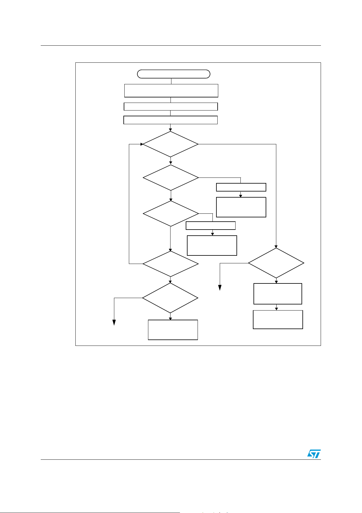
Figure 2. Bootloader selection for STM32F105xx and STM32F107xx devices
System reset
No
No
Generate system
reset
System init (clock, GPIOs, IWDG,
SysTick)
Configure CAN2
Configure USB
USB cable
detected
No
0x7F received on
USART1
No
0x7F received on
USART2
No
Frame detected on
CAN2_RX pin
Ye s
HSE = 8 MHz,
14.7456 MHz or
25 MHz
Ye s
Execute
BL_CAN_Loop for
CAN2
Ye s
Ye s
Ye s
Configure USART2
BL_USART_Loop for
Configure USART1
BL_USART_Loop for
Execute
USART2
Generate system
reset
Execute
USART1
No
HSE = 8 MHz,
14.7456 MHz or
25 MHz
Ye s
Reconfigure system
clock to 48 MHz and
USB clock to 48 MHz
Execute DFU boot-
loader using USB
interrupts
ai17514
20/88 Doc ID 13801 Rev 14
Page 21

AN2606 STM32F105xx and STM32F107xx device bootloader
5.4 Bootloader version
The table below lists the bootloader versions and the changes between all versions of the
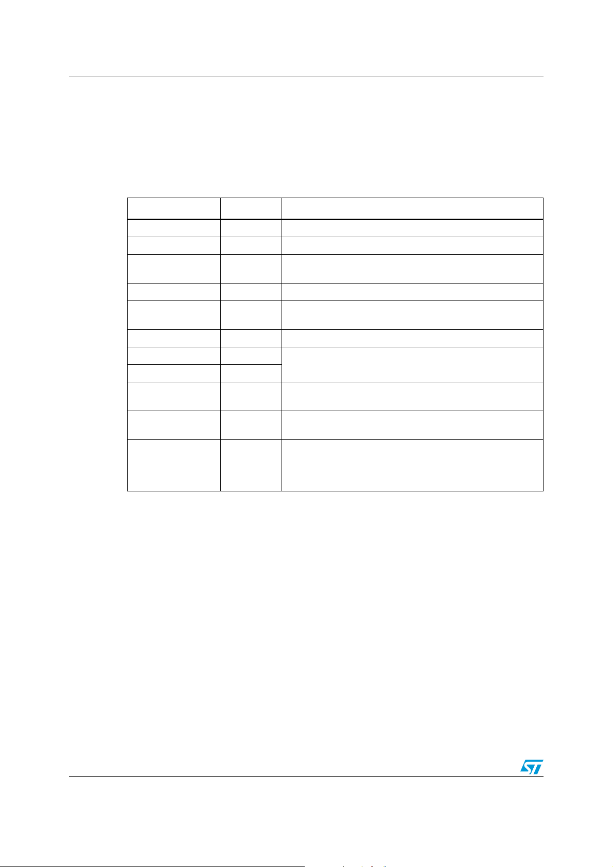
STM32F105xx and STM32F107xx devices.
Table 7. STM32F105xx and STM32F107xx bootloader versions
Bootloader version
number
V1.0 Initial bootloader version.
V2.0
– Bootloader detection mechanism updated to fix the issue when GPIOs of
unused peripherals in this bootloader are connected to low level or left
floating during the detection phase.
For more details please refer to Section 5.4.2.
– Vector table set to 0x1FFF B000 instead of 0x0000 0000
– Go command updated (for all bootloaders): USART1, USART2, CAN2,
GPIOA, GPIOB, GPIOD and SysTick peripheral registers are set to their
default reset values
– DFU bootloader: USB pending interrupt cleared before executing the Leave
DFU command
– DFU subprotocol version changed from V1.0 to V1.2
– Bootloader version updated to V2.0
Description
– Fixed PA9 excessive consumption described in Section 5.4.4.
V2.1
V2.2
– Get-Version command (defined in AN3155) corrected. It returns 0x22
instead of 0x20 in bootloader V2.0. Refer to Section 5.4.3 for more details.
– Bootloader version updated to V2.1
– Fixed DFU option bytes descriptor (set to ‘e’ instead of ‘g’ because it is
read/write and not erasable).
– Fixed DFU polling timings for Flash Read/Write/Erase operations.
– Robustness enhancements for DFU bootloader interface.
– Updated Bootloader version to V2.2.
5.4.1 How to identify STM32F105xx/107xx bootloader versions
Bootloader V1.0 is implemented on devices which date code is below 937 (refer to
STM32F105xx and STM32F107xx datasheet for where to find the date code on the device
marking). Bootloader V2.0 and V2.1 are implemented on devices with a date code higher or
equal to 937.
There are two ways to distinguish between bootloader versions:
● When using the USART bootloader, the Get-Version command defined in AN2606 and
AN3155 has been corrected in V2.1 version. It returns 0x22 instead of 0x20 as in
bootloader V2.0.
● The values of the vector table at the beginning of the bootloader code are different. The
user software (or via JTAG/SWD) reads 0x1FFFE945 at address 0x1FFFB004 for
Doc ID 13801 Rev 14 21/88
Page 22

STM32F105xx and STM32F107xx device bootloader AN2606
bootloader V2.0 0x1FFFE9A1 for bootloader V2.1, and 0x1FFFE9C1 for bootloader
V2.2.
● The DFU version is the following:
– V2.1 in Bootloader V2.1
– V2.2 in Bootloader V2.2.
It can be read through the bcdDevice field of the DFU Device Descriptor.
5.4.2 Bootloader unavailability on STM32F105xx/STM32F107xx devices with a date code below 937
Description
The bootloader cannot be used if the USART1_RX (PA10), USART2_RX (PD6, remapped),
CAN2_Rx (PB5, remapped), OTG_FS_DM (PA11), and/or OTG_FS_DP (PA12) pin(s) are
held low or left floating during the bootloader activation phase.
The bootloader cannot be connected through CAN2 (remapped), DFU (OTG FS in Device
mode), USART1 or USART2 (remapped).
On 64-pin packages, the USART2_RX signal remapped PD6 pin is not available and it is
internally grounded. In this case, the bootloader cannot be used at all.
Workaround
● For 64-pin packages
None. The bootloader cannot be used.
● For 100-pin packages
Depending on the used peripheral, the pins for the unused peripherals have to be kept
at a high level during the bootloader activation phase as described below:
– If USART1 is used to connect to the bootloader, PD6 and PB5 have to be kept at a
high level.
– If USART2 is used to connect to the bootloader, PA10, PB5, PA11 and PA12 have
to be kept at a high level.
– If CAN2 is used to connect to the bootloader, PA10, PD6, PA11 and PA12 have to
be kept at a high level.
– If DFU is used to connect to the bootloader, PA10, PB5 and PD6 have to be kept at
a high level.
Note: This limitation applies only to STM32F105xx and STM32F107xx devices with a date code
below 937. STM32F105xx and STM32F107xx devices with a date code higher or equal to
937 are not impacted. See STM32F105xx and STM32F107xx datasheet for where to find
the date code on the device marking.
5.4.3 USART bootloader Get-Version command returns 0x20 instead of 0x22
Description
In USART mode, the Get-Version command (defined in AN3155) returns 0x20 instead of
0x20.
22/88 Doc ID 13801 Rev 14
Page 23

AN2606 STM32F105xx and STM32F107xx device bootloader
This limitation is present on bootloader versions V1.0 and V2.0, while it is fixed in bootloader
version 2.1.
Workaround
None.
5.4.4 PA9 excessive power consumption when USB cable is plugged in bootloader V2.0
Description
When connecting an USB cable after booting from System-Memory mode, PA9 pin
(connected to V
push-pull and forced to 0 since the USART peripheral is not yet clocked. As a consequence,
a current higher than 25 mA is drained by PA9 I/O and may affect the I/O pad reliability.
This limitation is fixed in bootloader version 2.1 by configuring PA9 as alternate function
push-pull when a correct 0x7F is received on RX pin and the USART is clocked. Otherwise,
PA9 is configured as alternate input floating.
Workaround
None.
=5 V) is also shared with USART TX pin which is configured as alternate
BUS
Doc ID 13801 Rev 14 23/88
Page 24

STM32F101xx and STM32F103xx XL-density device bootloader AN2606
6 STM32F101xx and STM32F103xx XL-density device
bootloader
Throughout this section STM32F10xxx XL-density is used to refer to XL-density
STM32F101xx and STM32F103xx devices.
6.1 Dual bank boot feature
For STM32F101xx and STM32F103xx XL-density devices (these devices have two Flash
memory banks: Bank 1 and Bank 2), an additional boot mechanism is available which allows
booting from Bank 2 or Bank 1 (depending on the BFB2 bit status (bit 19 in the user option
bytes @ 0x1FFFF800)).
1. When the BFB2 bit is reset, and the boot pins are configured to boot from the Flash
memory (BOOT0 = 0 and BOOT1 = x) then, after reset, the device boots from the
System memory and executes the embedded bootloader code which implements the
dual bank Boot mode:
a) First, the code checks Bank 2. If it contains a valid code (see Note: below), it
jumps to application located in Bank 2 and leaves the Bootloader.
b) If the Bank 2 code is not valid, it checks Bank 1 code. If it is valid (see “note”
below), it jumps to the application located in Bank 1.
c) If both Bank 2 and Bank 1 do not contain valid code (see “note” below), the normal
Bootloader operations are executed as described in the following sections (no
jump to Flash banks is executed). Refer to Figure 3: Bootloader selection for
STM32F10xxx XL-density devices for more details.
2. When the bit BFB2 is set (default state), the dual bank boot mechanism is not
performed.
Note: The code is considered as valid when the first data (at the bank start address, which should
be the stack pointer) points to a valid address into the internal SRAM memory (stack top
address). If the first address points to any other location (out of the internal SRAM) the code
is considered not valid.
A dual bank Boot mode example (FLASH\Dual_Boot) is provided within the STM32F10x
Standard Peripheral Library available on http://www.st.com.
24/88 Doc ID 13801 Rev 14
Page 25
AN2606 STM32F101xx and STM32F103xx XL-density device bootloader
For the STM32F101xx and STM32F103xx XL-density devices, the Flash memory, system
memory or SRAM is selected as the boot space, as shown in Tab le 8 below.
Table 8. Boot pin and BFB2 bit configuration
Boot mode
BFB2
bit
selection pins
BOOT1 BOOT0
Boot mode Aliasing
X 0 User Flash memory
1
0
0 1 System memory System memory is selected as the boot space
1 1 Embedded SRAM
X 0 System memory
0 1 System memory
1 1 Embedded SRAM
User Flash memory is selected as the boot
space
Embedded SRAM is selected as the boot
space
System memory is selected as the boot space
then dual bank mechanism is executed
System memory is selected as the boot space
then dual bank mechanism is executed
Embedded SRAM is selected as the boot
space
Ta bl e 8 shows that the XL-density devices enter System memory boot mode in two cases:
1. If the BOOT pins are configured as follows: BOOT0 = 1 and BOOT1 = 0
2. Or if:
a) the BFB2 bit is reset and
b) boot pins are configured as follows: BOOT0 = 0 and BOOT1 = x
Note: When conditions a, b, and c below are fulfilled, it is equivalent to configuring boot pins for
system memory boot (BOOT0 = 1 and BOOT1 = 0). In this case normal Bootloader
operations are executed.
a) BFB2 bit is reset
b) Both banks don’t contain valid code
c) Boot pins configured as follows: BOOT0 = 0 and BOOT1 = x
When the BFB2 bit is cleared, and Bank 2 and/or Bank 1 contain valid user application
code, the Dual Bank Boot is always performed (bootloader always jumps to the user code
and never continues normal operations).
Consequently, if you have cleared the BFB2 bit (to boot from Bank 2) then, to be able to
execute the Bootloader code, you have to:
- either, set the BFB2 bit to 1
- or, program the content of address 0x0808 0000 (base address of Bank2) and 0x0800
0000 (base address of Bank1) to 0x0
Doc ID 13801 Rev 14 25/88
Page 26
STM32F101xx and STM32F103xx XL-density device bootloader AN2606
6.2 Bootloader configuration
The bootloader embedded in STM32F10xxx XL-density supports two serial interfaces:
USART1 and USART2.
The following table shows the required hardware resources of STM32F10xxx XL-density
devices used by the bootloader in System memory boot mode.
Table 9. STM32F10xxx XL-density configuration in System memory boot mode
Feature/peripheral State Comment
Clock source HSI enabled The system clock is equal to 24 MHz using the PLL
USART1_RX pin Input PA10 pin: USART1 receives
USART1_TX pin
USART2_RX pin Input PD6 pin: USART2 receives (remapped pins)
USART2_TX pin
SysTick timer Enabled Used to automatically detect the serial baud rate from the host
Output pushpull
Output pushpull
PA9 pin: USART1 transmits
PD5 pin: USART2 transmits (remapped pins)
USART1 Enabled
USART2 Enabled
RAM -
System memory -
IWDG -
Once initialized the USART1/USART2 configuration is: 8-bits,
even parity and 1 Stop bit.
2 Kbytes starting from address 0x2000 0000 are used by the
bootloader firmware
6 Kbytes starting from address 0x1FFF E000, contain the
bootloader firmware
The independent watchdog (IWDG) prescaler is configured to
its maximum value and is periodically refreshed to prevent
watchdog reset (in case the hardware IWDG option was
previously enabled by the user)
The system clock is derived from the embedded internal high-speed RC, no external quartz
is required for the bootloader code.
After downloading the application binary, if you choose to execute the Go command, all
peripheral registers used by the bootloader (shown in Tab le 9 ) are initialized to their default
reset values before jumping to the user application.
If the user application uses the IWDG, the IWDG prescaler value has to be adapted to meet
the requirements of the application (since the prescaler was set to its maximum value by the
bootloader).
26/88 Doc ID 13801 Rev 14
Page 27

AN2606 STM32F101xx and STM32F103xx XL-density device bootloader
6.3 Bootloader hardware requirements
The hardware required to put the STM32F10xx XL-density devices into System memory
boot mode consists of any circuitry, switch or jumper, capable of holding the BOOT0 pin high
and the BOOT1 pin low during reset.
Note: As explained in Section 6.1: Dual bank boot feature, the System memory boot mode can
also be executed by software when the BFB2 bit is reset, both banks start addresses are
erased, and boot pins are configured to boot from Flash memory.
To connect to the STM32F10xx XL-density devices during System memory boot mode, the
following conditions have to be verified:
● The RX pin of the peripherals unused in this bootloader have to be kept at a known (low
or high) level, and should not be left floating during the detection phase as described
below:
– If the USART1 is used to connect to the bootloader: the USART2_RX (PD6) pin
has to be kept at a high or low level and must not be left floating during the
detection phase.
– If the USART2 is used to connect to the bootloader: the USART1_RX (PA10) pin
has to be kept at a high or low level and must not be left floating during the
detection phase.
● When the BFB2 bit is cleared, and Bank 2 and/or Bank 1 contain a valid user
application code, the Dual Bank Boot is always performed (bootloader always jumps to
the user code and never continues normal operations). Consequently, if you have
cleared the BFB2 bit (to boot from Bank 2), then to be able to execute the Bootloader
code, you have to:
– either, set the BFB2 bit to 1
– or, program the content of address 0x0808 0000 (base address of Bank2) and
0x0800 0000 (base address of Bank1) to 0x0
● Connection to the peripheral to be performed through:
– an RS232 serial interface (example, ST3232 RS232 transceiver) has to be directly
connected to the USART1_RX (PA10) and USART1_TX (PA9) pins when
USART1 is used, or to the USART2_RX (PD6) and USART2_TX (PD5) pins when
USART2 is used
The USART1_CK, USART1_CTS and USART1_RTS pins are not used, therefore the
application can use these pins for other peripherals or GPIOs. This is also applicable for
USART2.
Doc ID 13801 Rev 14 27/88
Page 28

STM32F101xx and STM32F103xx XL-density device bootloader AN2606
6.4 Bootloader selection
The STM32F10xx XL-density embedded Bootloader supports two peripheral interfaces:
USART1 and USART2. Any one of these peripheral interfaces can be used to communicate
with the bootloader and download the application code to the internal Flash.
The embedded Bootloader firmware is able to auto-detect the peripheral interface to be
used. In an infinite loop, it detects any communication on the supported bootloader
interfaces.
Note: The RX pins of the peripherals not used in this bootloader must be kept at a known
(low or high) level and should not be left floating during the detection phase as
described below. Refer to Section 6.3: Bootloader hardware requirements for more
information.
To use the USART bootloader on USART1 or USART2, connect the serial cable to the
desired interface. Once the bootloader detects the data byte 0x7F on this interface, the
bootloader firmware executes the auto-baudrate sequence and then enters a loop, waiting
for any USART bootloader command.
Once one interface is selected for the bootloader, the other interface is disabled.
Figure 3 shows the bootloader detection mechanism. More details are provided in the
sections corresponding to each peripheral bootloader.
28/88 Doc ID 13801 Rev 14
Page 29

AN2606 STM32F101xx and STM32F103xx XL-density device bootloader
3YSTEM2ESET
"&"BITISRESET
"&"
)FVALUE XIS
WITHININT32!-ADDRESS
9%3
9%3
)FVALUE XIS
WITHININT32!-ADDRESS
*UMPTOUSERCODEIN
"ANK
*UMPTOUSERCODEIN
"ANK
./
./
#ONTINUENORMAL"OOTLOADER
EXECUTION
./
$ISABLEALLINTERRUPTSOURCES
3YSTEMINITCLOCK'0)/S)7$'
3YS4ICK
X&RECEIVED
ON53!24
X&RECEIVED
ON53!24
#ONFIGURE53!24
%XECUTE",?53!24?,OOP
FOR53!24
#ONFIGURE53!24
%XECUTE",?53!24?,OOP
FOR53!24
9%3
9%3
9%3
./
./
AI
Figure 3. Bootloader selection for STM32F10xxx XL-density devices
Doc ID 13801 Rev 14 29/88
Page 30

STM32F101xx and STM32F103xx XL-density device bootloader AN2606
6.5 Bootloader version
Ta bl e 1 0 lists the bootloader versions for the STM32F101xx and STM32F103xx XL-density
devices.
Table 10. XL-density bootloader versions
Bootloader version
number
V2.1 Initial bootloader version
Description
30/88 Doc ID 13801 Rev 14
Page 31

AN2606 STM32L15xx Medium-density Ultralow power device bootloader
7 STM32L15xx Medium-density Ultralow power device
bootloader
Through all this section STM32L15xxx will be used as reference to Medium-density
STM32L151xx and STM32L152xx ultralow power devices.
7.1 Bootloader configuration
The bootloader embedded in STM32L15xxx devices supports two serial interfaces:
USART1 and USART2 peripherals.
The following table shows the required hardware resources of STM32L15xx devices used
by the bootloader in System memory boot mode.
Table 11. STM32L15xxx configuration in System memory boot mode
Feature/Peripheral State Comment
Clock source HSI enabled The system clock is equal to 16 MHz
USART1_RX pin Input PA10 pin: USART1 receives
USART1_TX pin Output PA9 pin: USART1 transmits
USART2_RX pin Input PD06 pin: USART2 receives
USART2_TX pin Output PD05 pin: USART2 transmits
SysTick timer Enabled Used to automatically detect the serial baud rate from the host.
USART1 Enabled
USART2 Enabled
RAM -
System memory -
IWDG -
Power - Voltage range is set to Voltage Range 2
Once initialized the USART1 configuration is: 8-bits, even parity
and 1 Stop bit
Once initialized the USART2 configuration is: 8-bits, even parity
and 1 Stop bit
2 Kbytes starting from address 0x2000 0000 are used by the
bootloader firmware
4 Kbytes starting from address 0x1FF0 0000, contain the
bootloader firmware
The independent watchdog (IWDG) prescaler is configured to its
maximum value and is periodically refreshed to prevent
watchdog reset (in case the hardware IWDG option was
previously enabled by the user)
The system clock is derived from the embedded internal high-speed RC, no external quartz
is required for the bootloader code
After downloading the application binary, if you choose to execute the Go command, all
peripheral registers used by the bootloader (shown in the above table) are initialized to their
default reset values before jumping to the user application. If the user application uses the
IWDG, the IWDG prescaler value has to be adapted to meet the requirements of the
application (since the prescaler was set to its maximum value by the bootloader).
Doc ID 13801 Rev 14 31/88
Page 32

STM32L15xx Medium-density Ultralow power device bootloader AN2606
7.2 Bootloader hardware requirements
The hardware required to put the STM32L15xx devices into System memory boot mode
consists of any circuitry, switch or jumper, capable of holding the BOOT0 pin high and the
BOOT1 pin low during reset.
To connect to the STM32L15xx devices during System memory boot mode, the following
conditions have to be verified:
● The RX pins of the peripherals unused in this bootloader have to be kept at a known
(low or high) level, and should not be left floating during the detection phase as
described below:
– If USART1 is used to connect to the bootloader: the USART2_RX (PD6) pin has to
be kept at a high or low level and must not be left floating during the detection
phase.
– If USART2 is used to connect to the bootloader: the USART1_RX (PA10) pin has
to be kept at a high or low level and must not be left floating during the detection
phase.
● The peripheral to be used has to be connected through an RS232 serial interface
(example, ST3232 RS232 transceiver) which must be:
– Directly connected to the USART1_RX (PA10) and USART1_TX (PA9) pins when
USART1 is used
– Directly connected to the USART2_RX (PD6) and USART2_TX (PD5) pins when
USART2 is used
The USART1_CK, USART1_CTS and USART1_RTS pins are not used, therefore the
application can use these pins for other peripherals or GPIOs. The same note is applicable
for USART2.
The user can control the BOOT0 and Reset pins from a PC serial applet using the RS232
serial interface which controls BOOT0 through the CTS line and Reset through the DCD
line. The user must use a full null modem cable. The necessary hardware to implement for
this control exists in the STM32L152-EVAL board. For more details about this, refer to the
“STM32L152-EVAL board user manual” (UM1009), available from the STMicroelectronics
website: http://www.st.com.
7.3 Bootloader selection
The STM32L15xx devices embedded bootloader supports two peripherals interfaces:
USART1 and USART2. Any one of these peripheral interfaces can be used to communicate
with the bootloader and download the application code to the internal Flash.
The embedded bootloader firmware is able to auto-detect the peripheral interface to be
used. In an infinite loop, it detects any communication on the supported bootloader
interfaces.
Note: The RX pins of the peripherals not used in this bootloader must be kept at a known
(low or high) level and should not be left floating during the detection phase as
described below. Refer to Section 7.2: Bootloader hardware requirements for more
information.
To use the USART bootloader on USART1 or USART2, connect the serial cable to the
desired interface. Once the bootloader detects the data byte 0x7F on this interface, the
32/88 Doc ID 13801 Rev 14
Page 33
AN2606 STM32L15xx Medium-density Ultralow power device bootloader
System reset
0x7F received
on USART1
0x7F received
on USART2
Configure USART1
Execute BL_USART_Loop
for USART1
Configure USART2
Execute BL_USART_Loop
for USART2
YES
NO
-36
System init (clock, GPIOs, IWDG,
SysTick
NO
Disable all interrupt
sources
Disable all interrupt
sources
YES
bootloader firmware executes the autobaudrate sequence and then enters a loop, waiting
for any USART bootloader command.
Once one interface is selected for the bootloader, the other interface is disabled.
The figure below shows the bootloader detection mechanism. More details are provided in
the sections corresponding to each peripheral bootloader.
Figure 4. Bootloader selection for STM32L15xxx devices
Doc ID 13801 Rev 14 33/88
Page 34

STM32L15xx Medium-density Ultralow power device bootloader AN2606
7.4 Important considerations
The bootloader of the Medium-density ultralow power devices has some specific features
that should be taken into consideration, as described below:
● In addition to standard memories (internal Flash, internal SRAM, option bytes and
System memory), the STM32L15xxx device bootloader firmware supports Data
Memory (4 Kbytes from 0x08080000 to 0x08080FFF). Refer to the PM0062
Programming manual for more information.
● Flash memory write operations are performed through a program memory half page
write operation. The bootloader firmware manages half page write operations at nonaligned addresses. Consequently, all write operations must only be Word-aligned (the
address should be a multiple of 4). The number of data to be written must also be a
multiple of 4 (non-aligned half page write addresses are accepted). Be aware of the
duration needed for a write operation by referring to the product datasheet.
● Data memory can be read and written but cannot be erased using the Erase
Command. When writing in a Data memory location, the bootloader firmware manages
the erase operation of this location before any write. A write to Data memory must be
Word-aligned (address to be written should be a multiple of 4) and the number of data
must also be a multiple of 4. To erase a Data memory location, you can write zeros at
this location.
● Option byte
Address is 0x1FF80000. They allow three levels of protection:
– Level 0
–Level 1
–Level 2
Refer to PM0062 programming manual for more details about protection levels.
● Read protect command corresponds to the Level 1 protection.
● Read unprotect command corresponds to the Level 0 protection.
● Mass erase command is not supported by STM32L15xxx device Bootloader firmware.
To perform a mass erase operation, two options are available:
– Erase all sectors one by one using the Erase command
– Set protection level to Level 1. Then, set it to Level 0 (using the Read protect
command and then the Read Unprotect command). This operation results in a
mass erase of the internal Flash memory (refer to Programming Manual PM0062
for more details).
34/88 Doc ID 13801 Rev 14
Page 35

AN2606 STM32L15xx Medium-density Ultralow power device bootloader
7.5 Bootloader version
The following table lists the STM32L15xxx bootloader versions.
Table 12. STM32L15xxx bootloader versions
Bootloader
version
number
V2.0 Initial bootloader version.
1. If the “number of data - 1” (N-1) to be read/written is not equal to a valid command code (0x00, 0x01, 0x02,
0x11, 0x21, 0x31, 0x43, 0x44, 0x63, 0x73, 0x82 or 0x92), then the limitation is not perceived from the host
since the command is NACKed anyway (as an unsupported new command).
Description Known limitations
When a Read Memory command or Write Memory
command is issued with an unsupported memory
address and a correct address checksum (ie. address
0x6000 0000), the command is aborted by the bootloader
device, but the NACK (0x1F) is not sent to the host. As a
result, the next 2 bytes (which are the number of bytes to
be read/written and its checksum) are considered as a
new command and its checksum.
(1)
Doc ID 13801 Rev 14 35/88
Page 36

STM32L15xx and STM32L16xx High-density ultralow power device bootloader AN2606
8 STM32L15xx and STM32L16xx High-density ultralow
power device bootloader
Throughout this section, STM32L1xx High-density is used to refer to STM32L15xx and
STM32L16xx High-density ultralow power devices.
8.1 Dual bank boot feature
The STM32L1xx High-density devices have two Flash memory banks: Bank 1 and Bank 2.
They feature an additional boot mechanism which allows booting from Bank 2 or Bank 1
depending on BFB2 bit status (bit 7 in the user option bytes located at 0x1FF8 0004).
● When the BFB2 bit is reset and the boot pins are configured to boot from Flash
memory (BOOT0 = 0 and BOOT1 = x), after reset the device boots from the System
memory and executes the embedded bootloader code which implements the dual bank
Boot mode:
a) The code first checks Bank 2. If it contains a valid code (see note below), it jumps
to the application code located in Bank 2 and leaves the Bootloader.
b) If the Bank 2 code is not valid, it checks Bank 1 code. If it is valid (see note below),
it jumps to the application located in Bank 1.
c) If both Bank 2 and Bank 1 do not contain valid code (see note below), the normal
Bootloader operations are executed as described in the following sections and no
jump to Flash banks is performed. Refer to Figure 5: Bootloader selection for
STM32L1xx High-density devices for more details.
3. When BFB2 bit is set (default state), the dual bank boot mechanism is not performed.
Note: The code is considered as valid when the first data (at the bank start address, which should
be the stack pointer) points to a valid address into the internal SRAM memory (stack top
address). If the first address points to any other location (out of the internal SRAM) the code
is considered not valid.
A dual bank Boot mode example (FLASH\Dual_Boot) is provided within the STM32L1xx
Standard Peripheral Library available from http://www.st.Com.
For the STM32L1xx High-density devices, the Flash memory, system memory or SRAM is
selected as the boot space, as shown in Ta bl e 13 below.
36/88 Doc ID 13801 Rev 14
Page 37

AN2606 STM32L15xx and STM32L16xx High-density ultralow power device bootloader
Table 13. Boot pin and BFB2 bit configuration
Boot mode
BFB2
bit
selection pins
Protection
level2
Bank2
Valid
Bank1
Val id
BOOT1 BOOT0
X0 X XX
0 1 No X X System memory
1
01 YesXX
1 1 No X X Embedded SRAM
11 YesXX
Yes X System memory
X
No Yes System memory
X0
No No No System memory
Boot mode Aliasing
User Flash
memory
User Flash memory Bank1 is
selected as the boot space
System memory is selected as the
boot space
User Flash
memory
User Flash memory Bank1 is
selected as the boot space
Embedded SRAM is selected as the
boot space
User Flash
memory
User Flash memory Bank1 is
selected as the boot space
User Flash memory Bank2 is
selected as the boot space
User Flash memory Bank1 is
selected as the boot space
System memory is selected as the
boot space
Yes No No System memory CPU blocked (halted)
0
0 1 No X X System memory
1 1 No X X Embedded SRAM
Yes X System memory
X1 Yes
No Yes System memory
System memory is selected as the
boot space
Embedded SRAM is selected as the
boot space
User Flash memory Bank2 is
selected as the boot space
User Flash memory Bank1 is
selected as the boot space
No No System memory CPU blocked (halted)
Ta bl e 1 3 shows that the STM32L1xx High-density devices enter System memory boot mode
in two cases:
● If the BOOT pins are configured as follows:
BOOT0 = 1 and BOOT1 = 0
● If the BFB2 bit is reset and protection Level2 is enabled
● If the BFB2 bit is reset and boot pins are configured as follows:
BOOT0 = 0 and BOOT1 = x
Doc ID 13801 Rev 14 37/88
Page 38

STM32L15xx and STM32L16xx High-density ultralow power device bootloader AN2606
Note: When the conditions a, b, and c described below are fulfilled, it is equivalent to configuring
boot pins for system memory boot (BOOT0 = 1 and BOOT1 = 0). In this case normal
Bootloader operations are executed.
a) BFB2 bit is reset
b) Both banks don’t contain valid code
c) Boot pins configured as follows: BOOT0 = 0 and BOOT1 = x
When the BFB2 bit is cleared, and Bank 2 and/or Bank 1 contain valid user application
code, the Dual Bank Boot is always performed (bootloader always jumps to the user code
and never continues normal operations).
Consequently, if you have cleared the BFB2 bit (to boot from Bank 2) then, to be able to
execute the Bootloader code, you have to:
– either, set the BFB2 bit to 1
– or, program the content of address 0x0803 0000 (base address of Bank2) and
0x0800 0000 (base address of Bank1) to 0x0.
8.2 Bootloader configuration
The bootloader embedded in STM32L1xx High-density devices supports three serial
interfaces: USART1, USART2 and DFU (USB)
The following table shows the required hardware resources of STM32L1xx High-density
devices used by the bootloader in System memory boot mode.
38/88 Doc ID 13801 Rev 14
Page 39

AN2606 STM32L15xx and STM32L16xx High-density ultralow power device bootloader
Table 14. STM32L1xx High-density configuration in System memory boot mode
Bootloader Feature/Peripheral State Comment
The system clock frequency is 16 MHz
using the HSI. This is used only for
USART1 and USART2 bootloaders and
HSI enabled
during USB detection for DFU bootloader
(once the DFU bootloader is selected, the
clock source will be derived from the
external crystal).
The external clock is mandatory only for
RCC
HSE enabled
DFU bootloader and it must be in the
following range: [24, 16, 12, 8, 6, 4, 3, 2]
MHz.
The PLL is used to generate the USB
48 MHz clock and the 32 MHz clock for the
system clock.
The clock security system (CSS) interrupt is
Common to all
bootloaders
-
enabled for the DFU bootloader. Any failure
(or removal) of the external clock generates
system reset.
The independent watchdog (IWDG)
prescaler is configured to its maximum
IWDG -
value and is periodically refreshed to
prevent watchdog reset (in case the
hardware IWDG option was previously
enabled by the user).
Power Voltage range is set to Voltage Range 2
USART1 bootloader
USART1 and
USART2 bootloaders
8 Kbytes starting from address
System memory -
0x1FF0 0000. This area contains the
bootloader firmware
4 Kbytes starting from address
RAM -
0x2000 0000 are used by the bootloader
firmware.
USART1 Enabled
Once initialized the USART1 configuration
is: 8-bits, even parity and 1 Stop bit
USART1_RX pin Input PA10 pin: USART1 in reception mode.
USART1_TX pin Output PA9 pin: USART1 in transmission mode.
USART2_RX (PD6), USB_DM (PA11) and USB_DP (PA12) pins must be kept at a high or
low level during the detection phase.
SysTick timer Enabled
Used to automatically detect the serial baud
rate from the host for USARTx bootloader.
Doc ID 13801 Rev 14 39/88
Page 40

STM32L15xx and STM32L16xx High-density ultralow power device bootloader AN2606
Table 14. STM32L1xx High-density configuration in System memory boot mode (continued)
Bootloader Feature/Peripheral State Comment
Once initialized the USART2 configuration
USART2 bootloader
USART2 Enabled
USART2_RX pin Input PD6 pin: USART2 in reception mode.
USART2_TX pin Output PD5 pin: USART2 in transmission mode.
USART1_RX (PA10), USB_DM (PA11) and USB_DP (PA12) pins must be kept at a high or
low level during the detection phase.
is: 8-bits, even parity and 1 Stop bit. The
USART2 uses its remapped pins.
DFU bootloader
USB_DM pin Input or alternate
function,
USB_DP pin PA12: USB Send-Receive data line
Interrupts Enabled
USART1_RX (PA10) and USART2_RX (PD6) pins must be kept at a high or low level
during the detection phase.
automatically
controlled by the USB
PA11: USB Send-Receive data line
USB Low Priority interrupt vector is enabled
and used for USB DFU communication.
Note: For DFU interface, the external clock source (HSE) is required for USB operations.
The detection of the HSE value is done by the Bootloader firmware and is based on
the internal oscillator clock (HSI, MSI). Thus, when due to temperature or other
conditions, the internal oscillator precision is altered above the tolerance band (1%
around theoretical value), the Bootloader might calculate a wrong HSE frequency
value. In this case, the Bootloader DFU interface might dysfunction or might not work
at all.
The system clock is derived from the embedded internal high-speed RC for USARTx
bootloader. This internal clock is used also for DFU bootloader but only for the selection
phase. An external clock in the range of [24, 16, 12, 8, 6, 4, 3, 2] MHz is required for DFU
bootloader execution after the selection phase.
After downloading the application binary, if you choose to execute the Go command, all
peripheral registers used by the bootloader (shown in the above table) are initialized to their
default reset values before jumping to the user application.
If the user application uses the IWDG, the IWDG prescaler value has to be adapted to meet
the requirements of the application (since the prescaler was set to its maximum value by the
bootloader).
40/88 Doc ID 13801 Rev 14
Page 41

AN2606 STM32L15xx and STM32L16xx High-density ultralow power device bootloader
8.3 Bootloader hardware requirements
The hardware required to put the STM32L1xx High-density devices into System memory
boot mode consists of any circuitry, switch or jumper, capable of holding the BOOT0 pin high
and the BOOT1 pin low during reset.
Note: As explained in Section 8.1: Dual bank boot feature, the System memory boot mode can
also be executed by software when the BFB2 bit is reset, both banks start addresses are
erased, and boot pins are configured to boot from Flash memory.
To connect to the STM32L1xx High-density devices during System memory boot mode, the
following conditions have to be verified:
● The RX pin of the peripherals that are not used in this bootloader have to be kept at a
known (low or high) level, and should not be left floating during the detection phase as
described below:
– If USART1 is used to connect to the bootloader: the USART2_RX (PD6),
USB_DM (PA11) and USB_DP (PA12) pins have to be kept at a high or low level
and must not be left floating during the detection phase.
– If USART2 is used to connect to the bootloader: the USART1_RX (PA10),
USB_DM (PA11) and USB_DP (PA12) pins have to be kept at a high or low level
and must not be left floating during the detection phase.
– If DFU (USB) is used to connect to the bootloader: the USART1_RX (PA10) and
USART2_RX (PD6) pins have to be kept at a high or low level and must not be left
floating during the detection phase.
● When the BFB2 bit is cleared, and Bank 2 and/or Bank 1 contain a valid user
application code, the Dual Bank Boot is always performed (bootloader always jumps to
the user code and never continues normal operations). Consequently, if you have
cleared the BFB2 bit (to boot from Bank 2), then to be able to execute the Bootloader
code, you have to:
– either, set the BFB2 bit to 1
– or, program the content of address 0x0803 0000 (base address of Bank2) and
0x0800 0000 (base address of Bank1) to 0x0
● Connection to the peripheral to be performed through:
– an RS232 serial interface (example, ST3232 RS232 transceiver) has to be directly
connected to the USART1_RX (PA10) and USART1_TX (PA9) pins when
USART1 is used, or to the USART2_RX (PD6) and USART2_TX (PD5) pins when
USART2 is used
– A certified USB cable has to be connected to the microcontroller (optionally an
ESD protection circuitry can be used).
The USART1_CK, USART1_CTS and USART1_RTS pins are not used. as a result, the
application can use these pins for other peripherals or GPIOs. This is also applicable for
USART2.
Doc ID 13801 Rev 14 41/88
Page 42

STM32L15xx and STM32L16xx High-density ultralow power device bootloader AN2606
8.4 Bootloader selection
STM32L1xx High-density embedded Bootloader supports three serial interfaces: USART1,
USART2 and DFU (USB). Any one of these peripheral interfaces can be used to
communicate with the bootloader and download the application code to the internal Flash.
The embedded Bootloader firmware is able to auto-detect the peripheral interface to be
used. In an infinite loop, it detects any communication on the supported bootloader
interfaces.
Note: The RX pins of the peripherals not used in this bootloader must be kept at a known
(low or high) level and should not be left floating during the detection phase as
described below. Refer to Section 8.3: Bootloader hardware requirements for more
information.
To use the USART bootloader on USART1 or USART2, connect the serial cable to the
desired interface. Once the bootloader detects the data byte 0x7F on this interface, the
bootloader firmware executes the auto-baudrate sequence and then enters a loop, waiting
for any USART bootloader command.
If a USB cable is plugged into the microcontroller into USB interface at any time during the
bootloader firmware selection sequence, the bootloader enters DFU bootloader loop waiting
for any DFU bootloader command.
To use the USART bootloader, it is mandatory that no USB Host is connected to the USB
peripheral during the selection phase. Once the USART bootloader is selected, the user can
plug a USB cable without impacting the selected bootloader execution except for the
commands which generate a system reset.
Once an interface is selected for the bootloader, the other interface is disabled.
Figure 5: Bootloader selection for STM32L1xx High-density devices shows the bootloader
detection mechanism. More details are provided in the sections corresponding to each
peripheral bootloader.
42/88 Doc ID 13801 Rev 14
Page 43

43/88 Doc ID 13801 Rev 14
3YSTEM2ESET
*UMPTOUSERCODE
IN"ANK
-36
0ROTECTION,EVEL
ENABLED
9%3
)FVALUE X
ISWITHININT32!-
ADDRESS
9%3
./
"&"BITRESET
"&"
9%3
)FVALUE X
ISWITHININT32!-
ADDRESS
9%3
./
*UMPTOUSERCODE
IN"ANK
)FVALUE X
ISWITHININT32!-
ADDRESS
9%3
./
./
#ONTINUENORMAL
BOOTLOADEREXECUTION
3YSTEMINITCLOCK'0)/S)7$'
3YS4ICK
X&RECEIVED
ON53!24
9%3
./
X&RECEIVED
ON53!24
$ISABLEALLINTERRUPT
SOURCES
#ONFIGURE53!24
%XECUTE",?53!24?,OOP
FOR53!24
#ONFIGURE53!24
%XECUTE",?53!24?,OOP
FOR53!24
$ISABLEALLINTERRUPT
SOURCES
9%3
9%3
./
53"ACTIVITYDETECTED
(3%DETECTED
2E#ONFIGURE$&5
53"
&3$EVICE
%XECUTE",?$&5?,OOP
./
9%3
./
'ENERATE
3YSTEM2ESET
./
*UMPTOUSERCODE
IN"ANK
*UMPTOUSERCODE
IN"ANK
)FVALUE X
ISWITHININT32!-
ADDRESS
9%3
./
#05BLOCKEDHALTED
Figure 5. Bootloader selection for STM32L1xx High-density devices
STM32L15xx and STM32L16xx High-density ultralow power device bootloader AN2606
Page 44

STM32L15xx and STM32L16xx High-density ultralow power device bootloader AN2606
8.5 Important considerations
The bootloader of the STM32L1xx High-density devices has some specific features that
should be taken into consideration, as described below:
● In addition to standard memories (internal Flash, internal SRAM, option bytes and
System memory), the STM32L1xx High-density devices bootloader firmware supports
Data Memory (12 Kbytes from 0x08080000 to 0x08082FFF). Refer to the PM0062
Programming manual for more information.
● Flash memory write operations are performed through a program memory half page
write operation. The bootloader firmware manages half page write operations at nonaligned addresses. Consequently, all write operations must only be Word-aligned (the
address should be a multiple of 4). The number of data to be written must also be a
multiple of 4 (non-aligned half page write addresses are accepted). Be aware of the
duration needed for a write operation by referring to the product datasheet.
● Data memory can be read and written but cannot be erased using the Erase
Command. When writing in a Data memory location, the bootloader firmware manages
the erase operation of this location before any write. A write to Data memory must be
Word-aligned (address to be written should be a multiple of 4) and the number of data
must also be a multiple of 4. To erase a Data memory location, you can write zeros at
this location.
● Option byte
Address is 0x1FF80000. They allow three levels of protection:
– Level 0
–Level 1
–Level 2
Refer to PM0062 programming manual for more details about protection levels.
● Read protect command corresponds to the Level 1 protection.
● Read unprotect command corresponds to the Level 0 protection.
● Mass erase command is not supported by STM32L1xx High-density devices
Bootloader firmware. To perform a mass erase operation, two options are available:
– Erase all sectors one by one using the Erase command
– Set protection level to Level 1. Then, set it to Level 0 (using the Read protect
command and then the Read Unprotect command). This operation results in a
mass erase of the internal Flash memory (refer to Programming Manual PM0062
for more details).
44/88 Doc ID 13801 Rev 14
Page 45

AN2606 STM32L15xx and STM32L16xx High-density ultralow power device bootloader
8.6 Bootloader version
Ta bl e 1 5 lists the bootloader versions for the STM32L1xx High-density devices.
Table 15. STM32L1xx High-density bootloader versions
Bootloader version number Description Known limitations
– In the Bootloader code the
PA13 (JTMS/SWDIO) I/O
output speed is configured to
400 KHz, as consequence
some debugger can not
connect to the device in Serial
Wire mode when the
Bootloader is running.
V4.1 Initial bootloader version
V4.2
V4.5
Fix V4.1 limitations (available on
Rev.Z devices only.)
Fix V4.2 limitations.
DFU interface robustness
enhancements (available on
Rev.Y devices only).
– When the DFU Bootloader is
selected, the RTC is reset and
thus all RTC information
(calendar, alarm, ...) will be
lost including backup
registers. Note: When the
USART bootloader is selected
there is no change on the
RTC configuration (including
backup registers).
– Stack overflow by 8 bytes
when jumping to
Bank1/Bank2 if BFB2=0 or
when Read Protection level is
set to 2.
Workaround: the user code
should force in the startup file
the top of stack address
before to jump to the main
program. This can be done in
the “Reset_Handler” routine.
– When the Stack of the user
code is placed outside the
SRAM (ie. @ 0x2000C000)
the Bootloader cannot jump to
that user code which is
considered invalid. This might
happen when using compilers
which place the stack at a
non-physical address at the
top of the SRAM (ie. @
0x2000C000).
Workaround: place manually
the stack at a physical
address.
None
Doc ID 13801 Rev 14 45/88
Page 46

STM32F205/215xx, and STM32F207/217xx bootloader AN2606
9 STM32F205/215xx, and STM32F207/217xx bootloader
Through all this section STM32F2xx will be used as reference to STM32F205xx,
STM32F207xx, STM32F215xx and STM32F217xx devices.
Two bootloader versions are available on STM32F2xx devices:
● V2.0 supporting USART1 and USART3
This version is embedded in STM32F2xx devices revision B.
● V3.2 supporting USART1, USART3, CAN2 and DFU (USB FS Device)
This version is embedded in STM32F2xx devices revision Y.
9.1 Bootloader V2.x
9.1.1 Bootloader configuration
The bootloader V2.x embedded in STM32F2xx devices support two serial interfaces:
USART1 and USART3 peripherals.
The following table shows the required hardware resources of STM32 devices used by the
bootloader V2.x in System memory boot mode.
Table 16. STM32F2xx configuration in System memory boot mode
Feature/Peripheral State Comment
Clock source
USART1_RX pin Input PA10 pin: USART1 receives
USART1_TX pin Output PA9 pin: USART1 transmits
USART3_RX pin Input PC11 pin: USART3 receives
USART3_TX pin Output PC10pin: USART3 transmits
USART3_RX pin Input PB11 pin: USART3 receives
USART3_TX pin Output PB10pin: USART3 transmits
SysTick timer Enabled Used to automatically detect the serial baud rate from the host.
USART1 Enabled
USART3 Enabled
RAM - 8 Kbytes starting from address 0x2000 0000
System memory -
HSI
enabled
The system clock is equal to 24 MHz
Once initialized the USART1 configuration is: 8-bits, even parity
and 1 Stop bit
Once initialized the USART3 configuration is: 8-bits, even parity
and 1 Stop bit
30688 bytes starting from address 0x1FFF 0000 contain the
bootloader firmware
46/88 Doc ID 13801 Rev 14
Page 47

AN2606 STM32F205/215xx, and STM32F207/217xx bootloader
Table 16. STM32F2xx configuration in System memory boot mode (continued)
Feature/Peripheral State Comment
The independent watchdog (IWDG) prescaler is configured to its
IWDG -
Power -
maximum value and is periodically refreshed to prevent
watchdog reset (in case the hardware IWDG option was
previously enabled by the user)
Voltage range is set to Voltage Range: [1.62V, 2.1V] (voltage
range can be configured in run time using bootloader
commands. Note that in this range internal Flash write
operations are allowed only in byte format (Half-Word, Word and
Double-Word operations are not allowed).
The system clock is derived from the embedded internal high-speed RC. No external quartz
is required for the bootloader code.
After downloading the application binary, if you choose to execute the Go command, the
peripheral registers used by the bootloader (shown in the above table) are not initialized to
their default reset values before jumping to the user application. They should be
reconfigured in the user application if they are used. So, if the IWDG is being used in the
application, the IWDG prescaler value has to be adapted to meet the requirements of the
application (since the prescaler was set to its maximum value by the bootloader).
9.1.2 Bootloader hardware requirements
The hardware required to put the STM32F2xx into System memory boot mode consists of
any circuitry, switch or jumper, capable of holding the BOOT0 pin high and the BOOT1 pin
low during reset.
To connect to the STM32F2xx during System memory boot mode, the following conditions
have to be verified:
● The RX pins of the peripherals unused in this bootloader have to be kept at a known
(low or high) level, and should not be left floating during the detection phase as
described below:
– If USART1 is used to connect to the bootloader: the USART3_RX (PC11 and
PB11) pins have to be kept at a high or low level and must not be left floating
during the detection phase.
– If USART3 (on PB10/PB11) is used to connect to the bootloader: the USART1_RX
(PA10) and the other USART3_RX pin (PC11) have to be kept at a high or low
level and must not be left floating during the detection phase.
– If USART3 (on PC10/PC11) is used to connect to the bootloader: the
USART1_RX (PA10) and the other USART3_RX pin (PB11) have to be kept at a
high or low level and must not be left floating during the detection phase.
● Connection to the peripheral to be performed through:
– An RS232 serial interface (example, ST3232 RS232 transceiver) has to be directly
connected to the USART1_RX (PA10) and USART1_TX (PA9) pins when
USART1 is used, or to the USART3_RX (PB11 or PC11) and USART3_TX (PB10
or PC10) pins or when USART3 is used.
The USART1_CK, USART1_CTS and USART1_RTS pins are not used, therefore the
application can use these pins for other peripherals or GPIOs. The same note is applicable
for USART3.
Doc ID 13801 Rev 14 47/88
Page 48

STM32F205/215xx, and STM32F207/217xx bootloader AN2606
The user can control the BOOT0 and Reset pins from a PC serial applet using the RS232
serial interface which controls BOOT0 through the CTS line and Reset through the DCD
line. The user must use a full null modem cable. The necessary hardware to implement for
this control exists in the STM322xG-EVAL board. For more details, refer to the STM322xGEVAL board user manual, available from the STMicroelectronics website: http://www.st.com.
9.1.3 Bootloader selection
The STM32F2xx embedded bootloader V2.x supports two peripheral interfaces: USART1
and USART3 (on PB10/PB11 and PC10/PC11). Any one of these peripheral interfaces can
be used to communicate with the bootloader and download the application code to the
internal Flash memory.
The embedded bootloader firmware is able to auto-detect the peripheral interface to be
used. In an infinite loop, it detects any communication on the supported bootloader
interfaces.
Note: The RX pins of the peripherals not used in this bootloader must be kept at a known
(low or high) level and should not be left floating during the detection phase as
described below. Refer to Section 9.1.2: Bootloader hardware requirements for more
information.
To use the USART bootloader on USART1 or USART3, connect the serial cable to the
desired interface. Once the bootloader detects the data byte 0x7F on this interface, the
bootloader firmware executes the autobaudrate detection sequence and enters a loop,
waiting for any USART bootloader command.
Once an interface is selected for the bootloader, the other interfaces are disabled.
Figure 6 shows the bootloader detection mechanism. More details are provided in the
sections corresponding to each peripheral bootloader.
48/88 Doc ID 13801 Rev 14
Page 49
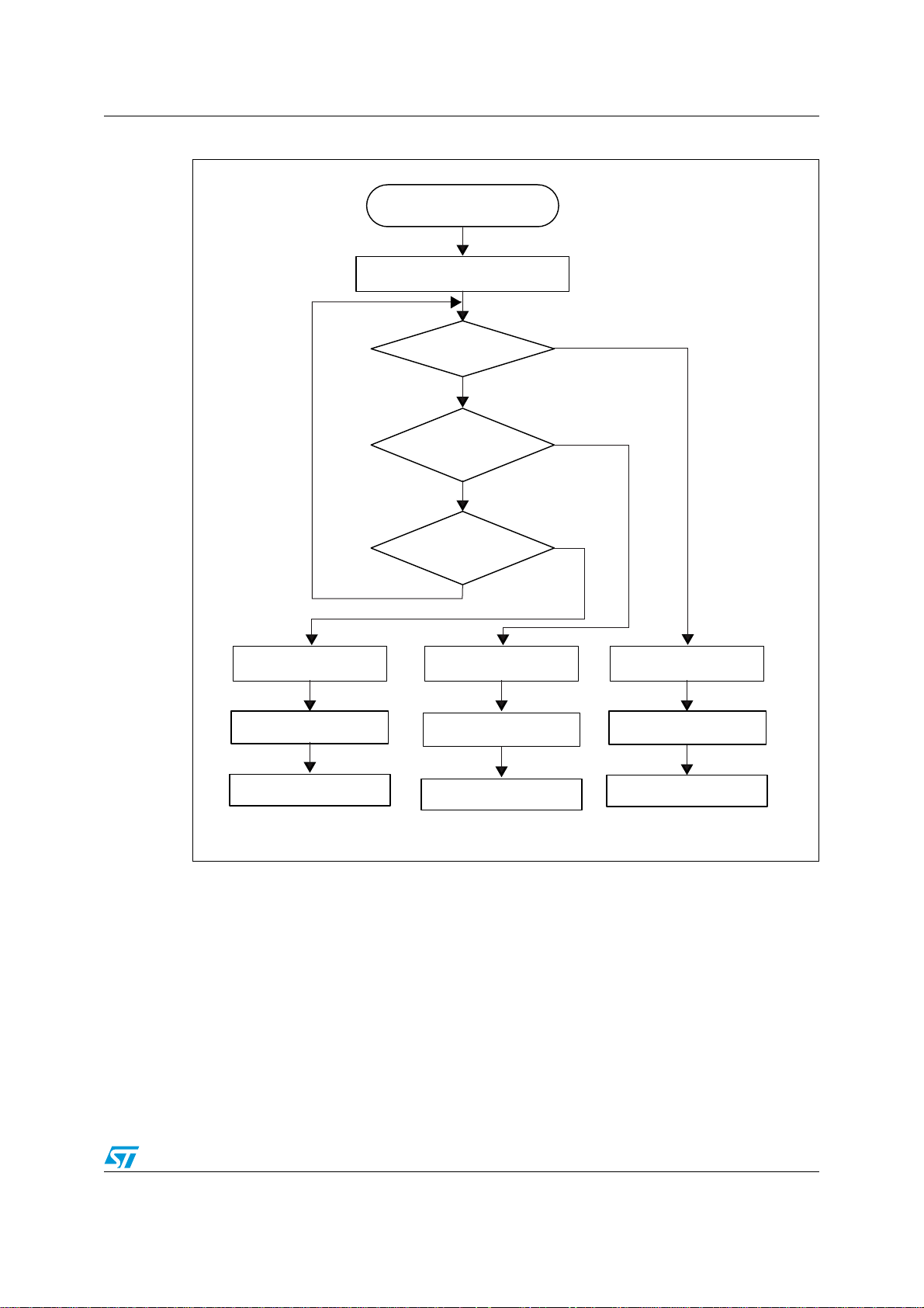
AN2606 STM32F205/215xx, and STM32F207/217xx bootloader
System Reset
System init (clock, GPIOs, IWDG,
SysTick)
0x7F received
on USART1
YES
NO
0x7F received
on USART3
(PB10/PB11)
YES
NO
0x7F received
on USART3
(PC10/PC11)
NO
Disable all interrupt
sources
Configure USART3 on
PC10/PC11 pins
Execute BL_USART_Loop
for USART3
YES
Disable all interrupt
sources
Configure USART3 on
PB10/PB11
Execute BL_USART_Loop
for USART3
Configure USART1
Execute BL_USART_Loop
for USART1
Disable all interrupt
sources
-36
Figure 6. Bootloader V2.x selection for STM32F2xx
Doc ID 13801 Rev 14 49/88
Page 50

STM32F205/215xx, and STM32F207/217xx bootloader AN2606
9.1.4 Important considerations
The STM32F2xx bootloader has some specific features that should be taken into
consideration:
● In addition to standard memories (internal Flash, internal SRAM, option bytes and
System memory), STM32F2xx bootloader firmware supports OTP memory (512 bytes
from 0x1FFF 7800 to 0x1FFF 7A00). Refer to PM0059 Flash programming manual for
more information.
● OTP memory can be read and written but cannot be erased using the Erase
command. When writing in an OTP memory location, make sure that the relative
protection bit (in the last 16 bytes of the OTP memory) is not reset.
● Option bytes
Address is 0x1FFFC000. They allow three levels of protection:
–Level 0
–Level 1
–Level 2
Refer to PM0059 programming manual for more details about protection levels.
● Read protect command corresponds to Level 1 protection.
● Read unprotect command corresponds to Level 0 protection.
● Mass erase command on STM32F2xx takes longer than on other STM32F devices
due to their memory density. Make sure that the timeout used by your host interface to
wait for an acknowledge event after sending a Mass erase command is sufficient.
● Voltage Range configuration
The Voltage Range can be updated on the fly by the bootloader software. The Voltage
Range is set to its default value at each bootloader software startup (after system reset
or jump to the bootloader code). The bootloader software allows modifying this
parameter through a virtual memory location. This memory location is not physical but
can be read and written using usual bootloader read/write operations according to the
protocol in use (USART,CAN or DFU). This memory location contains 4 bytes which
are described in Ta bl e 1 7. It can be accessed by 1, 2, 3 or 4 bytes. However, reserved
bytes should remain at their default values (0xFF), otherwise the request will be
NACKed.
50/88 Doc ID 13801 Rev 14
Page 51

AN2606 STM32F205/215xx, and STM32F207/217xx bootloader
Table 17. STM32F2xx Voltage Range configuration using bootloader V2.x
Address Size Description
This byte controls the current value of Voltage Range:
0x00: Voltage Range [1.62V, 2.1V]
0x01: Voltage Range [2.1V, 2.4V]
0x02: Voltage Range [2.4V, 2.7V]
0xFFFF0000 1 byte
0xFFFF0001 1 byte
0xFFFF0002 1 byte
0xFFFF0003 1 byte
0x03: Voltage Range [2.7V, 3.6V]
0x04: Voltage Range [2.7V, 3.6V] and Double Word
write/erase operation is used. In this case it is mandatory to
supply 9 V through VPP pin (refer to PM0059 for more
details about Double-Word write operation).
Other: all other values are not supported and will be
NACKed.
Reserved.
0xFF: Default value.
Other: all other values are not supported and will be
NACKed.
Reserved.
0xFF: Default value.
Other: all other values are not supported and will be
NACKed.
Reserved.
0xFF: Default value.
Other: all other values are not supported and will be
NACKed.
9.1.5 Bootloader V2.x versions
Ta bl e 1 7 lists the V2.x versions of STM32F2xx bootloader.
Table 18. STM32F2xx bootloader V2.x versions
Bootloader
version
number
V2.0 Initial V2.x bootloader version.
1. If the “number of data - 1” (N-1) to be read/written is not equal to a valid command code (0x00, 0x01, 0x02,
0x11, 0x21, 0x31, 0x43, 0x44, 0x63, 0x73, 0x82 or 0x92), then the limitation is not perceived from the host
since the command is NACKed anyway (as an unsupported new command).
Description Known limitations
When a Read Memory command or Write Memory
command is issued with an unsupported memory
address and a correct address checksum (ie.
address 0x6000 0000), the command is aborted by
the bootloader device, but the NACK (0x1F) is not
sent to the host. As a result, the next 2 bytes (which
are the number of bytes to be read/written and its
checksum) are considered as a new command and
its checksum.
(1)
Doc ID 13801 Rev 14 51/88
Page 52

STM32F205/215xx, and STM32F207/217xx bootloader AN2606
9.2 Bootloader V3.x
9.2.1 Bootloader configuration
The bootloader V3.x embedded in STM32F2xx devices support four serial peripherals:
USART1, USART3, CAN2, and DFU (USB FS Device).
Ta bl e 1 9 shows the required hardware resources of STM32F2xx devices used by the
bootloader V3.x in System memory boot mode.
Table 19. STM32F2xx configuration in System memory boot mode
Bootloader Feature/Peripheral State Comment
Common to all
bootloaders
RCC
RAM -
System memory -
HSI enabled
HSE enabled
-
The system clock is equal to 24 MHz using the PLL.
The HSI clock source is used at startup (interface
detection phase) and when USARTx interfaces are
selected (once CAN or DFU bootloader is selected,
the clock source will be derived from external
crystal).
The system clock is equal to 60 MHz.
The HSE clock source is used only when the CAN
or the DFU (USB FS Device) interfaces are
selected.
The external clock must provide a frequency
multiple of 1 MHz and ranging from 4 MHz to
26 MHz.
The Clock Security System (CSS) interrupt is
enabled for the CAN and DFU bootloaders. Any
failure (or removal) of the external clock generates
system reset.
8 Kbytes starting from address 0x2000 0000 are
used by the bootloader firmware
30688 bytes starting from address 0x1FF0 0000,
contain the bootloader firmware
The independent watchdog (IWDG) prescaler is
configured to its maximum value. It is periodically
IWDG -
Power -
52/88 Doc ID 13801 Rev 14
refreshed to prevent watchdog reset (in case the
hardware IWDG option was previously enabled by
the user).
Voltage range is set to [1.62V, 2.1V]. The voltage
range can be configured in run time using
bootloader commands. Note that in this range
internal Flash write operations are allowed only in
byte format (Half-Word, Word and Double-Word
operations are not allowed).
Page 53

AN2606 STM32F205/215xx, and STM32F207/217xx bootloader
Table 19. STM32F2xx configuration in System memory boot mode (continued)
Bootloader Feature/Peripheral State Comment
USART1
Bootloader
USART3
Bootloader (on
PB10/PB11)
USART3
Bootloader (on
PC10/PC11)
USART1 and
USART3
Bootloaders
USART1 Enabled
USART1_RX pin Input PA10 pin: USART1 in reception mode
USART1_TX pin Output PA9 pin: USART1 in transmission mode
USART3_RX (PB11), USART3_RX (PC11), CAN2_RX (PB05), OTG_FS_DM (PA11) and
OTG_FS_DP (PA12) pins must be kept at a high or low level during the detection phase.
USART3 Enabled
USART3_RX pin Input PB11 pin: USART3 in reception mode
USART3_TX pin Output PB10pin: USART3 in transmission mode
USART1_RX (PA10), USART3_RX (PC11), CAN2_RX (PB05), OTG_FS_DM (PA11) and
OTG_FS_DP (PA12) pins must be kept at a high or low level during the detection phase.
USART3 Enabled
USART3_RX pin Input PC11 pin: USART3 in reception mode
USART3_TX pin Output PC10pin: USART3 in transmission mode
USART1_RX (PA10), USART3_RX (PB11), CAN2_RX (PB05), OTG_FS_DM (PA11) and
OTG_FS_DP (PA12) pins must be kept at a high or low level during the detection phase.
SysTick timer Enabled
Once initialized the USART1 configuration is: 8-bits,
even parity and 1 Stop bit
Once initialized the USART3 configuration is: 8-bits,
even parity and 1 Stop bit
Once initialized the USART3 configuration is: 8-bits,
even parity and 1 Stop bit
Used to automatically detect the serial baud rate
from the host for USARTx bootloaders.
CAN2 bootloader
DFU bootloader
CAN2 and DFU
bootloaders
Once initialized the CAN2 configuration is: Baudrate
125 kbps, 11-bit identifier.
CAN2 Enabled
CAN2_RX pin Input PB05 pin: CAN2 in reception mode
CAN2_TX pin Output PB13pin: CAN2 in transmission mode
USART1_RX (PA10), USART3_RX (PB11), USART3_RX (PC11), OTG_FS_DM (PA11) and
OTG_FS_DP (PA12) pins must be kept at a high or low level during the detection phase.
USB_OTG_FS Enabled
USB_OTG_FS_DM pin Input PA11 pin: USB OTG FS DM line
USB_OTG_FS_DP pin Output PA12pin: USB OTG FS DP line
USART1_RX (PA10), USART3_RX (PB11), USART3_RX (PC11) and CAN2_RX (PB05) pins
must be kept at a high or low level during the detection phase.
TIM11 Enabled
Note: CAN1 is clocked during CAN2 bootloader
execution because STM32F2xx CAN1 manages the
communication between CAN2 and SRAM.
USB OTG FS configured in Forced Device mode.
USB_OTG_FS interrupt vector is enabled and used
for USB DFU communications.
This timer is used to determine the value of the
external clock frequency.
Once the external clock frequency is determined,
the RCC system is configured to operate at 60 MHz
system clock (using PLL).
Doc ID 13801 Rev 14 53/88
Page 54

STM32F205/215xx, and STM32F207/217xx bootloader AN2606
Note: For DFU interface, the external clock source (HSE) is required for USB operations.
The detection of the HSE value is done by the Bootloader firmware and is based on
the internal oscillator clock (HSI). Thus, when due to temperature or other conditions,
the internal oscillator precision is altered above the tolerance band (1% around
theoretical value), the Bootloader might calculate a wrong HSE frequency value. In
this case, the Bootloader DFU interface might dysfunction or might not work at all.
The system clock is derived from the embedded internal high-speed RC for USARTx
bootloaders. No external quartz is required in this case for the bootloader code. This internal
clock is also used for CAN and DFU (USB FS Device) but only for the selection phase. An
external clock multiple of 1 MHz (between 4 and 26 MHz) is required for CAN and DFU
bootloader execution after the selection phase.
The CAN and DFU bootloaders implement an external clock detection mechanism allowing
to determine the value of the external clock using the internal high-speed RC and TIM11
timer. The accuracy of this mechanism allows to detect only frequencies multiple of 1 MHz
and ranging from 4 to 26 MHz. Any other value is not supported and will result in
unexpected behavior of the bootloader.
After downloading the application binary, if you choose to execute the Go command, the
peripheral registers used by the bootloader (shown in the above table) are not initialized to
their default reset values before jumping to the user application. They should be
reconfigured in the user application if they are used. So, if the IWDG is being used in the
application, the IWDG prescaler value has to be adapted to meet the requirements of the
application (since the prescaler was set to its maximum value by the bootloader).
9.2.2 Bootloader hardware requirements
The hardware required to put the STM32F2xx into System memory boot mode consists of
any circuitry, switch or jumper, capable of holding the BOOT0 pin high and the BOOT1 pin
low during reset.
To connect to the STM32F2xx during System memory boot mode, the following conditions
have to be verified:
● The RX pins of the peripheral unused in this bootloader have to be kept at a known (low
or high) level, and should not be left floating during the detection phase as described
below:
– If USART1 is used to connect to the bootloader: the USART3_RX (PC11 and
PB11), CAN2_RX (PB05), OTG_FS_DM (PA11) and OTG_FS_DP (PA12) pins
have to be kept at a high or low level and must not be left floating during the
detection phase.
– If USART3 (on PB10/PB11) is used to connect to the bootloader: the USART1_RX
(PA10), USART3_RX (PC11), CAN2_RX (PB05), OTG_FS_DM (PA11) and
OTG_FS_DP (PA12) have to be kept at a high or low level and must not be left
floating during the detection phase.
– If USART3 (on PC10/PC11) is used to connect to the bootloader: the
USART1_RX (PA10), USART3_RX pin (PB11), CAN2_RX (PB05), OTG_FS_DM
(PA11) and OTG_FS_DP (PA12) have to be kept at a high or low level and must
not be left floating during the detection phase.
– If CAN2 is used to connect to the bootloader: the USART1_RX (PA10),
USART3_RX (PC11 and PB11), OTG_FS_DM (PA11) and OTG_FS_DP (PA12)
54/88 Doc ID 13801 Rev 14
Page 55

AN2606 STM32F205/215xx, and STM32F207/217xx bootloader
pins have to be kept at a high or low level and must not be left floating during the
detection phase.
– If DFU (USB FS Device) is used to connect to the bootloader: the USART1_RX
(PA10), USART3_RX (PC11 and PB11) and CAN2_RX (PB05) pins have to be
kept at a high or low level and must not be left floating during the detection phase.
Doc ID 13801 Rev 14 55/88
Page 56

STM32F205/215xx, and STM32F207/217xx bootloader AN2606
● Connection to the peripheral to be performed through:
– An RS232 serial interface (example, ST3232 RS232 transceiver) has to be directly
connected to the USART1_RX (PA10) and USART1_TX (PA9) pins when
USART1 is used, or to the USART2_RX (PD6) and USART2_TX (PD5) pins when
USART2 is used
– A CAN interface (CAN transceiver) has to be directly connected to the CAN2_RX
(PB5) and CAN2_TX (PB13) pins.
– A certified USB cable has to be connected to the microcontroller (optionally an
ESD protection circuitry can be used).
The USART1_CK, USART1_CTS and USART1_RTS pins are not used, therefore the
application can use these pins for other peripherals or GPIOs. The same note is applicable
for USART3.
The user can control the BOOT0 and Reset pins from a PC serial applet using the RS232
serial interface which controls BOOT0 through the CTS line and Reset through the DCD
line. The user must use a full null modem cable. The necessary hardware to implement for
this control exists in the STM322xG-EVAL board. For more details about this, refer to the
STM322xG-EVAL board user manual, available from the STMicroelectronics website:
http://www.st.com.
9.2.3 Bootloader selection
The STM32F2xx embedded bootloader V3.x supports three peripheral interfaces: USART1,
USART3 (on PB10/PB11 and PC10/PC11), CAN2 and DFU (USB FS Device). Any one of
these peripheral interfaces can be used to communicate with the bootloader and download
the application code to the internal Flash.
The embedded bootloader firmware is able to auto-detect the peripheral interface to be
used. In an infinite loop, it detects any communication on the supported bootloader
interfaces.
Note: The RX pins of the peripherals not used in this bootloader must be kept at a known
(low or high) level and should not be left floating during the detection phase as
described below. Refer to Section 9.2.2: Bootloader hardware requirements for more
information.
To use the USART bootloader on USART1 or USART3, connect the serial cable to the
desired interface. Once the bootloader detects the data byte 0x7F on this interface, the
bootloader firmware executes the auto-baud rate sequence and then enters a loop, waiting
for any USART bootloader command.
To use the CAN2 interface, connect the CAN cable to CAN2. Once the bootloader detects a
frame on the CAN2_RX pin (PB5), the bootloader firmware enters a CAN loop and starts to
determine the external clock frequency value. The supported HSE frequencies are multiple
of 1 MHz ranging from 4 to 26 MHz. Any other values leads to an unexpected behavior, CAN
bootloader firmware enters an infinite loop and waits until it receives a message. If the
external clock is not present, a system reset is generated.
If a USB cable is plugged into the microcontroller’s USB interface at any time during the
bootloader firmware selection sequence, the bootloader enters the DFU bootloader loop
waiting for any DFU bootloader command.
56/88 Doc ID 13801 Rev 14
Page 57

AN2606 STM32F205/215xx, and STM32F207/217xx bootloader
To use the USART or the CAN bootloader, it is mandatory that no USB Host is connected to
the USB peripheral during the selection phase. Once the USART or CAN bootloader is
selected, the user can plug a USB cable without impacting the selected bootloader
execution except commands which generate a system reset.
Once one interface is selected for the bootloader, all other interfaces are disabled. The
figure below shows the bootloader selection mechanism. More details are provided in the
sections corresponding to each peripheral bootloader.
Doc ID 13801 Rev 14 57/88
Page 58

STM32F205/215xx, and STM32F207/217xx bootloader AN2606
3YSTEM2ESET
3YSTEMINITCLOCK'0)/S)7$'
3YS4ICK0OWER
X&RECEIVED
ON53!24
9%3
./
X&RECEIVED
ON53!24
0"0"
9%3
./
X&RECEIVED
ON53!24
0#0#
./
$ISABLEALLINTERRUPT
SOURCES
#ONFIGURE53!24ON
0#0#PINS
%XECUTE",?53!24?,OOP
FOR53!24
9%3
$ISABLEALLINTERRUPT
SOURCES
#ONFIGURE53!24ON
0"0"
%XECUTE",?53!24?,OOP
FOR53!24
#ONFIGURE53!24
%XECUTE",?53!24?,OOP
FOR53!24
$ISABLEALLINTERRUPT
SOURCES
#ONFIGURE53"/4'&3$EVICE
PERIPHERAL
&RAMEDETECTEDON
#!.
?28PIN
(3%DETECTED
$ISABLEALLINTERRUPT
SOURCES
#ONFIGURE#!.
%XECUTE",?#!.?,OOP
'ENERATE
3YSTEM2ESET
9%3
9%3
./
53"ACTIVITYDETECTED
(3%DETECTED
9%3
./
2E#ONFIGURE$&553"
&3$EVICE
%XECUTE",?$&5?,OOP
./
./
9%3
-36
Figure 7. Bootloader V3.x selection for STM32F2xx
58/88 Doc ID 13801 Rev 14
Page 59

AN2606 STM32F205/215xx, and STM32F207/217xx bootloader
9.2.4 Important considerations
STM32F2xx bootloader has some specific features that should be taken into consideration:
● In addition to standard memories (internal Flash, internal SRAM, option bytes and
System memory), STM32F2xx device bootloader firmware supports OTP memory (512
bytes from 0x1FFF 7800 to 0x1FFF 7A00, refer to PM0059 programming manual for
more information).
● OTP memory can be read and written but cannot be erased using Erase command.
When writing in an OTP memory location, make sure that the relative protection bit (in
the last 16 bytes of the OTP memory) is not reset.
● Option bytes
Address is 0x1FFFC000. They allow three levels of protection:
–Level 0
–Level 1
–Level 2
Refer to PM0059 programming manual for more details about protection levels.
● Read protect command corresponds to Level 1 protection.
● Read unprotect command corresponds to Level 0 protection.
● Mass erase command on STM32F2xx takes longer than on other STM32 devices due
to their memory density. Make sure that the timeout used by your host interface to wait
for an acknowledge event after sending a Mass erase command is sufficient.
● Voltage Range configuration
The Voltage Range can be updated on the fly by the bootloader software. The Voltage
Range is set to its default value at each bootloader software startup (after system reset
or jump to the bootloader code). The bootloader software allows modifying this
parameter through a virtual memory location. This memory location is not physical but
can be read and written using usual bootloader read/write operations according to the
protocol in use (USART,CAN or DFU). This memory location contains 4 bytes which
are described in Ta bl e 2 0. It can be accessed by 1, 2, 3 or 4 bytes. However, reserved
bytes should remain at their default values (0xFF), otherwise the request will be
NACKed.
Doc ID 13801 Rev 14 59/88
Page 60

STM32F205/215xx, and STM32F207/217xx bootloader AN2606
Table 20. STM32F2xx Voltage Range configuration using bootloader V3.x
Address Size Description
This byte controls the current value of Voltage Range:
0x00: Voltage Range [1.62V, 2.1V]
0x01: Voltage Range [2.1V, 2.4V]
0x02: Voltage Range [2.4V, 2.7V]
0xFFFF0000 1 byte
0xFFFF0001 1 byte
0xFFFF0002 1 byte
0xFFFF0003 1 byte
0x03: Voltage Range [2.7V, 3.6V]
0x04: Voltage Range [2.7V, 3.6V] and Double Word
write/erase operation is used. In this case it is mandatory to
supply 9 V through VPP pin (refer to PM0059 for more
details about Double-Word write procedure).
Other: All other values are not supported and will be
NACKed.
Reserved.
0xFF: Default value.
Other: all other values are not supported and will be
NACKed.
Reserved.
0xFF: Default value.
Other: all other values are not supported and will be
NACKed.
Reserved.
0xFF: Default value.
Other: all other values are not supported and will be
NACKed.
9.2.5 Bootloader version V3.x
Ta bl e 2 0 lists the V3.x versions of STM32F2xx bootloader.
60/88 Doc ID 13801 Rev 14
Page 61

AN2606 STM32F205/215xx, and STM32F207/217xx bootloader
Table 21. STM32F2xx bootloader V3.x versions
Bootloader
version
number
V3.2 Initial V3.x bootloader version.
Fix V3.2 limitations. DFU
V3.3
interface robustness
enhancement.
1. If the “number of data - 1” (N-1) to be read/written is not equal to a valid command code (0x00, 0x01, 0x02,
0x11, 0x21, 0x31, 0x43, 0x44, 0x63, 0x73, 0x82 or 0x92), then the limitation is not perceived from the host
since the command is NACKed anyway (as an unsupported new command).
Description Known limitations
– When a Read Memory command or Write
Memory command is issued with an
unsupported memory address and a correct
address checksum (ie. address 0x6000 0000),
the command is aborted by the bootloader
device, but the NACK (0x1F) is not sent to the
host. As a result, the next 2 bytes (which are the
number of bytes to be read/written and its
checksum) are considered as a new command
and its checksum
(1)
.
– Option bytes, OTP and Device Feature
descriptors (in DFU interface) are set to “g”
instead of “e” (not erasable memory areas).
None
Doc ID 13801 Rev 14 61/88
Page 62

STM32F405/415xx, and STM32F407/417xx bootloader AN2606
10 STM32F405/415xx, and STM32F407/417xx bootloader
Through all this section STM32F4xx will be used as reference to STM32F405xx,
STM32F407xx, STM32F415xx and STM32F417xx devices.
10.1 Bootloader configuration
The bootloader embedded in STM32F4xx devices support four serial peripherals: USART1,
USART3, CAN2, and DFU (USB FS Device).
Ta bl e 1 9 shows the required hardware resources of STM32F4xx devices used by the
bootloader in System memory boot mode.
Table 22. STM32F4xx configuration in System memory boot mode
Bootloader Feature/Peripheral State Comment
Common to all
bootloaders
RCC
RAM -
System memory -
HSI enabled
HSE enabled
-
The system clock is equal to 24 MHz using the PLL.
The HSI clock source is used at startup (interface
detection phase) and when USARTx interfaces are
selected (once CAN or DFU bootloader is selected,
the clock source will be derived from external
crystal).
The system clock is equal to 60 MHz.
The HSE clock source is used only when the CAN
or the DFU (USB FS Device) interfaces are
selected.
The external clock must provide a frequency
multiple of 1 MHz and ranging from 4 MHz to
26 MHz.
The Clock Security System (CSS) interrupt is
enabled for the CAN and DFU bootloaders. Any
failure (or removal) of the external clock generates
system reset.
8 Kbytes starting from address 0x2000 0000 are
used by the bootloader firmware
30688 bytes starting from address 0x1FF0 0000,
contain the bootloader firmware
The independent watchdog (IWDG) prescaler is
configured to its maximum value. It is periodically
IWDG -
Power -
62/88 Doc ID 13801 Rev 14
refreshed to prevent watchdog reset (in case the
hardware IWDG option was previously enabled by
the user).
Voltage range is set to [1.62V, 2.1V]. The voltage
range can be configured in run time using
bootloader commands. Note that in this range
internal Flash write operations are allowed only in
byte format (Half-Word, Word and Double-Word
operations are not allowed).
Page 63

AN2606 STM32F405/415xx, and STM32F407/417xx bootloader
Table 22. STM32F4xx configuration in System memory boot mode (continued)
Bootloader Feature/Peripheral State Comment
USART1
Bootloader
USART3
Bootloader (on
PB10/PB11)
USART3
Bootloader (on
PC10/PC11)
USART1 and
USART3
Bootloaders
USART1 Enabled
USART1_RX pin Input PA10 pin: USART1 in reception mode
USART1_TX pin Output PA9 pin: USART1 in transmission mode
USART3_RX (PB11), USART3_RX (PC11), CAN2_RX (PB05), OTG_FS_DM (PA11) and
OTG_FS_DP (PA12) pins must be kept at a high or low level during the detection phase.
USART3 Enabled
USART3_RX pin Input PB11 pin: USART3 in reception mode
USART3_TX pin Output PB10pin: USART3 in transmission mode
USART1_RX (PA10), USART3_RX (PC11), CAN2_RX (PB05), OTG_FS_DM (PA11) and
OTG_FS_DP (PA12) pins must be kept at a high or low level during the detection phase.
USART3 Enabled
USART3_RX pin Input PC11 pin: USART3 in reception mode
USART3_TX pin Output PC10pin: USART3 in transmission mode
USART1_RX (PA10), USART3_RX (PB11), CAN2_RX (PB05), OTG_FS_DM (PA11) and
OTG_FS_DP (PA12) pins must be kept at a high or low level during the detection phase.
SysTick timer Enabled
Once initialized the USART1 configuration is: 8-bits,
even parity and 1 Stop bit
Once initialized the USART3 configuration is: 8-bits,
even parity and 1 Stop bit
Once initialized the USART3 configuration is: 8-bits,
even parity and 1 Stop bit
Used to automatically detect the serial baud rate
from the host for USARTx bootloaders.
CAN2 bootloader
DFU bootloader
CAN2 and DFU
bootloaders
Once initialized the CAN2 configuration is: Baudrate
125 kbps, 11-bit identifier.
CAN2 Enabled
CAN2_RX pin Input PB05 pin: CAN2 in reception mode
CAN2_TX pin Output PB13pin: CAN2 in transmission mode
USART1_RX (PA10), USART3_RX (PB11), USART3_RX (PC11), OTG_FS_DM (PA11) and
OTG_FS_DP (PA12) pins must be kept at a high or low level during the detection phase.
USB_OTG_FS Enabled
USB_OTG_FS_DM pin Input PA11 pin: USB OTG FS DM line
USB_OTG_FS_DP pin Output PA12pin: USB OTG FS DP line
USART1_RX (PA10), USART3_RX (PB11), USART3_RX (PC11) and CAN2_RX (PB05) pins
must be kept at a high or low level during the detection phase.
TIM11 Enabled
Note: CAN1 is clocked during CAN2 bootloader
execution because STM32F4xx CAN1 manages the
communication between CAN2 and SRAM.
USB OTG FS configured in Forced Device mode.
USB_OTG_FS interrupt vector is enabled and used
for USB DFU communications.
This timer is used to determine the value of the
external clock frequency.
Once the external clock frequency is determined,
the RCC system is configured to operate at 60 MHz
system clock (using PLL).
Doc ID 13801 Rev 14 63/88
Page 64

STM32F405/415xx, and STM32F407/417xx bootloader AN2606
Note: For DFU interface, the external clock source (HSE) is required for USB operations.
The detection of the HSE value is done by the Bootloader firmware and is based on
the internal oscillator clock (HSI). Thus, when due to temperature or other conditions,
the internal oscillator precision is altered above the tolerance band (1% around
theoretical value), the Bootloader might calculate a wrong HSE frequency value. In
this case, the Bootloader DFU interface might dysfunction or might not work at all.
The system clock is derived from the embedded internal high-speed RC for USARTx
bootloaders. No external quartz is required in this case for the bootloader code. This internal
clock is also used for CAN and DFU (USB FS Device) but only for the selection phase. An
external clock multiple of 1 MHz (between 4 and 26 MHz) is required for CAN and DFU
bootloader execution after the selection phase.
The CAN and DFU bootloaders implement an external clock detection mechanism allowing
to determine the value of the external clock using the internal high-speed RC and TIM11
timer. The accuracy of this mechanism allows to detect only frequencies multiple of 1 MHz
and ranging from 4 to 26 MHz. Any other value is not supported and will result in
unexpected behavior of the bootloader.
After downloading the application binary, if you choose to execute the Go command, the
peripheral registers used by the bootloader (shown in the above table) are not initialized to
their default reset values before jumping to the user application. They should be
reconfigured in the user application if they are used. So, if the IWDG is being used in the
application, the IWDG prescaler value has to be adapted to meet the requirements of the
application (since the prescaler was set to its maximum value by the bootloader).
10.2 Bootloader hardware requirements
The hardware required to put the STM32F4xx into System memory boot mode consists of
any circuitry, switch or jumper, capable of holding the BOOT0 pin high and the BOOT1 pin
low during reset.
To connect to the STM32F4xx during System memory boot mode, the following conditions
have to be verified:
● The RX pins of the peripheral unused in this bootloader have to be kept at a known (low
or high) level, and should not be left floating during the detection phase as described
below:
– If USART1 is used to connect to the bootloader: the USART3_RX (PC11 and
PB11), CAN2_RX (PB05), OTG_FS_DM (PA11) and OTG_FS_DP (PA12) pins
have to be kept at a high or low level and must not be left floating during the
detection phase.
– If USART3 (on PB10/PB11) is used to connect to the bootloader: the USART1_RX
(PA10), USART3_RX (PC11), CAN2_RX (PB05), OTG_FS_DM (PA11) and
OTG_FS_DP (PA12) have to be kept at a high or low level and must not be left
floating during the detection phase.
– If USART3 (on PC10/PC11) is used to connect to the bootloader: the
USART1_RX (PA10), USART3_RX pin (PB11), CAN2_RX (PB05), OTG_FS_DM
(PA11) and OTG_FS_DP (PA12) have to be kept at a high or low level and must
not be left floating during the detection phase.
– If CAN2 is used to connect to the bootloader: the USART1_RX (PA10),
USART3_RX (PC11 and PB11), OTG_FS_DM (PA11) and OTG_FS_DP (PA12)
64/88 Doc ID 13801 Rev 14
Page 65

AN2606 STM32F405/415xx, and STM32F407/417xx bootloader
pins have to be kept at a high or low level and must not be left floating during the
detection phase.
– If DFU (USB FS Device) is used to connect to the bootloader: the USART1_RX
(PA10), USART3_RX (PC11 and PB11) and CAN2_RX (PB05) pins have to be
kept at a high or low level and must not be left floating during the detection phase.
● Connection to the peripheral to be performed through:
– An RS232 serial interface (example, ST3232 RS232 transceiver) has to be directly
connected to the USART1_RX (PA10) and USART1_TX (PA9) pins when
USART1 is used, or to the USART2_RX (PD6) and USART2_TX (PD5) pins when
USART2 is used
– A CAN interface (CAN transceiver) has to be directly connected to the CAN2_RX
(PB5) and CAN2_TX (PB13) pins.
– A certified USB cable has to be connected to the microcontroller (optionally an
ESD protection circuitry can be used).
The USART1_CK, USART1_CTS and USART1_RTS pins are not used, therefore the
application can use these pins for other peripherals or GPIOs. The same note is applicable
for USART3.
The user can control the BOOT0 and Reset pins from a PC serial applet using the RS232
serial interface which controls BOOT0 through the CTS line and Reset through the DCD
line. The user must use a full null modem cable. The necessary hardware to implement for
this control exists in the STM324xG-EVAL board. For more details about this, refer to the
STM324xG-EVAL board user manual, available from the STMicroelectronics website:
http://www.st.com.
10.3 Bootloader selection
The STM32F4xx embedded bootloader supports three peripheral interfaces: USART1,
USART3 (on PB10/PB11 and PC10/PC11), CAN2 and DFU (USB FS Device). Any one of
these peripheral interfaces can be used to communicate with the bootloader and download
the application code to the internal Flash.
The embedded bootloader firmware is able to auto-detect the peripheral interface to be
used. In an infinite loop, it detects any communication on the supported bootloader
interfaces.
Note: The RX pins of the peripherals not used in this bootloader must be kept at a known
(low or high) level and should not be left floating during the detection phase as
described below. Refer to Section 10.2: Bootloader hardware requirements for more
information.
To use the USART bootloader on USART1 or USART3, connect the serial cable to the
desired interface. Once the bootloader detects the data byte 0x7F on this interface, the
bootloader firmware executes the auto-baud rate sequence and then enters a loop, waiting
for any USART bootloader command.
To use the CAN2 interface, connect the CAN cable to CAN2. Once the bootloader detects a
frame on the CAN2_RX pin (PB5), the bootloader firmware enters a CAN loop and starts to
determine the external clock frequency value. The supported HSE frequencies are multiple
of 1 MHz ranging from 4 to 26 MHz. Any other values leads to an unexpected behavior, CAN
bootloader firmware enters an infinite loop and waits until it receives a message. If the
external clock is not present, a system reset is generated.
Doc ID 13801 Rev 14 65/88
Page 66

STM32F405/415xx, and STM32F407/417xx bootloader AN2606
If a USB cable is plugged into the microcontroller’s USB interface at any time during the
bootloader firmware selection sequence, the bootloader enters the DFU bootloader loop
waiting for any DFU bootloader command.
To use the USART or the CAN bootloader, it is mandatory that no USB Host is connected to
the USB peripheral during the selection phase. Once the USART or CAN bootloader is
selected, the user can plug a USB cable without impacting the selected bootloader
execution except commands which generate a system reset.
Once one interface is selected for the bootloader, all other interfaces are disabled. The
figure below shows the bootloader selection mechanism. More details are provided in the
sections corresponding to each peripheral bootloader.
66/88 Doc ID 13801 Rev 14
Page 67

AN2606 STM32F405/415xx, and STM32F407/417xx bootloader
3YSTEM2ESET
3YSTEMINITCLOCK'0)/S)7$'
3YS4ICK0OWER
X&RECEIVED
ON53!24
9%3
./
X&RECEIVED
ON53!24
0"0"
9%3
./
X&RECEIVED
ON53!24
0#0#
./
$ISABLEALLINTERRUPT
SOURCES
#ONFIGURE53!24ON
0#0#PINS
%XECUTE",?53!24?,OOP
FOR53!24
9%3
$ISABLEALLINTERRUPT
SOURCES
#ONFIGURE53!24ON
0"0"
%XECUTE",?53!24?,OOP
FOR53!24
#ONFIGURE53!24
%XECUTE",?53!24?,OOP
FOR53!24
$ISABLEALLINTERRUPT
SOURCES
#ONFIGURE53"/4'&3$EVICE
PERIPHERAL
&RAMEDETECTEDON
#!.
?28PIN
(3%DETECTED
$ISABLEALLINTERRUPT
SOURCES
#ONFIGURE#!.
%XECUTE",?#!.?,OOP
'ENERATE
3YSTEM2ESET
9%3
9%3
./
53"ACTIVITYDETECTED
(3%DETECTED
9%3
./
2E#ONFIGURE$&553"
&3$EVICE
%XECUTE",?$&5?,OOP
./
./
9%3
-36
Figure 8. Bootloader selection for STM32F4xx
Doc ID 13801 Rev 14 67/88
Page 68

STM32F405/415xx, and STM32F407/417xx bootloader AN2606
10.4 Important considerations
STM32F4xx bootloader has some specific features that should be taken into consideration:
● In addition to standard memories (internal Flash, internal SRAM, option bytes and
System memory), STM32F4xx device bootloader firmware supports OTP memory (512
bytes from 0x1FFF 7800 to 0x1FFF 7A00, refer to PM0081 programming manual for
more information).
● OTP memory can be read and written but cannot be erased using Erase command.
When writing in an OTP memory location, make sure that the relative protection bit (in
the last 16 bytes of the OTP memory) is not reset.
● Option bytes
Address is 0x1FFFC000. They allow three levels of protection:
–Level 0
–Level 1
–Level 2
Refer to PM0081 programming manual for more details about protection levels.
● Read protect command corresponds to Level 1 protection.
● Read unprotect command corresponds to Level 0 protection.
● Mass erase command on STM32F4xx takes longer than on other STM32 devices due
to their memory density. Make sure that the timeout used by your host interface to wait
for an acknowledge event after sending a Mass erase command is sufficient.
● Voltage Range configuration
The Voltage Range can be updated on the fly by the bootloader software. The Voltage
Range is set to its default value at each bootloader software startup (after system reset
or jump to the bootloader code). The bootloader software allows modifying this
parameter through a virtual memory location. This memory location is not physical but
can be read and written using usual bootloader read/write operations according to the
protocol in use (USART,CAN or DFU). This memory location contains 4 bytes which
are described in Ta bl e 2 0. It can be accessed by 1, 2, 3 or 4 bytes. However, reserved
bytes should remain at their default values (0xFF), otherwise the request will be
NACKed.
68/88 Doc ID 13801 Rev 14
Page 69

AN2606 STM32F405/415xx, and STM32F407/417xx bootloader
Table 23. STM32F4xx Voltage Range configuration using bootloader
Address Size Description
This byte controls the current value of Voltage Range:
0x00: Voltage Range [1.62V, 2.1V]
0x01: Voltage Range [2.1V, 2.4V]
0x02: Voltage Range [2.4V, 2.7V]
0xFFFF0000 1 byte
0xFFFF0001 1 byte
0xFFFF0002 1 byte
0xFFFF0003 1 byte
0x03: Voltage Range [2.7V, 3.6V]
0x04: Voltage Range [2.7V, 3.6V] and Double Word
write/erase operation is used. In this case it is mandatory to
supply 9 V through VPP pin (refer to PM0081 for more
details about Double-Word write procedure).
Other: All other values are not supported and will be
NACKed.
Reserved.
0xFF: Default value.
Other: all other values are not supported and will be
NACKed.
Reserved.
0xFF: Default value.
Other: all other values are not supported and will be
NACKed.
Reserved.
0xFF: Default value.
Other: all other values are not supported and will be
NACKed.
10.5 Bootloader version
Ta bl e 2 0 shows the STM32F4xx bootloader version.
Doc ID 13801 Rev 14 69/88
Page 70

STM32F405/415xx, and STM32F407/417xx bootloader AN2606
Table 24. STM32F4xx bootloader version
Bootloader
version
number
V3.0 Initial bootloader version.
Fix V3.0 limitations. DFU
V3.1
interface robustness
enhancement.
1. If the “number of data - 1” (N-1) to be read/written is not equal to a valid command code (0x00, 0x01, 0x02,
0x11, 0x21, 0x31, 0x43, 0x44, 0x63, 0x73, 0x82 or 0x92), then the limitation is not perceived from the host
since the command is NACKed anyway (as an unsupported new command).
Description Known limitations
– When a Read Memory command or Write
Memory command is issued with an
unsupported memory address and a correct
address checksum (ie. address 0x6000 0000),
the command is aborted by the bootloader
device, but the NACK (0x1F) is not sent to the
host. As a result, the next 2 bytes (which are the
number of bytes to be read/written and its
checksum) are considered as a new command
and its checksum
(1)
.
– Option bytes, OTP and Device Feature
descriptors (in DFU interface) are set to “g”
instead of “e” (not erasable memory areas).
None
70/88 Doc ID 13801 Rev 14
Page 71

AN2606 STM32F051x6 and STM32F051x8 device bootloader
11 STM32F051x6 and STM32F051x8 device bootloader
Through all this section STM32F051xx will be used as reference to STM32F051x6 and
STM32F051x8 devices.
11.1 Bootloader configuration
The bootloader embedded in STM32F051xx devices supports two serial interfaces:
USART1 and USART2 peripherals.
The following table shows the required hardware resources of STM32F051xx devices used
by the bootloader in System memory boot mode.
Table 25. STM32F51xx configuration in System memory boot mode
Feature/Peripheral State Comment
Clock Source HSI Enabled
USART1_RX pin Input PA10 pin: USART1 in reception mode.
USART1_TX pin Output PA9 pin: USART1 in transmission mode.
USART2_RX pin Input PA14 pin: USART2 in reception mode.
USART2_TX pin Output PA15 pin: USART2 in transmission mode.
SysTick timer Enabled Used to automatically detect the serial baud rate from the host.
USART1 Enabled
USART2 Enabled
RAM -
System memory -
IWDG -
The System clock is equal to 24 MHz (using PLL clocked by HSI).
1 Flash Wait State.
Once initialized, the USART1 configuration is 8-bits, even parity and 1
Stop bit.
Once initialized the USART2 configuration is 8-bits, even parity and 1
Stop bit.
2 Kbytes starting from address 0x2000 0000 are used by the bootloader
firmware.
3 Kbytes starting from address 0x1FFF EC00, contain the bootloader
firmware.
The independent watchdog (IWDG) prescaler is configured to its
maximum value. It is periodically refreshed to prevent watchdog reset in
case the hardware IWDG option was previously enabled by the user.
Note: After the STM32F051x6 and STM32F051x8 devices have booted in Bootloader mode,
the serial wire debug (SWD) communication is no more possible until the system is
reset, because SWD uses PA14 pin (SWCLK) which is already used by the Bootloader
(USART2_RX).
11.2 Bootloader hardware requirements
The hardware required to put the STM32F051xx devices into System memory boot mode
consists of any circuitry, switch or jumper, capable of holding the BOOT0 pin high while
Doc ID 13801 Rev 14 71/88
Page 72

STM32F051x6 and STM32F051x8 device bootloader AN2606
BOOT1 bit in the option bytes (starting at address 0x1FFFF 8002) is set to value 1. The
setting of this bit can be done through STLINK utility or an equivalent tool.
To connect to the STM32F051xx devices during System memory boot mode, the following
conditions have to be verified:
● The peripheral RX pins not used in this bootloader have to be kept at a known (low or
high) level, and should not be left floating during the detection phase as described
below:
– If USART1 is used to connect to the bootloader, the USART2_RX (PA15) pin has
to be kept at a high or low level and must not be left floating during the detection
phase.
– If USART2 is used to connect to the bootloader, the USART1_RX (PA10) pin has
to be kept at a high or low level and must not be left floating during the detection
phase.
● The peripheral to be used has to be connected through an RS232 serial interface
(example, ST3232 RS232 transceiver) which must be:
– directly connected to the USART1_RX (PA10) and USART1_TX (PA9) pins when
USART1 is used
– directly connected to the USART2_RX (PA15) and USART2_TX (PA14) pins when
USART2 is used.
● The USART1_CK, USART1_CTS and USART1_RTS pins are not used. As a result,
the application can use these pins for other peripherals or GPIOs. The same note is
applicable for USART2.
The user can control the BOOT0 and Reset pins from a PC serial applet using the RS232
serial interface which controls BOOT0 through the CTS line and Reset through the DCD
line. The user must use a full null modem cable. The necessary hardware to implement for
this control exists in the STM320518-EVAL board. For more details about this, refer to the
“STM320518-EVAL board user manual” (UM1537), available from the STMicroelectronics
website: http://www.st.com.
11.3 Bootloader selection
The STM32F051xx devices embedded bootloader supports two peripheral interfaces:
USART1 and USART2. Any one of these peripheral interfaces can be used to communicate
with the bootloader and download the application code to the internal Flash memory.
The embedded bootloader firmware is able to auto-detect the peripheral interface to be
used. In an infinite loop, it detects any communication on the supported bootloader
interfaces.
Note: The RX pins of the peripherals which are not used by this bootloader must be kept at
a known (low or high) level and should not be left floating during the detection phase
as described below. Refer to Section 11.2: Bootloader hardware requirements for
more information.
To use the USART bootloader on USART1 or USART2, connect the serial cable to the
desired interface. Once the bootloader detects the data byte 0x7F on this interface, the
bootloader firmware executes the autobaudrate sequence and then enters a loop, waiting
for any USART bootloader command.
Once one interface is selected for the bootloader, and the other interface is disabled.
72/88 Doc ID 13801 Rev 14
Page 73
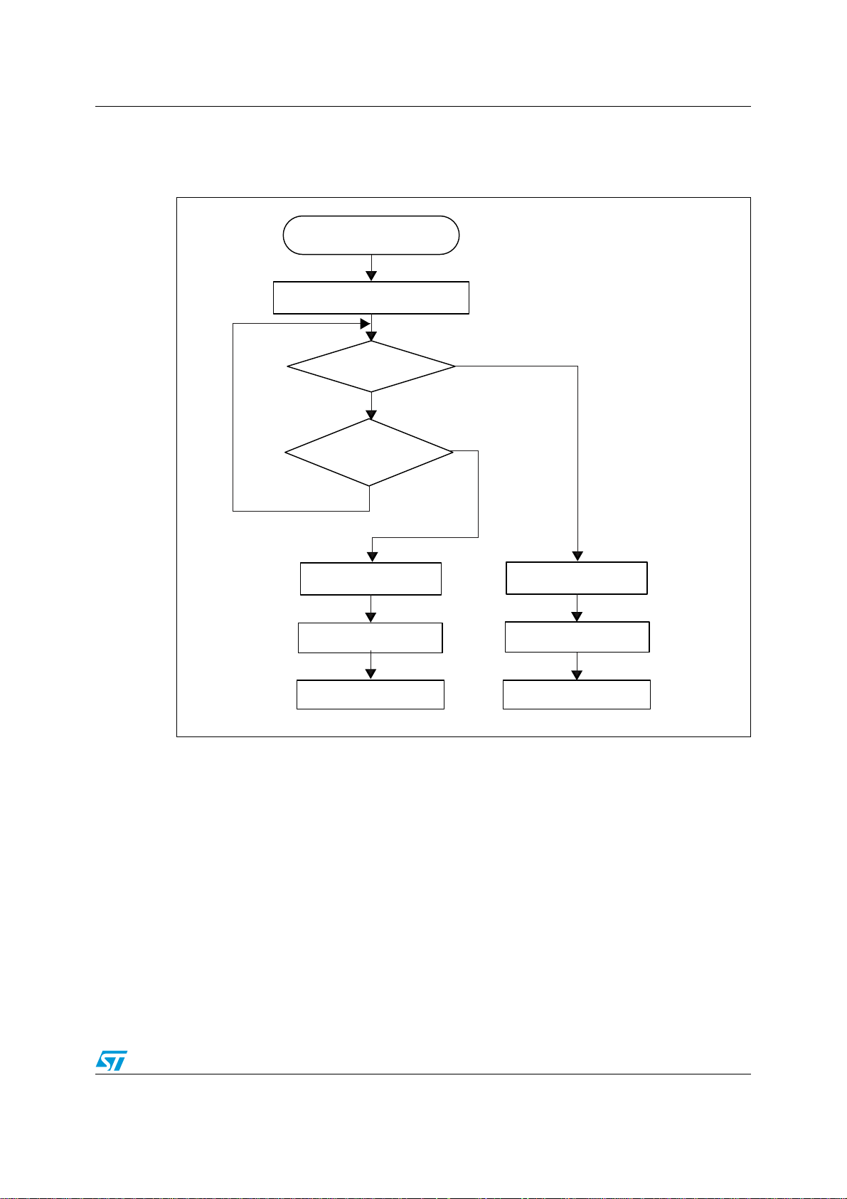
AN2606 STM32F051x6 and STM32F051x8 device bootloader
-36
System Reset
System init (clock, GPIOs, IWDG,
SysTick)
0x7F received
on USART1
YES
NO
0x7F received
on USART2
NO
Disable all interrupt
sources
Configure USART2
Execute BL_USART_Loop
for USART2
YES
Configure USART1
Execute BL_USART_Loop
for USART1
Disable all interrupt
sources
The figure below shows the bootloader detection mechanism. More details are provided in
the sections corresponding to each peripheral bootloader.
Figure 9. Bootloader selection for STM32F051xx
Doc ID 13801 Rev 14 73/88
Page 74

STM32F051x6 and STM32F051x8 device bootloader AN2606
11.4 Important considerations
The bootloader of the STM32F051xx devices has some specific features that should be
taken into consideration, as described below:
● Option byte
Address is 0x1FF8 0000. They allow three levels of protection:
–Level 0
–Level 1
–Level 2
Refer to RM0091 reference manual for more details about protection levels.
● Read protect command corresponds to the Level 1 protection.
● Read unprotect command corresponds to the Level 0 protection.
● Jump to user application
If an application that uses interrupts has to be downloaded to Flash memory address
0x0800 0000 by the Bootloader firmware, then that application must at startup and
before any interrupt is enabled, map the Flash memory by software to the address
0x0000 0000. This can be done by programming the MEM_MODE bits of the
SYSCFG_CFGR1 register (refer to RM0091 reference manual for more details about
software memory mapping).
If the application is loaded into Flash memory at an address different from 0x08000000,
then the vector table has to be mapped to SRAM and the SRAM should in this case be
mapped by software to address 0x0000 0000.
11.5 Bootloader version
The following table lists the STM32F051xx bootloader versions:
Table 26. STM32F051xx bootloader versions
Bootloader
version
number
V2.1 Initial bootloader version
Description Known limitations
When the user application configures a value
of HSI TRIM bits (in RCC_CR register) and
then jumps to the bootloader, the HSITRIM
value is reset to its default value (0) at
Bootloader startup.
74/88 Doc ID 13801 Rev 14
Page 75

AN2606 Device-dependent bootloader parameters
12 Device-dependent bootloader parameters
The bootloader protocol’s command set and sequences for each serial peripheral (USART,
CAN and USB) are the same for all STM32 devices. Some parameters, however, are
device-dependent. For a few commands, the value of some parameters may depend on the
device used. These parameters are listed below:
● PID (product ID), which changes with the device
● Valid memory addresses (RAM, Flash memory, System memory, option byte area)
accepted by the bootloader when the Read Memory, Go and Write Memory commands
are accepted.
● Size of the Flash memory sector used when executing the Write Protect command.
The table below shows the values of these parameters for each STM32 device bootloader in
production.
Table 27. Bootloader device-dependant parameters
Product
Device
Low-density 0x412
Mediumdensity
High-density 0x414
Connectivity
line
Mediumdensity value
line
High-density
value line
XL-density 0x430
Mediumdensity
ultralow power
line
High-density
ultralow power
line
STM32F2xx
devices
(device) IDRAM memory Flash memory Flash sector size
0x410
0x418
0x420
0x428
0x436
0x416
0x411
0x20000200 up
to 0x20002800
0x20000200 up
to 0x20005000
0x20000200 up
to 0x20010000
0x20001000 up
to 0x20010000
0x20000200 up
to 0x20002000
0x20000200 up
to 0x20008000
0x20000800 up
to 0x20018000
0x20001000 up
to 0x2000C000
0x20000800 up
to 0x20004000
0x20002000 up
to 0x20020000
0x08000000 up
to 0x08008000
0x08000000 up
to 0x08020000
0x08000000 up
to 0x08080000
0x08000000 up
to 0x08040000
0x08000000 up
to 0x08020000
0x08000000 up
to 0x08080000
0x08000000 up
to 0x08100000
0x08000000 up
to 0x08060000
0x08000000 up
to 0x08020000
0x08000000 up
to 0x08100000
4 Kbytes (4 pages
of 1 Kbyte each)
4 Kbytes (4 pages
of 1 Kbyte each)
4 Kbytes (2 pages
of 2 Kbytes each)
4 Kbytes (2 pages
of 2 Kbytes each)
4 Kbytes (4 pages
of 1 Kbyte each)
4 Kbytes (2 pages
of 2 Kbytes each)
4 Kbytes (2 pages
of 2 Kbytes each)
4 Kbytes (16
pages of 256
Bytes each)
4 Kbytes (16
pages of 256
Bytes each)
12 sectors
(4x16Kbytes,
1x64Kbytes,
7x128Kbytes)
Option byte
area
0x1FFFF800 0x1FFFF80F
0x1FFFF800 0x1FFFF80F
0x1FFFF800 0x1FFFF80F
0x1FFFF800 0x1FFFF80F
0x1FFFF800 0x1FFFF80F
0x1FFFF800 0x1FFFF80F
0x1FFFF800 0x1FFFF80F
0x1FF80000 0x1FF8000F
0x1FF800000x1FF80020
0x1FFFC0000x1FFFC00F
System
memory
0x1FFFF000 0x1FFFF800
0x1FFFF000 0x1FFFF800
0x1FFFF000 0x1FFFF800
0x1FFFB000 0x1FFFF800
0x1FFFF000 0x1FFFF800
0x1FFFF000 0x1FFFF800
0x1FFFE000 0x1FFFF800
0x1FF00000 0x1FF01000
0x1FF000000x1FF02000
0x1FFF0000 0x1FFF77FF
Doc ID 13801 Rev 14 75/88
Page 76

Device-dependent bootloader parameters AN2606
Table 27. Bootloader device-dependant parameters (continued)
Device
STM32F4xx
devices
STM32F051x6
and
STM32F051x8
devices
Product
(device) IDRAM memory Flash memory Flash sector size
12 sectors
0x413
0x440
0x20002000 up
to 0x20020000
0x20000800 up
to 0x20002000
0x08000000 up
to 0x08100000
0x08000000 up
to 0x08010000
(4x16Kbytes,
1x64Kbytes,
7x128Kbytes)
4 Kbytes (4 pages
of 1 KBytes each)
Option byte
area
0x1FFFC0000x1FFFC00F
0x1FFFF800 -
0x1FFFF80B
System
memory
0x1FFF0000 0x1FFF77FF
0x1FFFEC00 -
0x1FFFF800
76/88 Doc ID 13801 Rev 14
Page 77

AN2606 Bootloader timing characteristics
13 Bootloader timing characteristics
This section presents the main startup timings of the bootloader firmware depending on
products. They can be used to set up the connection timeout, that is how long the host waits
before synchronization with the bootloader is established.
Three types of timings will be described herein:
● Hardware-dependent timings relative to product and directly extracted from the product
datasheet.
● Communication-dependent timings relative to the baudrate and data traffic on the bus.
These timings depend only on the communication interface configuration and on the
host behavior.
● Bootloader software-dependent timings relative to bootloader software operations.
All the timings described in his section are expressed in milliseconds (ms) except when
otherwise specified.
13.1 USART bootloader timing characteristics
Two main timings need to be considered for host operations when using the USART
bootloader:
● Timing A
After bootloader reset, this timing corresponds to the time during which the host waits
before sending the synchronization data (0x7F) to properly configure the bootloader
baudrate detection. This timing will be referred to as A throughout this section.
● Timing B
After sending the synchronization data (0x7F), this timing corresponds to the time
during which the host waits before receiving the first acknowledge response (meaning
that the bootloader is ready to receive and execute host commands). This timing will be
referred to as B throughout this section.
A and B timings are composed of different sub-timings as described in Figure 10.
Doc ID 13801 Rev 14 77/88
Page 78

Bootloader timing characteristics AN2606
$EVICE
2ESET
(OSTSENDS
X&BYTE
(OST2ECEIVES
XBYTE!#+
! "
A
B
C
D E
F FG
2ESET0IN
STATE
"OOTLOADER
EXECUTIONTIME
$EVICE
3TABILIZED
(3)
/.
0,,
3ET
"OOTLOADER
2EADYTORECEIVE
SYNCHRONIZATION
BYTEX&
0,,
,OCKED
$EVICE
RECEIVES
X&BYTE
$EVICE
3ENDS
XBYTE
!#+
2ESET4EMPORIZATIONREFERTO
0,,LOCKTIMEREFERTOPRODUCTDATASHEET
"OOTLOADER
2EADYTORECEIVE
ANDEXECUTE
COMMANDS
!
"
B
C
E
F
G
0ERIODOF4IMETHATHOSTSHOULDWAITAFTERSENDINGTHE
SYNCHRONIZATIONBYTEX&ANDBEFORERECEIVINGTHEACKNOWLEDGE
BYTEX!FTERTHISPERIODTHE"OOTLOADERDEVICEISREADY
TORECEIVEHOSTCOMMANDS
PRODUCTDATASHEET
(3)OSCILLATORSTARTUPTIMEREFER
TOPRODUCTDATASHEET
0ERIODOFTIMETHAT"OOTLOADER
DEVICEFIRMWARENEEDSTOCONFIGURE
PERIPHERALSANDSTARTOPERATIONS
0ERIODOFTIMETHAT"OOTLOADERDEVICEFIRMWARENEEDS
TOCONFIGUREPERIPHERALS
0ERIODOFBYTESENDINGTHROUGH53!24DEPENDSONBAUDRATE
53!24PERIPHERALCONFIGURATIONTIME
X
4HESETIMINGSAREPRODUCTDEPENDENT&ORMOREINFORMATIONREFERTOPRODUCTDATASHEET
X
4HESETIMINGSARECOMMUNICATIONDEPENDENT4HEIRVALUESDEPENDONTHECOMMUNICATIONBAUDRATE
-36
A
D
0ERIODOFTIMETHATHOSTSHOULDWAITAFTERDEVICERESETAND
BEFORESENDINGSYNCHRONIZATIONBYTEX&
Figure 10. USART bootloader timing waveforms
The timing values for each product are listed in Tab le 28 , Tab le 2 9 , Ta bl e 3 0, Ta bl e 3 1 ,
Ta bl e 3 2 , Tab l e 33 , Ta bl e 3 4 , Ta bl e 3 5, and Ta bl e 3 6 .
Table 28. USART bootloader timings for low/medium/high-density and
value line devices
Time Description Min Max Unit
a Reset temporization 1 4.5 ms
b HSI oscillator startup time 0.001 0.002 ms
c Bootloader firmware operations 0.004 - ms
d PLL Lock time 0.2 - ms
e Bootloader firmware operations 0.002 - ms
f One USART byte sending period 0.078125 7.5 ms
g Bootloader firmware operations 0.002 - ms
A Time = a + b + c + d + e 1.207 4.708 ms
B Time = (2 x f) + g 0.15825 15.002 ms
78/88 Doc ID 13801 Rev 14
Page 79

AN2606 Bootloader timing characteristics
Table 29. USART bootloader timings for XL-density line devices
Time Description Min Max Unit
a Reset temporization 1 4.5 ms
b HSI oscillator startup time 0.001 0.002 ms
c Bootloader firmware operations 0.02 - ms
d PLL Lock time 0.2 - ms
e Bootloader firmware operations 0.006 - ms
f One USART byte sending period 0.078125 7.5 ms
g Bootloader firmware operations 0.006 - ms
A Time = a + b + c + d + e 1.227 4.728 ms
B Time = (2 x f) + g 0.16225 15.006 ms
Table 30. USART bootloader timings for connectivity line devices (PA9 pin low)
Time Description Min Max Unit
a Reset temporization 1 4.5 ms
b HSI oscillator startup time 0.001 0.002 ms
c Bootloader firmware operations 0.025 - ms
d PLL Lock time 0.35 - ms
e Bootloader firmware operations 0.02 - ms
f One USART byte sending period 0.078125 7.5 ms
g Bootloader firmware operations 0.007 - ms
A Time = a + b + c + d + e 1.396 4.897 ms
B Time = (2 x f) + g 0.16325 15.007 ms
For connectivity line devices, PA9 pin (USB_VBUS) is used to detect the USB host
connection. The initialization of USB peripheral is performed only if PA9 is high at detection
phase which means that a host is connected to the port and delivering 5 V on the USB bus.
When PA9 level is high at detection phase, more time is required to initialize and shutdown
the USB peripheral.
To minimize bootloader detection time for connectivity line devices when PA9 pin is not
used, keep PA9 state low during detection phase from the moment the device is reset till a
device ACK is sent.
Doc ID 13801 Rev 14 79/88
Page 80
Bootloader timing characteristics AN2606
Table 31. USART bootloader timings for connectivity line devices (PA9 high)
Time Description Min Max Unit
a Reset temporization 1 4.5 ms
b HSI oscillator startup time 0.001 0.002 ms
c Bootloader firmware operations 0.025 - ms
d PLL Lock time 0.35 - ms
e Bootloader firmware operations 523 - ms
f One USART byte sending period 0.078125 7.5 ms
g Bootloader firmware operations 105 - ms
A Time = a + b + c + d + e 524.376 527.877 ms
B Time = (2 x f) + g 105.1563 120 ms
Table 32. USART bootloader timings for STM32L15xx medium-density
ultralow power devices
Time Description Min Max Unit
a Reset temporization 0.4 1.6 ms
b MSI oscillator stabilization time - 0.04 ms
c Bootloader firmware operations 0.064 - ms
d HSI oscillator startup time 0.0037 0.006 ms
e Bootloader firmware operations 0.034 - ms
f One USART byte sending period 0.078125 7.5 ms
g Bootloader firmware operations 0.008 - ms
A Time = a + b + c + d + e 0.5417 1.744 ms
B Time = (2 x f) + g 0.16425 15.008 ms
Table 33. USART bootloader timings for STM32L15xx high-density
ultralow power devices
Time Description Min Max Unit
a Reset Temporization 0.4 1.6 ms
b MSI oscillator stabilization time 0.07 ms
c Bootloader firmware operations 0.058 ms
d HSI oscillator startup time 0.006 ms
e Bootloader firmware operations 0.174 ms
80/88 Doc ID 13801 Rev 14
Page 81

AN2606 Bootloader timing characteristics
Table 33. USART bootloader timings for STM32L15xx high-density
ultralow power devices
f One USART byte sending period 0.078125 7.5 ms
g Bootloader firmware operations 0.0078 ms
A Time = a + b + c + d + e 0.708 1.908 ms
B Time = (2 x f) + g 0.16405 15.0078 ms
Table 34. USART bootloader timings for STM32F205/215xx and
STM32F207/217xx devices
Time Description Min Max Unit
a Reset temporization 0.5 3.0 ms
b HSI oscillator startup time 0.0022 0.004 ms
c Bootloader firmware operations 0.01 - ms
d PLL Lock time 0.075 0.2 ms
e Bootloader firmware operations 84 - ms
f One USART byte sending period 0.078125 7.5 ms
g Bootloader firmware operations 0.009 - ms
A Time = a + b + c + d + e 84.5872 87.214 ms
B Time = (2 x f) + g 0.16525 15.009 ms
Table 35. USART bootloader timings for STM32F405/415xx and
STM32F407/417xx devices
Time Description Min Max Unit
a Reset temporization 0.5 3.0 ms
b HSI oscillator startup time 0.0022 0.004 ms
c Bootloader firmware operations 0.01 - ms
d PLL Lock time 0.075 0.2 ms
e Bootloader firmware operations 84 - ms
f One USART byte sending period 0.078125 7.5 ms
g Bootloader firmware operations 0.009 - ms
A Time = a + b + c + d + e 84.5872 87.214 ms
B Time = (2 x f) + g 0.16525 15.009 ms
Doc ID 13801 Rev 14 81/88
Page 82
Bootloader timing characteristics AN2606
Table 36. USART bootloader timings for STM32F051x6 and STM32F051x8 devices
Time Description Min Max Unit
a Reset Temporization 1.5 4.5 ms
b HSI oscillator startup time 0.001 0.002 ms
c + d + e Bootloader firmware operations 0.111 ms
f One USART byte sending period 0.078125 7.5 ms
g Bootloader firmware operations 0.0095 ms
A Time = a + b + c + d + e 1.612 4.613 ms
B Time = (2 x f) + g 0.16575 15.0095 ms
13.2 USB bootloader timing characteristics
The main timings that need to be considered for host operations when using the USB
bootloader are the following:
● Timing A
After bootloader reset, this timing corresponds to the time during which the host waits
before starting the connection sequence with the device. It is similar to the USART
connection timeout described in Section 13.1. It will be referred to as A throughout this
section.
● Timing B
When the connection sequence has started, this timing corresponds to the time
required by the device to establish a correct connection with the host (meaning that the
bootloader is ready to receive and execute host commands). This timing includes
enumerations and DFU components configuration (e.g. internal Flash memory). This
timing will be referred to as B throughout this section.
For connectivity line devices, if the external HSE crystal frequency is different from 25 MHz
(14.7456 MHz or 8 MHz), the device performs several unsuccessful enumerations (with
connect – disconnect sequences) before being able to establish a correct connection with
the host. This is due to the HSE automatic detection mechanism based on SOF detection.
A and B timings are composed of different sub-timings as described in Figure 11. Refer to
Ta bl e 2 8 , Tab l e 29 , Tab le 3 0, Ta bl e 31 , Tab le 3 2 , Tab le 3 3 , Ta bl e 3 4, Ta bl e 35 , and Tab le 36
for the values of timing A (identical to USART bootloader), and to Ta bl e 3 7 , Tab le 3 8,
Ta bl e 3 9 , and Ta bl e 4 0 for the values of timing B.
Note: For USB interface, only minimum timings are provided since the connection timing
depends on environment and host configuration (number of nodes (hubs), host
speed, traffic on the USB bus, host loading …).
82/88 Doc ID 13801 Rev 14
Page 83
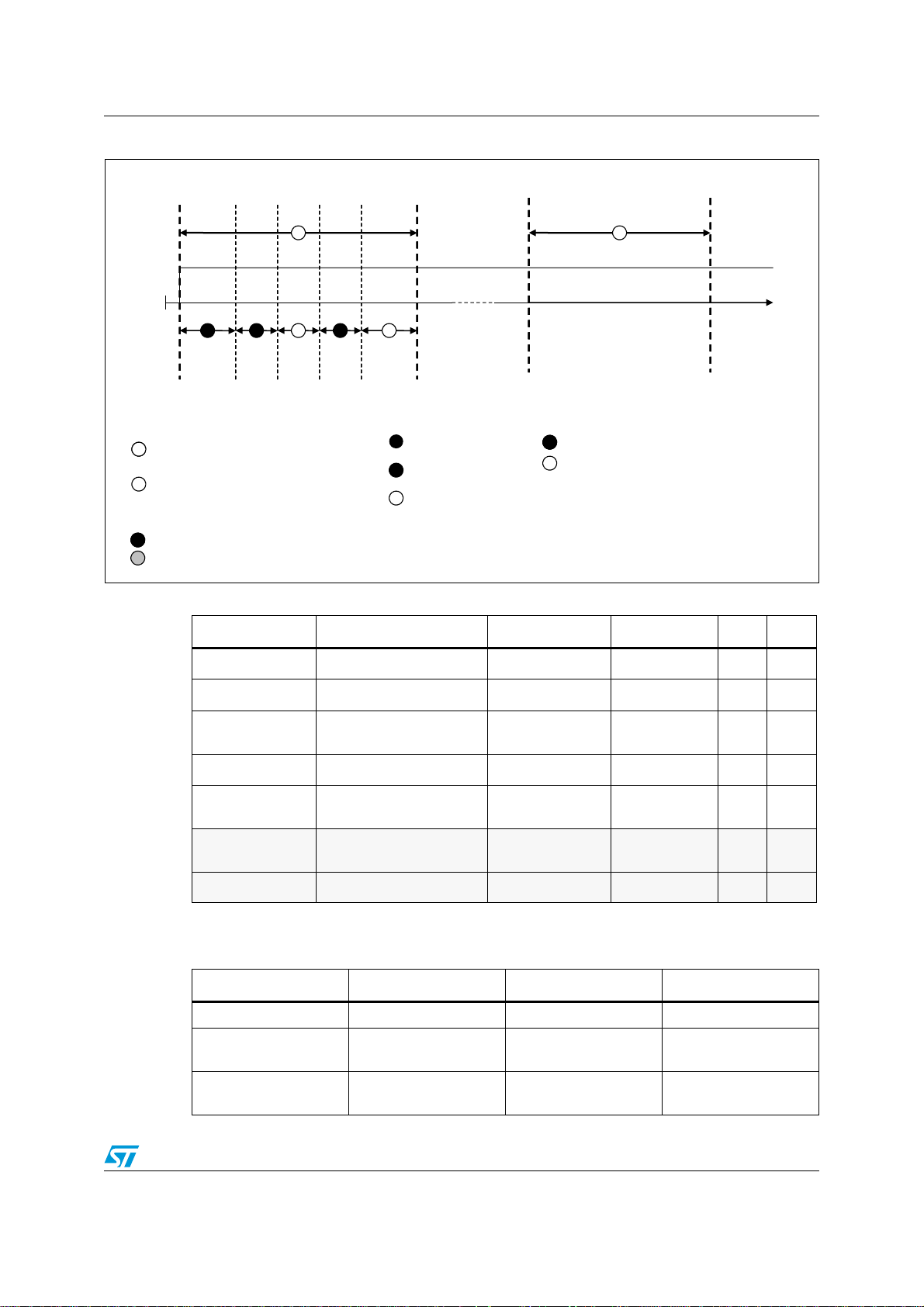
AN2606 Bootloader timing characteristics
$EVICE
2ESET
#ONNECTIONTOHOST
"!
A
B
C
D E
2ESET0IN
STATE
"OOTLOADER
EXECUTIONTIME
53"INITIALIZATIONAND
53"PROTOCOLOPERATIONS
TIME
$EVICE
3TABILIZED
(3)
/.
0,,
3ET
"OOTLOADER
2EADYTOCONNECT
0,,
,OCKED
2ESET4EMPORIZATIONREFERTO
0,,LOCKTIMEREFERTOPRODUCTDATASHEET
"OOTLOADER
2EADYTORECEIVE
ANDEXECUTE
COMMANDS
!
"
B
C
E
0ERIODOF4IMETHATHOSTSHOULD WAITBETWEENSTARTINGCONNECTION
3EQUENCEANDESTABLISHMENTOFCORRECTCONNECTION
!FTERTHISPERIODTHE"OOTLOADERDEVICEISREADY
TORECEIVEHOSTCOMMANDS
PRODUCTDATASHEET
(3)OSCILLATORSTARTUPTIMEREFER
TOPRODUCTDATASHEET
0ERIODOFTIMETHAT"OOTLOADER
DEVICEFIRMWARENEEDSTOCONFIGURE
PERIPHERALSANDSTARTOPERATIONS
0ERIODOFTIMETHAT"OOTLOADERDEVICEFIRMWARENEEDS
TOCONFIGUREPERIPHERALS
X
4HESETIMINGSAREPRODUCTDEPENDENT&ORMOREINFORMATIONREFERTOPRODUCTDATASHEET
X
4HESETIMINGSARECOMMUNICATIONDEPENDENT4HEIRVALUESDEPENDONTHECOMMUNICATIONBAUDRATE
A
D
-36
0ERIODOFTIMETHATHOSTSHOULDWAITAFTERDEVICERESETAND
BEFORESENDINGSYNCHRONIZATIONBYTEX&
Figure 11. USB bootloader timing waveforms
Table 37. USB minimum timings for connectivity line devices
Time Description 25MHz 14.7456MHz 8MHz Unit
a Reset temporization 1 1 1 ms
b HSI oscillator startup time 0.001 0.001 0.001 ms
c
Bootloader firmware
operations
0.025 0.025 0.025 ms
d PLL Lock time 0.35 0.35 0.35 ms
e
A Time = a + b + c + d + e 524.376 524.376
Bootloader firmware
operations
523 523 523 ms
524.3
76
ms
B Connection establishment 460 4500 13700 ms
Table 38. USB minimum timings for STM32L15xx high-density
ultralow power devices
Time Description Min Unit
a Reset Temporization 0.4 ms
b
c
MSI oscillator
stabilization time
Bootloader firmware
operations
0.07 ms
0.058 ms
Doc ID 13801 Rev 14 83/88
Page 84
Bootloader timing characteristics AN2606
Table 38. USB minimum timings for STM32L15xx high-density
ultralow power devices (continued)
Time Description Min Unit
d
e
A
B
Table 39. USB minimum timings for STM32F205/215xx,
HSI oscillator startup
time
Bootloader firmware
operations
Time = a + b + c + d +
e
Connection
establishment
0.0037 ms
0.174 ms
0.7057 ms
849 ms
and STM32F207/217xx devices
Time Description Min Unit
a Reset temporization 0.5 ms
b HSI oscillator startup time 0.0022 ms
c Bootloader firmware operations 0.01 ms
d PLL Lock time 0.075 ms
e Bootloader firmware operations 84 ms
A Time = a + b + c + d + e 84.5872 ms
B Connection establishment 54 ms
Table 40. USB minimum timings for STM32F405/415xx,
and STM32F407/417xx devices
Time Description Min Unit
a Reset temporization 0.5 ms
b HSI oscillator startup time 0.0022 ms
c Bootloader firmware operations 0.01 ms
d PLL Lock time 0.075 ms
e Bootloader firmware operations 84 ms
A Time = a + b + c + d + e 84.5872 ms
B Connection establishment 54 ms
For the STM32F2xx and STM32F4xx devices bootloader, the timing values are independent
from the HSE crystal frequency. The detection of the HSE crystal frequency value is
performed through period measurement using TIM11 timer and HSI internal oscillator.
84/88 Doc ID 13801 Rev 14
Page 85

AN2606 Revision history
14 Revision history
.
Table 41. Document revision history
Date Revision Changes
22-Oct-2007 1 Initial release.
All STM32 in production (rev. B and rev. Z) include the bootloader
described in this application note.
Modified: Section 3.1: Bootloader activation and Section 1.4:
Bootloader code sequence.
Added: Section 1.3: Hardware requirements, Section 1.5: Choosing
22-Jan-2008 2
26-May-2008 3
29-Jan-2009 4
the USART baud rate, Section 1.6: Using the bootloader and
Section 3.2: Exiting System memory boot mode.
Note 2 linked to Get, Get Version & Read Protection Status and Get
ID commands in Table 3: Bootloader commands, Note 3 added.
Notion of “permanent” (Permanent Write Unprotect/Readout
Protect/Unprotect) removed from document. Small text changes.
Bootloader version upgraded to 2.0.
Small text changes. RAM and System memory added to Ta bl e 4:
STM32F10xxx configuration in System memory boot mode.
Section 1.6: Using the bootloader on page 8 removed.
Erase modified, Note 3 modified and Note 1 added in Ta bl e 3 :
Bootloader commands on page 9.
Byte 3: on page 11 modified.
Byte 2: on page 13 modified.
Byte 2:, Bytes 3-4: and Byte 5: on page 15 modified, Note 3
modified.
Byte 8: on page 18 modified.
Notes added to Section 2.5: Go command on page 18.
Figure 11: Go command: device side on page 20 modified.
Note added in Section 2.6: Write Memory command on page 21.
Byte 8: on page 24 modified.
Figure 14: Erase Memory command: host side and Figure 15: Erase
Memory command: device side modified.
Byte 3: on page 26 modified.
Table 3: Bootloader commands on page 9.
Note modified and note added in Section 2.8: Write Protect
command on page 27.
Figure 16: Write Protect command: host side, Figure 17: Write
Protect command: device side, Figure 19: Write Unprotect
command: device side, Figure 21: Readout Protect command:
device side and Figure 23: Readout Unprotect command: device
side modified.
This application note also applies to the STM32F102xx
microcontrollers.
Bootloader version updated to V2.2 (see Table 4: Bootloader
versions).
Doc ID 13801 Rev 14 85/88
Page 86

Revision history AN2606
Table 41. Document revision history (continued)
Date Revision Changes
IWDG added to Table 4: STM32F10xxx configuration in System
memory boot mode. Note added.
BL changed bootloader in the entire document.
Go command description modified in Table 4: STM32F10xxx
configuration in System memory boot mode.
Number of bytes awaited by the bootloader corrected in Section 2.4:
Read Memory command.
Note modified below Figure 10: Go command: host side.
19-Nov-2009 5
09-Mar-2010 6
20-Apr-2010 7
08-Oct-2010 8
Note removed in Section 2.5: Go command and note added.
Start RAM address specified and note added in Section 2.6: Write
Memory command. All options are erased when a Write Memory
command is issued to the Option byte area.
Figure 11: Go command: device side modified.
Figure 13: Write Memory command: device side modified.
Note added and bytes 3 and 4 sent by the host modified in
Section 2.7: Erase Memory command.
Note added to Section 2.8: Write Protect command.
Application note restructured. Value line and connectivity line device
bootloader added (Replaces AN2662).
Introduction changed. Glossary added.
Related documents: added XL-density line datasheets and
programming manual.
Glossary: added XL-density line devices.
Ta bl e 3: added information for XL-density line devices.
Section 4.1: Bootloader configuration: updated first sentence.
Section 5.1: Bootloader configuration: updated first sentence.
Added Section 6: STM32F101xx and STM32F103xx XL-density
device bootloader.
Ta bl e 2 7: added information for XL-density line devices.
Added information for high-density value line devices in Tab l e 3 and
Ta bl e 2 7.
14-Oct-2010 9 Removed references to obsolete devices.
26-Nov-2010 10 Added information on ultralow power devices.
Added information related to STM32F205/215xx and
13-Apr-2011 11
06-Jun-2011 12
86/88 Doc ID 13801 Rev 14
STM32F207/217xx devices.
Added Section 13: Bootloader timing characteristics
Updated:
– Table 12: STM32L15xxx bootloader versions
– Table 16: STM32F2xx configuration in System memory boot mode
– Table 18: STM32F2xx bootloader V2.x versions
– Table 21: STM32F2xx bootloader V3.x versions
Page 87

AN2606 Revision history
Table 41. Document revision history (continued)
Date Revision Changes
Added information related to STM32F405/415xx and
STM32F407/417xx bootloader, and STM32F105xx/107xx bootloader
28-Nov-2011 13
30-Jul-2012 14
V2.1.
Added value line devices in Section 4: STM32F100xx,
STM32F101xx, STM32F102xx, STM32F103xx, medium-density and
high-density value line bootloader title and overview.
Added information related to STM32F051x6/STM32F051x8 and to
High-density ultralow power STM32L151xx, STM32L152xx
bootloader.
Added case of BOOT1 bit in Section 3.1: Bootloader activation.
Updated Connectivity line, High-density ultralow power line,
STM32F2xx and STM32F4xx in Table 3: Embedded bootloaders.
Added bootloader version V2.2 in Table 7: STM32F105xx and
STM32F107xx bootloader versions.
Added bootloader V2.2 in Section 5.4.1: How to identify
STM32F105xx/107xx bootloader versions.
Added note related to DFU interface below Table 14: STM32L1xx
High-density configuration in System memory boot mode. Added
V4.2 bootloader know limitations and updated description, and
added V4.5 bootloader in Table 15: STM32L1xx High-density
bootloader versions.
Added note related to DFU interface below Table 19: STM32F2xx
configuration in System memory boot mode. Added V3.2 bootloader
know limitations, and added V3.3 bootloader in Ta bl e 2 1:
STM32F2xx bootloader V3.x versions. Updated STM32F2xx and
STM32F4xx system memory end address in Table 22: STM32F4xx
configuration in System memory boot mode.
Added note related to DFU interface below Table 22: STM32F4xx
configuration in System memory boot mode. Added V3.0 bootloader
know limitations, and added V3.1 bootloader in Ta bl e 2 4:
STM32F4xx bootloader version.
Added bootloader V2.1 know limitations in Table 26: STM32F051xx
bootloader versions.
Updated STM32F051x6/x8 system memory end address in Table 27:
Bootloader device-dependant parameters.
Added Table 33: USART bootloader timings for STM32L15xx high-
density ultralow power devices, and Table 36: USART bootloader
timings for STM32F051x6 and STM32F051x8 devices.
Added Table 38: USB minimum timings for STM32L15xx high-
density ultralow power devices.
Doc ID 13801 Rev 14 87/88
Page 88

AN2606
Please Read Carefully:
Information in this document is provided solely in connection with ST products. STMicroelectronics NV and its subsidiaries (“ST”) reserve the
right to make changes, corrections, modifications or improvements, to this document, and the products and services described herein at any
time, without notice.
All ST products are sold pursuant to ST’s terms and conditions of sale.
Purchasers are solely responsible for the choice, selection and use of the ST products and services described herein, and ST assumes no
liability whatsoever relating to the choice, selection or use of the ST products and services described herein.
No license, express or implied, by estoppel or otherwise, to any intellectual property rights is granted under this document. If any part of this
document refers to any third party products or services it shall not be deemed a license grant by ST for the use of such third party products
or services, or any intellectual property contained therein or considered as a warranty covering the use in any manner whatsoever of such
third party products or services or any intellectual property contained therein.
UNLESS OTHERWISE SET FORTH IN ST’S TERMS AND CONDITIONS OF SALE ST DISCLAIMS ANY EXPRESS OR IMPLIED
WARRANTY WITH RESPECT TO THE USE AND/OR SALE OF ST PRODUCTS INCLUDING WITHOUT LIMITATION IMPLIED
WARRANTIES OF MERCHANTABILITY, FITNESS FOR A PARTICULAR PURPOSE (AND THEIR EQUIVALENTS UNDER THE LAWS
OF ANY JURISDICTION), OR INFRINGEMENT OF ANY PATENT, COPYRIGHT OR OTHER INTELLECTUAL PROPERTY RIGHT.
UNLESS EXPRESSLY APPROVED IN WRITING BY TWO AUTHORIZED ST REPRESENTATIVES, ST PRODUCTS ARE NOT
RECOMMENDED, AUTHORIZED OR WARRANTED FOR USE IN MILITARY, AIR CRAFT, SPACE, LIFE SAVING, OR LIFE SUSTAINING
APPLICATIONS, NOR IN PRODUCTS OR SYSTEMS WHERE FAILURE OR MALFUNCTION MAY RESULT IN PERSONAL INJURY,
DEATH, OR SEVERE PROPERTY OR ENVIRONMENTAL DAMAGE. ST PRODUCTS WHICH ARE NOT SPECIFIED AS "AUTOMOTIVE
GRADE" MAY ONLY BE USED IN AUTOMOTIVE APPLICATIONS AT USER’S OWN RISK.
Resale of ST products with provisions different from the statements and/or technical features set forth in this document shall immediately void
any warranty granted by ST for the ST product or service described herein and shall not create or extend in any manner whatsoever, any
liability of ST.
ST and the ST logo are trademarks or registered trademarks of ST in various countries.
Information in this document supersedes and replaces all information previously supplied.
The ST logo is a registered trademark of STMicroelectronics. All other names are the property of their respective owners.
© 2012 STMicroelectronics - All rights reserved
STMicroelectronics group of companies
Australia - Belgium - Brazil - Canada - China - Czech Republic - Finland - France - Germany - Hong Kong - India - Israel - Italy - Japan -
Malaysia - Malta - Morocco - Philippines - Singapore - Spain - Sweden - Switzerland - United Kingdom - United States of America
www.st.com
88/88 Doc ID 13801 Rev 14
 Loading...