

Page 1

AN2592
Application note
How to achieve 32-bit timer resolution using the link system
in STM32F10x microcontrollers
Introduction
In many applications, 32-bit resolution is required to measure external signal periods of up
to several hundreds of seconds or, to generate delays or periodic signals with large periods.
The STM32F10x microcontrollers offer the possibility of chaining two 16-bit timers to obtain
a 32-bit resolution based on a specific configuration of the timers and on the use of the timer
link system.
This application note gives general guidelines to emulate a 32-bit timer. The two basic
operating modes, that is the input capture mode and the output compare mode, are
presented. Each mode is treated independently and, each time, examples of applications
are provided.
January 2011 Doc ID 13711 Rev 2 1/17
www.st.com
Page 2

Contents AN2592
Contents
1 STM32F10x timer synchronization . . . . . . . . . . . . . . . . . . . . . . . . . . . . . 5
1.1 Timer link system presentation . . . . . . . . . . . . . . . . . . . . . . . . . . . . . . . . . . 5
1.2 How to synchronize two timers using the link system . . . . . . . . . . . . . . . . 5
2 32-bit input capture timer resolution . . . . . . . . . . . . . . . . . . . . . . . . . . . . 7
2.1 Principle . . . . . . . . . . . . . . . . . . . . . . . . . . . . . . . . . . . . . . . . . . . . . . . . . . . 7
2.2 Timer configuration . . . . . . . . . . . . . . . . . . . . . . . . . . . . . . . . . . . . . . . . . . . 7
2.2.1 TIM3 master configuration . . . . . . . . . . . . . . . . . . . . . . . . . . . . . . . . . . . . 8
2.2.2 TIM2 slave configuration . . . . . . . . . . . . . . . . . . . . . . . . . . . . . . . . . . . . . 9
2.2.3 Master and slave synchronization . . . . . . . . . . . . . . . . . . . . . . . . . . . . . . 9
3 32-bit output compare timer resolution . . . . . . . . . . . . . . . . . . . . . . . . 10
3.1 Principle and timer configuration . . . . . . . . . . . . . . . . . . . . . . . . . . . . . . . 10
3.2 Output compare mode configuration . . . . . . . . . . . . . . . . . . . . . . . . . . . . 12
3.2.1 Output compare active mode example . . . . . . . . . . . . . . . . . . . . . . . . . 12
3.2.2 Output compare toggle mode example . . . . . . . . . . . . . . . . . . . . . . . . . 14
4 Revision history . . . . . . . . . . . . . . . . . . . . . . . . . . . . . . . . . . . . . . . . . . . 16
2/17 Doc ID 13711 Rev 2
Page 3

AN2592 List of tables
List of tables
Table 1. Document revision history . . . . . . . . . . . . . . . . . . . . . . . . . . . . . . . . . . . . . . . . . . . . . . . . . 16
Doc ID 13711 Rev 2 3/17
Page 4

List of figures AN2592
List of figures
Figure 1. Simplified TIM2 trigger controller block. . . . . . . . . . . . . . . . . . . . . . . . . . . . . . . . . . . . . . . . . 5
Figure 2. Timer synchronization in input capture mode . . . . . . . . . . . . . . . . . . . . . . . . . . . . . . . . . . . . 8
Figure 3. Timer synchronization in output compare mode . . . . . . . . . . . . . . . . . . . . . . . . . . . . . . . . . 11
Figure 4. TIM2 output signals . . . . . . . . . . . . . . . . . . . . . . . . . . . . . . . . . . . . . . . . . . . . . . . . . . . . . . 13
Figure 5. TIM2 output signals . . . . . . . . . . . . . . . . . . . . . . . . . . . . . . . . . . . . . . . . . . . . . . . . . . . . . . 15
Figure 6. TIM2 Channel1 output signal . . . . . . . . . . . . . . . . . . . . . . . . . . . . . . . . . . . . . . . . . . . . . . . 15
4/17 Doc ID 13711 Rev 2
Page 5
AN2592 STM32F10x timer synchronization
TIMxCLK
ETR
TRG01
TRG03
TRG04
ITR0
ITR2
ITR3
TIM2
Trigger
controller
TRG0 TRG02
TI1FP1
TI2FP2
ai14603
1 STM32F10x timer synchronization
1.1 Timer link system presentation
In the STM32F10x microcontrollers, the embedded timers can be linked together for timer
synchronization or chaining purposes.
Using the timer link system, a timer configured in Master mode can:
● reset the counter of the slave timer
● start and/or stop the slave timer counter
● clock the slave timer counter
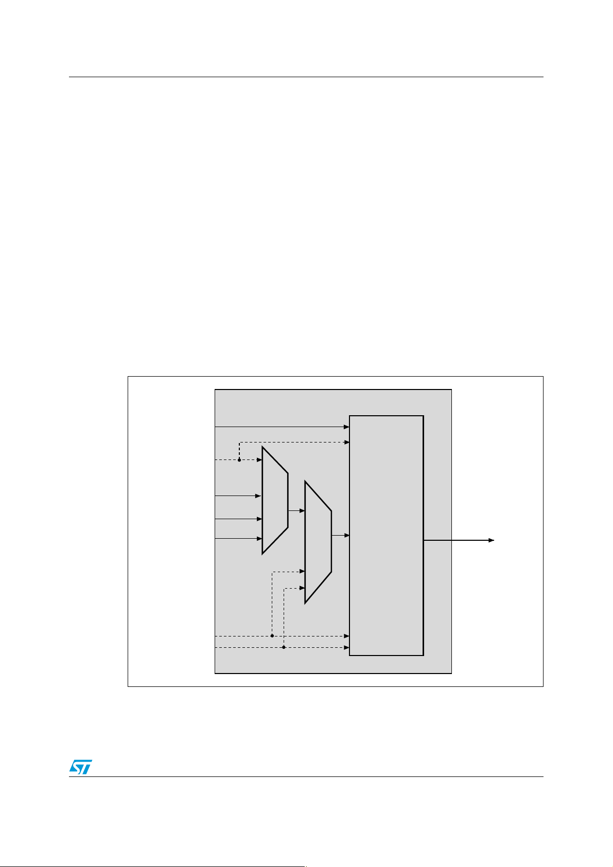
1.2 How to synchronize two timers using the link system
In addition to the TIMx_CHx pins, timers have several internal triggers that are
indispensable for linking and chaining operation.
Figure 1 shows a simplified representation of the timer block, that highlights the internal
triggers. TIM2 is used as an example.
Figure 1. Simplified TIM2 trigger controller block
The internal triggers (ITR0, ITR2 and ITR3) are used when TIM2 is configured in the Slave
mode. They then determine which master controls TIM2.
Doc ID 13711 Rev 2 5/17
Page 6

STM32F10x timer synchronization AN2592
For example, if TIM2 uses ITR2 as an internal trigger, this means that TIM2 is synchronized
with TIM3.
These triggers can be easily redirected to the master by setting the right combination of TS
bits in the SMCR register.
The trigger output, TRGO, is used when TIM2 is configured in the Master mode. It then
determines which events or signals is sent to the slave timers for synchronization.
Different events or signals can be transmitted to the slave, as listed below. They are selected
using the MMS bits in the CR2 register.
● reset event
● enable event
● update event
● compare pulse
● OCxREF where x is 1, 2, 3 or 4.
Once the master trigger output, TRGO, and the slave’s internal triggers, ITRx, are
configured, the two timers are chained.
There are four different slave modes that are selected using the SMS bits in the SMCR
register. They are the following:
● Reset mode: in this mode, the rising edge of the trigger signal reinitializes the counter
and generates an update of the registers.
● Gated mode: the slave counter start and stop are both controlled by the high level on
the trigger input.
● Trigger mode: the start of the slave counter is controlled by the rising edge of the trigger
input signal.
● External clock mode1: the slave counter is clocked by the rising edges of the selected
trigger input signal.
6/17 Doc ID 13711 Rev 2
Page 7

AN2592 32-bit input capture timer resolution
F
TIMxCLK
ARR
-------------------------- -
72 10
6
×
0xFFFF
----------------------- - 1098 Hz===
2 32-bit input capture timer resolution
2.1 Principle
To measure the period of an external signal, the timer can be used in input capture mode.
The maximum frequency, that can be measured with the 16-bit timer, depends on the
TIMxCLK signal.
For example, if the timer is clocked by 72 MHz (TIMxCLK = 72 MHz), the minimum
frequency F that can be measured is:
In some applications, the user needs to measure large periods. The idea is to increase the
timer resolution from 16-bit to 32-bit using a specific configuration based on the timer link
system.
2.2 Timer configuration
The measure is performed by two timers synchronized in a specific mode. The master
measures the LSB part of the external signal period/frequency and the slave measures the
MSB part. The two timers are used in input capture mode.
Figure 2 further explains the typical internal connection of the master and slave timers. TIM3
is used as the master for the TIM2 timer.
Doc ID 13711 Rev 2 7/17
Page 8

32-bit input capture timer resolution AN2592
TIMxCLK
ETR
TRG01
TRG03
TRG04
ITR0
ITR2
ITR3
TIM2
Trigger
controller
TRG0
TI1FP1
TI2FP2
Input filter &
edge detector
16-bit CCR1 register
ITR0
ITR1
ITR3
TIM3
Trigger
controller
TRG0
TI1FP1
TI2FP2
Input filter &
edge detector
16-bit CCR1 register
TI1
TI1
External signal
TIMxCLK
TRG02
ai14604
Figure 2. Timer synchronization in input capture mode
2.2.1 TIM3 master configuration
The master timer is used to measure the LSB part of the external period or frequency. To do
so, it is configured as follows:
● no prescaler is used
● the external signal is connected to channel 1 and the rising edge is configured as the
active edge.
The input capture module is used to latch the value of the counter after a transition detected
by the corresponding input channel. To get the external signal period, two consecutive
8/17 Doc ID 13711 Rev 2
captures are needed and the period is calculated by subtracting these two values.
To avoid this method and facilitate the input capture measurement, the master counter is
reset after each rising edge detected on the timer input channel by:
● selecting TI1FP1 as the input trigger by setting the TS bits in the SMCR register
● selecting the reset mode as the slave mode by configuring the SMS bits in the SMCR
register
Using this configuration, when an edge is detected, the counter is reset and the period of
the external signal is automatically given by the value on the CCR1 register.
Page 9

AN2592 32-bit input capture timer resolution
ExtSignalFreq
72 106×
MS B 65535 LS B+×
------------------------------------------------------- -=
2.2.2 TIM2 slave configuration
The slave timer is used to measure the MSB part of the external frequency. To do so, it is
configured as follows:
● prescaler is fixed to 0xFFFF
● the external signal is connected to channel 1 and the rising edge is configured as the
active edge.
2.2.3 Master and slave synchronization
Master configuration
● Use the master update event as the master trigger output (TRGO)
● Enable the Master/Slave mode.
Slave configuration
● Select the slave input trigger: the master trigger output (TRGO) used as the input
trigger for the slave.
● Enable the Master/Slave mode
● Use the external clock mode 1 as the Slave mode: the slave is clocked by the update
event of the master timer. That is, when the master counter is overflow, the slave
counter is incremented.
Using this configuration, each time the period to be measured exceeds the 16-bit master
timer Auto-reload register, an update event is generated to clock the slave timer.
When the active edge is detected on the master and slave timer inputs, the two counter
values are copied into the master CCR1 register and the slave CCR1 register, respectively.
Since the slave is clocked by the master update event, the number of master overflow is
recorded by the slave as the MSB part of the 32-bit input capture register, the LSB is read
on the Master CCR1.
The external signal frequency is calculated on each master input capture interrupt as
follows:
LSB is the master capture compare register value (LSB = TIM3->CCR1 register value).
To get the MSB value, two consecutive captures are needed and the MSB variable is
calculated by subtracting these two values as shown below:
If MSB1 > MSB2 then MSB = 0xFFFF – ((MSB1 – MSB2)) – 1
If MSB1 < MSB2 then MSB = (MSB2 – MSB1) – 1
MSB1 and MSB2 are given by the slave capture compare value (TIM2->CCR2 register
value).
Since the master timer is used in Reset mode, when the active edge is detected on the
master timer, the counter is reinitialized and an update is generated. To avoid this additional
update event, 1 is subtracted from the MSB value.
Using this method, the maximum frequency that can be measured, with TIMxCLK equal to
72 MHz, is 17 mHz instead of 1098 Hz when a 16-bit timer is used.
Doc ID 13711 Rev 2 9/17
Page 10

32-bit output compare timer resolution AN2592
3 32-bit output compare timer resolution
3.1 Principle and timer configuration
The idea is to use two timers to generate a 32-bit resolution output compare signal; one
timer that gives the MSB, and the other that provides the LSB of the 32-bit output compare
signal.
Compare pulse is one of the master modes offered by the STM32F10x timers. With the
Compare pulse mode selected, each time the CC1IF flag is to be set, that is, as soon as
there is a compare match, the master trigger output (TRGO) sends a positive pulse.
In addition, if the timer master is being used in output compare mode, the LSB or MSB part
of the 32-bit output compare signal is loaded into the master CCRx register. When the
counter of the master reaches the loaded value, it triggers the other timer, causing it to
generate the missing MSB or LSB.
To generate the MSB or the LSB part of the output compare signal, the slave timer must wait
for the master trigger output signal and then start counting in order to introduce the missing
16-bit (LSB or MSB) part. For this, the slave timer has to be configured in the one-pulse
mode (OPM).
The one-pulse mode is a particular case of the input capture and output compare modes. It
allows the counter to be started in response to a stimulus, and to generate a pulse with a
programmable length after a programmable delay.
The counter start can be controlled through the slave mode controller and the waveform can
be generated in output compare mode. If the one-pulse mode (OPM) is selected by setting
the OPM bit in the CR1 register, the counter stops automatically at the next update event.
The STM32F10x timers offer the possibility of redirecting the internal trigger (ITR) and to
use it as the input signal for the capture/compare array. In this case, the internal trigger can
be used as a stimulus for a slave timer initially configured in one-pulse mode (OPM). This is
done by configuring the CCxS bits in the CCMRx register to be mapped on TRC.
This configuration allows the cascading of two timers to obtain a 32-bit time base resolution.
Figure 3 explains how the two timers are cascaded.
10/17 Doc ID 13711 Rev 2
Page 11

AN2592 32-bit output compare timer resolution
TIMxCLK
ETR
TRG01
TRG03
TRG04
ITR0
ITR2
ITR3
TIM2
Trigger
controller
TRGO
ITR0
ITR1
ITR3
TIM3
Trigger
controller
TRGO
TI1FP1
TI2FP2
TIMxCLK
TRG02
ai14605
OCx
CCxI
OCx
CCxI
TRC
OCx
Input filter &
edge detector
Prescaler
16-bit CCRx
register
16-bit CCRx
register
16-bit CCRx
register
Figure 3. Timer synchronization in output compare mode
TIM3 is the master timer used in output compare mode and the trigger output (TRGO3)
sends a positive pulse when the CC1IF flag is to be set as soon as a compare match
occurs.
To connect the TRGO3 output of TIM3 to TIM2, TIM2 must be configured in slave mode
using ITR2 as the internal trigger.
Then the slave mode controller is configured in trigger mode. This causes the TIM2 counter
to be started at a rising edge of the TIM3 trigger signal (that corresponds to the TIM3
compare match).
The two timers are configured as described below:
TIM3 master configuration
● configure TIM3 in output compare mode, the CCRx register must be loaded with the
LSB or the MSB part of the signal
● use the timer master compare pulse event as the trigger output (TRGO)
● set the prescaler value
● enable the master/slave mode
Doc ID 13711 Rev 2 11/17
Page 12

32-bit output compare timer resolution AN2592
TIM2 slave configuration
● TIM2 is used in one-pulse mode, so there are three steps of configuration:
– the input capture module
– the output compare module and the trigger controller
– and the synchronization part
● to configure the TIM2 timer the user has to:
– map TRC onto TIx by writing CCxS = '11' into the TIMx_CCMRx register
– configure ITR2 as the trigger for the slave mode controller (TRGI) by writing
TS = '010' in the TIMx_SMCR register
– use the trigger mode as the slave mode by writing SMS to '110' in the
TIMx_SMCR register: the counter start is controlled by the master
– configure the output compare mode by setting the right combination of the OCxM
bits in the TIMx_CCMRx register (OCxM can be set to '000', '001', '010' or '011').
The CCRx register must be loaded with the MSB or the LSB part
– set the prescaler value
– select the output pin by configuring the CCxS bits in the TIMx_CCMRx register
– enable the one-pulse mode by setting the bit OPM in the TIMx_CR1 register. This
causes the counter to stop at the next update event. So the counter start is
controlled by the master but the stop is controlled by the counter itself.
3.2 Output compare mode configuration
3.2.1 Output compare active mode example
Master configuration
TIM3 is used as the master timer in output compare active mode. TIM3CLK is equal to
72 MHz, no prescaler is used, so the TIM3 counter clock is equal to:
TIM3 counter clock = TIM3CLK/(prescaler + 1) = 72 MHz
TIM3 generates the LSB part of the 32 bit output compare delay, and this delay value is
loaded into the CCR1 register.
Slave configuration
TIM2 is used as the slave timer in one-pulse mode as described below:
● channel1, channel2 and channel3 are used in output compare active mode. The
corresponding CCRx registers are loaded with the MSB part
● channel4 is used in input capture mode: CC4S is connected to TRC
● the prescaler is set to 0xFFFF
● the trigger mode is used as the slave mode
TIM2 is a slave for TIM3 so ITR2 is used as the internal trigger (TS = ‘010’ in TIM2_SMCR
register).
In one-pulse mode, the edge detection on TIM2 IC4 (TRC) sets the TIM2 counter enable
(CEN) bit, which enables the counter.
12/17 Doc ID 13711 Rev 2
Page 13

AN2592 32-bit output compare timer resolution
CC1 delay
MSB1 65536× LSB+
72 10
6
×
-----------------------------------------------------------=
CC1 delay 44.74 s=
CC2 delay
MSB2 65536× LSB+
72 10
6
×
--------------------------------------------------------- -=
CC2 delay 37.28 s=
CC3 delay
MSB3 65536× LSB+
72 10
6
×
--------------------------------------------------------- -=
CC3 delay 29.82 s=
When a match is found between the capture/compare register and the counter, the output
compare function assigns the corresponding output pin with a programmable value
determined by the output compare mode and the output polarity. In this example, after the
programmed delays, the TIM2 pins are set to their active mode.
In this example, the three capture compare register values are TIM2_CCR1 = MSB1 =
0xC000, TIM2_CCR2 = MSB2 = 0xA000 and TIM2_CCR3 = MSB3 = 0x8000, respectively.
TIM3_CCR1 = LSB = 0x8534.
The equations of the TIM2 output compare delays are given below and shown in Figure 4.
, which gives .
, which gives .
, which gives
Note: The same configuration steps are used for the output compare inactive mode. The user only
needs to place TIM2 in output compare inactive mode instead of output compare active
mode, and then to go through the same steps.
Figure 4 shows the three signals.
Figure 4. TIM2 output signals
Doc ID 13711 Rev 2 13/17
Page 14

32-bit output compare timer resolution AN2592
CC1 delay
MSB 65536 LS B1+×
72 10
6
×
-----------------------------------------------------------=
CC1 delay 1.25 ms=
CC2 delay
MSB 65536 LS B2+×
72 10
6
×
-----------------------------------------------------------=
CC2 delay 1.48 ms=
CC3 delay
MSB 65536 LS B3+×
72 10
6
×
-----------------------------------------------------------=
CC3 delay 1.76 ms=
3.2.2 Output compare toggle mode example
Master configuration
TIM3 is used as the master timer in output compare toggle mode. TIM3CLK is equal to
72 MHz, The prescaler is set to 0xFFFF.
TIM3 generates the MSB part of the 32-bit output compare delay, and this delay value is
loaded into the CCR1 register.
Slave configuration
TIM2 is used as the slave timer in one-pulse mode as described below:
● channel 1, channel2 and channel3 are used in output compare toggle mode. The
corresponding CCRx registers are loaded with the LSB part
● channel4 is used in input capture mode: CC4S is connected to TRC
● the prescaler is set to 0x0
● the trigger mode is used as the slave mode
TIM2 is a slave for TIM3 so ITR2 is used as the internal trigger (TS = ‘010’ in TIM2_SMCR
register).
In one-pulse mode, the edge detection on TIM2 IC4 (TRC) sets the TIM2 counter enable
(CEN) bit, which enables the counter.
When a match is found between the capture/compare register and the counter, the output
compare function assigns the corresponding output pin with a programmable value
determined by the output compare mode and the output polarity. In this example, when the
match is found between the counter and the TIM2_CCRx registers, the TIM2 pins toggle
and capture compare interrupts are generated. In the corresponding routine, the
TIM2_CCRx registers are updated in order to have three periodic signals with three different
frequencies.
In this example, the three capture compare register values are TIM2_CCR1 = LSB1 =
0x5FFF, TIM2_CCR2 = LSB2 = 0x9FFF and TIM2_CCR3 = LSB3 = 0xEFFF, respectively.
TIM3_CCR1 = MSB = 0x1.
, which gives: .
, which gives: .
, which gives: .
Note: The same configuration steps are used for the output compare timing mode. The user only
needs to place TIM2 in output compare timing mode instead of output compare toggle
mode, and then to go through the same steps.
Figure 5 shows the three signals.
14/17 Doc ID 13711 Rev 2
Page 15

AN2592 32-bit output compare timer resolution
Figure 5. TIM2 output signals
Figure 6 shows the maximum delay with the following configuration: MSB = LSB1 = 0xFFFF.
Figure 6. TIM2 Channel1 output signal
Doc ID 13711 Rev 2 15/17
Page 16

Revision history AN2592
4 Revision history
Table 1. Document revision history
Date Revision Changes
31-Aug-2007 1 Initial release.
11-Jan-2011 2 Changed part number references to STM32F10x.
16/17 Doc ID 13711 Rev 2
Page 17

AN2592
Please Read Carefully:
Information in this document is provided solely in connection with ST products. STMicroelectronics NV and its subsidiaries (“ST”) reserve the
right to make changes, corrections, modifications or improvements, to this document, and the products and services described herein at any
time, without notice.
All ST products are sold pursuant to ST’s terms and conditions of sale.
Purchasers are solely responsible for the choice, selection and use of the ST products and services described herein, and ST assumes no
liability whatsoever relating to the choice, selection or use of the ST products and services described herein.
No license, express or implied, by estoppel or otherwise, to any intellectual property rights is granted under this document. If any part of this
document refers to any third party products or services it shall not be deemed a license grant by ST for the use of such third party products
or services, or any intellectual property contained therein or considered as a warranty covering the use in any manner whatsoever of such
third party products or services or any intellectual property contained therein.
UNLESS OTHERWISE SET FORTH IN ST’S TERMS AND CONDITIONS OF SALE ST DISCLAIMS ANY EXPRESS OR IMPLIED
WARRANTY WITH RESPECT TO THE USE AND/OR SALE OF ST PRODUCTS INCLUDING WITHOUT LIMITATION IMPLIED
WARRANTIES OF MERCHANTABILITY, FITNESS FOR A PARTICULAR PURPOSE (AND THEIR EQUIVALENTS UNDER THE LAWS
OF ANY JURISDICTION), OR INFRINGEMENT OF ANY PATENT, COPYRIGHT OR OTHER INTELLECTUAL PROPERTY RIGHT.
UNLESS EXPRESSLY APPROVED IN WRITING BY AN AUTHORIZED ST REPRESENTATIVE, ST PRODUCTS ARE NOT
RECOMMENDED, AUTHORIZED OR WARRANTED FOR USE IN MILITARY, AIR CRAFT, SPACE, LIFE SAVING, OR LIFE SUSTAINING
APPLICATIONS, NOR IN PRODUCTS OR SYSTEMS WHERE FAILURE OR MALFUNCTION MAY RESULT IN PERSONAL INJURY,
DEATH, OR SEVERE PROPERTY OR ENVIRONMENTAL DAMAGE. ST PRODUCTS WHICH ARE NOT SPECIFIED AS "AUTOMOTIVE
GRADE" MAY ONLY BE USED IN AUTOMOTIVE APPLICATIONS AT USER’S OWN RISK.
Resale of ST products with provisions different from the statements and/or technical features set forth in this document shall immediately void
any warranty granted by ST for the ST product or service described herein and shall not create or extend in any manner whatsoever, any
liability of ST.
ST and the ST logo are trademarks or registered trademarks of ST in various countries.
Information in this document supersedes and replaces all information previously supplied.
The ST logo is a registered trademark of STMicroelectronics. All other names are the property of their respective owners.
© 2011 STMicroelectronics - All rights reserved
STMicroelectronics group of companies
Australia - Belgium - Brazil - Canada - China - Czech Republic - Finland - France - Germany - Hong Kong - India - Israel - Italy - Japan -
Malaysia - Malta - Morocco - Philippines - Singapore - Spain - Sweden - Switzerland - United Kingdom - United States of America
www.st.com
Doc ID 13711 Rev 2 17/17
 Loading...