

Page 1

AN2591
Application note
Microcontroller input / output expander
Introduction
In certain applications, the number of input and/or output lines available in the
microcontroller you have chosen may be too small and this may lead you to select another
microcontroller in order to have enough I/Os to meet your application needs. In some cases
this choice means you have to use a more expensive part.
However it may often be better to look for a solution that allows you to add more I/Os and
still use the microcontroller you selected originally.
This application note shows how to use a simple technique to increase the number of inputs
and/or outputs.
August 2007 Rev 1 1/19
www.st.com
Page 2

Contents AN2591
Contents
1 Expanding the number of outputs . . . . . . . . . . . . . . . . . . . . . . . . . . . . . . 3
1.1 Using a decoder . . . . . . . . . . . . . . . . . . . . . . . . . . . . . . . . . . . . . . . . . . . . . 3
1.1.1 Expanding the number of outputs to 8 lines . . . . . . . . . . . . . . . . . . . . . . 3
1.1.2 Expanding the number of outputs to 16 lines . . . . . . . . . . . . . . . . . . . . . 3
1.2 Using a shift register . . . . . . . . . . . . . . . . . . . . . . . . . . . . . . . . . . . . . . . . . . 4
1.2.1 Expanding the number of outputs to 8 lines . . . . . . . . . . . . . . . . . . . . . . 4
1.2.2 Expanding the number of outputs to 16 lines . . . . . . . . . . . . . . . . . . . . . 5
2 Expanding the number of inputs . . . . . . . . . . . . . . . . . . . . . . . . . . . . . . . 7
2.1 Using a multiplexer . . . . . . . . . . . . . . . . . . . . . . . . . . . . . . . . . . . . . . . . . . . 7
2.1.1 Expanding the number of inputs to 8 lines . . . . . . . . . . . . . . . . . . . . . . . . 7
2.1.2 Expanding the number of inputs to 16 lines . . . . . . . . . . . . . . . . . . . . . . . 8
2.2 Using shift registers . . . . . . . . . . . . . . . . . . . . . . . . . . . . . . . . . . . . . . . . . . 9
2.2.1 Expanding the number of inputs to 8 lines . . . . . . . . . . . . . . . . . . . . . . . . 9
2.2.2 Expanding the number of inputs to 16 lines . . . . . . . . . . . . . . . . . . . . . . 10
3 Using a STMPE801 (I²C bus) 8-bit I/O port expander . . . . . . . . . . . . . . 11
3.1 Expanding the number of inputs/outputs to 8 lines . . . . . . . . . . . . . . . . . 11
3.2 Expanding the number of I/Os to 16 lines . . . . . . . . . . . . . . . . . . . . . . . . 12
4 Using the External Memory Interface for I/O expansion . . . . . . . . . . . 14
4.1 Expanding the number of inputs and/or outputs to 8 lines . . . . . . . . . . . . 14
4.2 Expanding the number of inputs and/or outputs to 16 lines . . . . . . . . . . . 16
5 Revision history . . . . . . . . . . . . . . . . . . . . . . . . . . . . . . . . . . . . . . . . . . . 18
2/19
Page 3
AN2591 Expanding the number of outputs
1 Expanding the number of outputs
This section describes how to increase the number of output lines using two techniques: by
using a decoder or by using shift registers.
1.1 Using a decoder
1.1.1 Expanding the number of outputs to 8 lines
In certain applications, you may need to use several microcontroller outputs but only one of
these outputs is activated at any given time. For example when you control a multiplexed
display (7-segment or LCD display), only one digit at a given time is selected. This is also
the case with matrix keypad management. In order to generate row signals to poll a keypad
to determine which key is pressed, you have to use several microcontroller outputs.
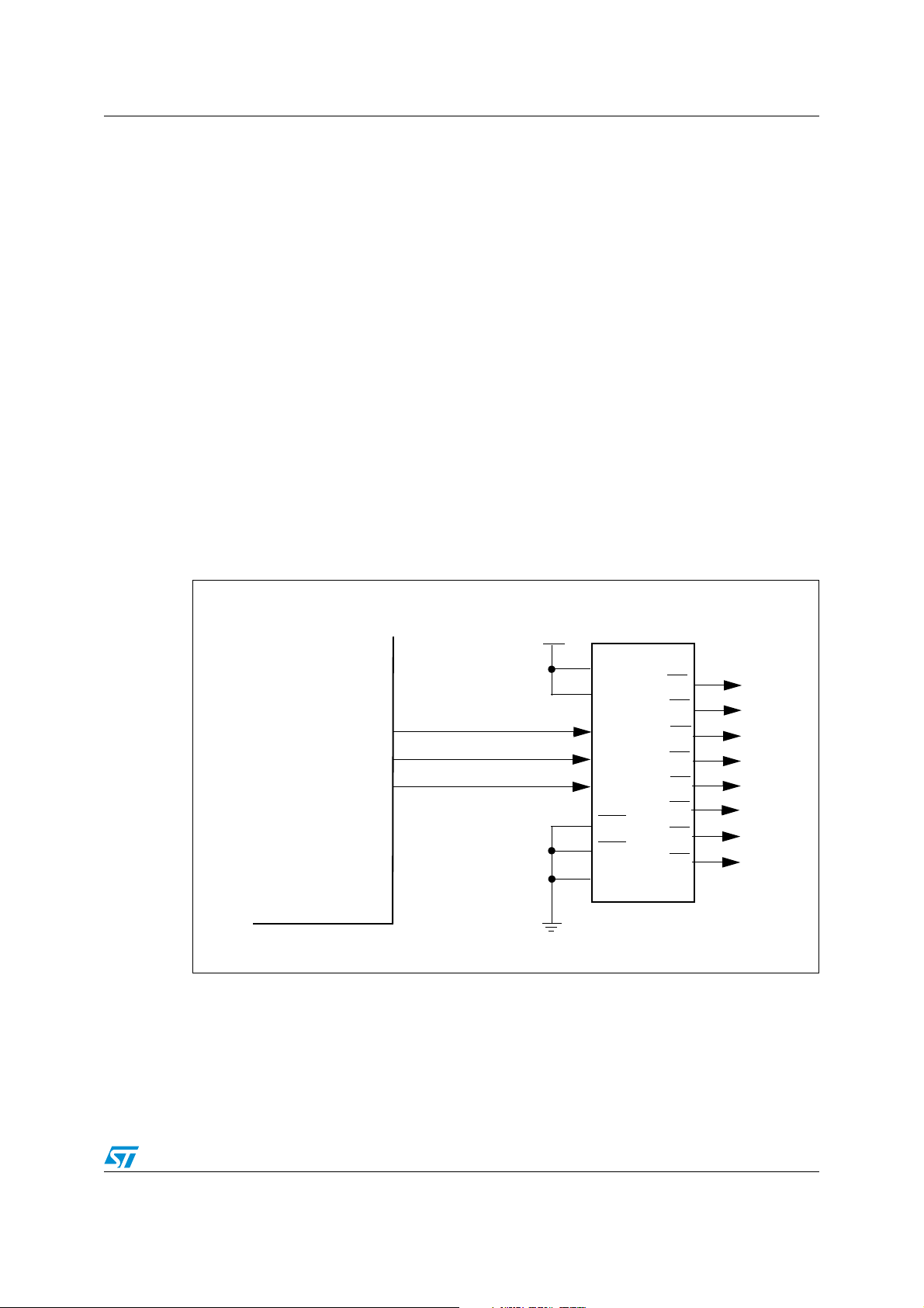
Figure 1 shows how to reduce the number of outputs used in this type of application.
This solution uses a 3-to-8 line decoder (M74HC138) to determine which one of the outputs
goes low (Y0 to Y7) by applying an address value on the three inputs A, B and C. The
number of lines saved is 8 - 3 = 5 lines.
Figure 1. Expander for 8 outputs using a M74HC138 decoder
16
6
1
2
3
4
5
8
M74HC138
Vcc
G1
A
B
C
G2A
G2B
GND
3.3v
µC
GPIO0.0
GPIO0.1
GPIO0.2
Y0
Y1
Y2
Y3
Y4
Y5
Y6
Y7
15
14
13
12
11
10
9
8
1.1.2 Expanding the number of outputs to 16 lines
Sometimes, more than 8 outputs are used although only one output needs to be active at a
time (for example for a multiplexed display with more than 8 digits, a matrix keypad with
more than 7 rows or a row of 16 LEDs for a bargraph level display, and so on).
3/19
Page 4
Expanding the number of outputs AN2591
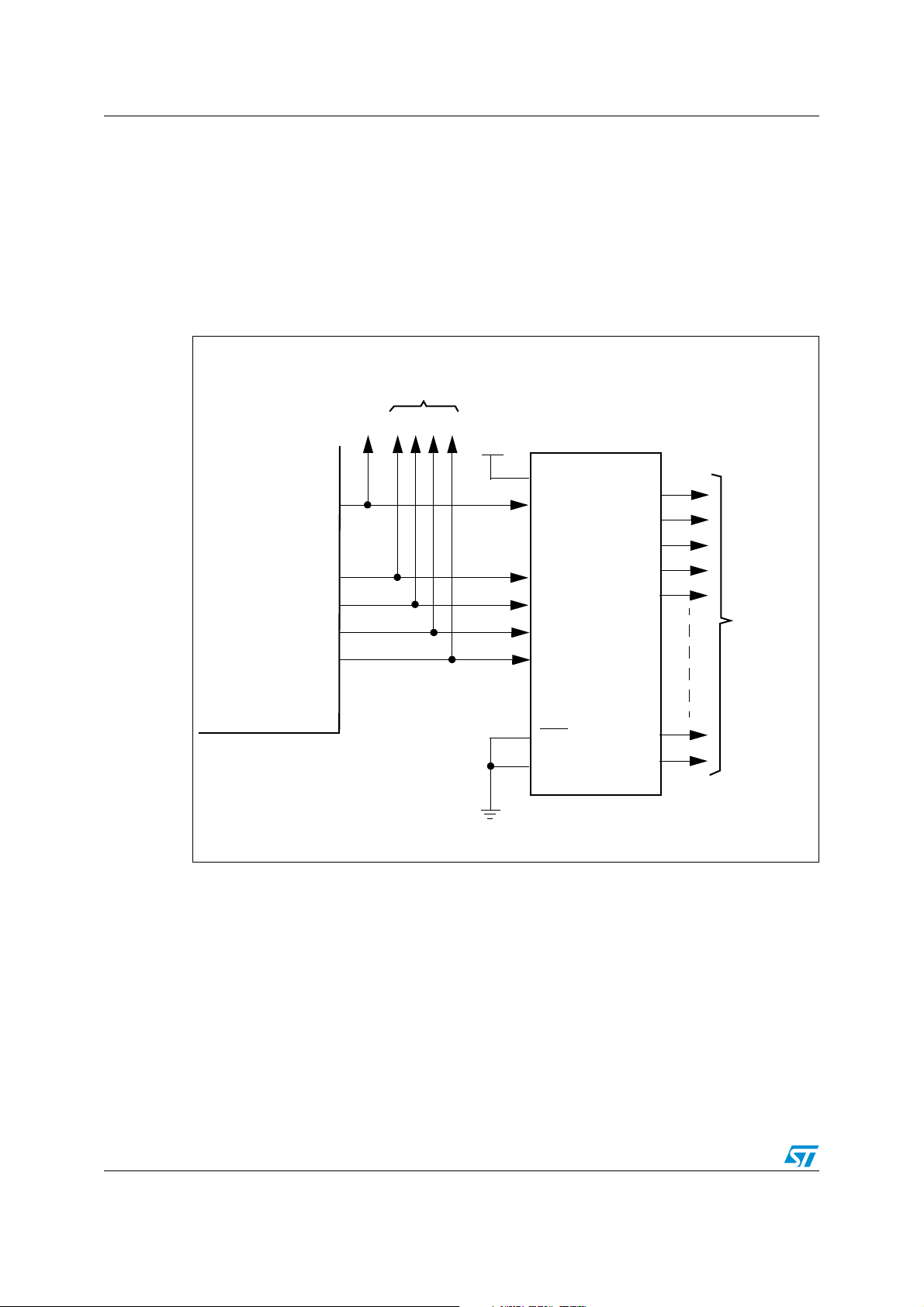
This example uses a 4-to-16 line decoder (M74HC4514 or M74HC4515) to expand the
number of outputs to 16. The number of lines saved is 16 - 5 = 11 lines.
Contrary to the solution described in Section 1.1.1, the microcontroller GPIOs connected to
the decoder address lines can also be used for other application purposes. This is made
possible by the decoder strobe input which stores the address of the decoder output. The
decoder output values remain unchanged while ST = 0, so in this state you can change the
GPIO values and you are free to use the lines (GPIO0.0 to GPIO0.3) for other application
purposes. In this case, the number of lines saved is 16 - 1 (for strobe line) = 15 lines.
Figure 2. Expander for 16 outputs using a M74HC4514 or M74HC4515 decoder
Can also be used for
other application purposes
µC
GPIO0.4
GPIO0.0
GPIO0.1
GPIO0.2
GPIO0.3
Strobe
3.3v
2
3
21
22
1
23
12
24
Vcc
A
B
C
INH
GND
M74HC4514 /
M74HC4515
ST
D
Y0
Y1
Y2
Y3
Y4
Y14
Y15
11
9
10
8
7
16 outputs
16
15
Note: M74HC4514 and M74HC4515 are similar and pin to pin compatible except that the latter
has inverted outputs.
1.2 Using a shift register
1.2.1 Expanding the number of outputs to 8 lines
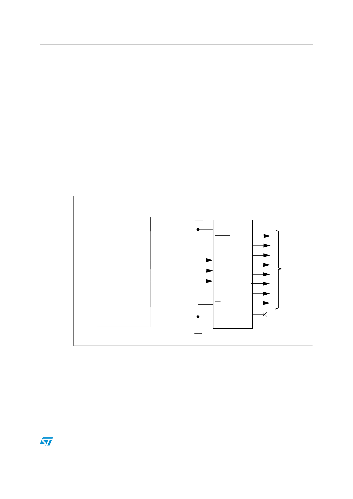
This is another technique you can use to free up some microcontroller lines. This example
uses a 74HC595 SIPO (Serial In / Parallel Out) shift register that requires only 3
microcontroller GPIOs to generate one byte of data on its outputs (Q0 to Q7) (see
M74HC595 datasheet).
4/19
Page 5
AN2591 Expanding the number of outputs
The shift register receives data serially from the microcontroller via the Sin input (pin 14)
using synchronous transmission. The M74HC595 includes two registers. The first one is a
shift register to shift in the data, the second one is a latch register to enable the data on the
outputs. This register prevents the output values being disturbed while data is being shifted
into the shift register.
You need to perform two steps to make the data available on the M74HC595 outputs:
1. Shift the data from the microcontroller to the shift register via the Sin line:
– Shift each bit of data via the microcontroller (GPIO0.0) and
– Apply a clock pulse (via SCK line) to shift this bit into the register. You need 8 clock
times to load all bits of the data byte into the shift register. At this stage the data is
not yet available on the outputs (Q0 to Q7).
2. To make it available on the outputs (Q0 to Q7), you must apply a latch pulse via the
RCK line to load the data into the second register.
The number of lines saved is 8 - 3 = 5. This is same amount of saving as with the
M74HC138 decoder but the difference that you can activate or deactivate any of the outputs
independently, unlike with the decoder when only one output can be activated at a time.
Figure 3. Expander for 8 outputs using a shift register: M74HC595
16
10
13
8
M74HC595
Vcc
SCLR
Sin
RCK
SCK
G
GND
µC
GPIO0.0
GPIO0.1
GPIO0.2
3.3v
14
12
11
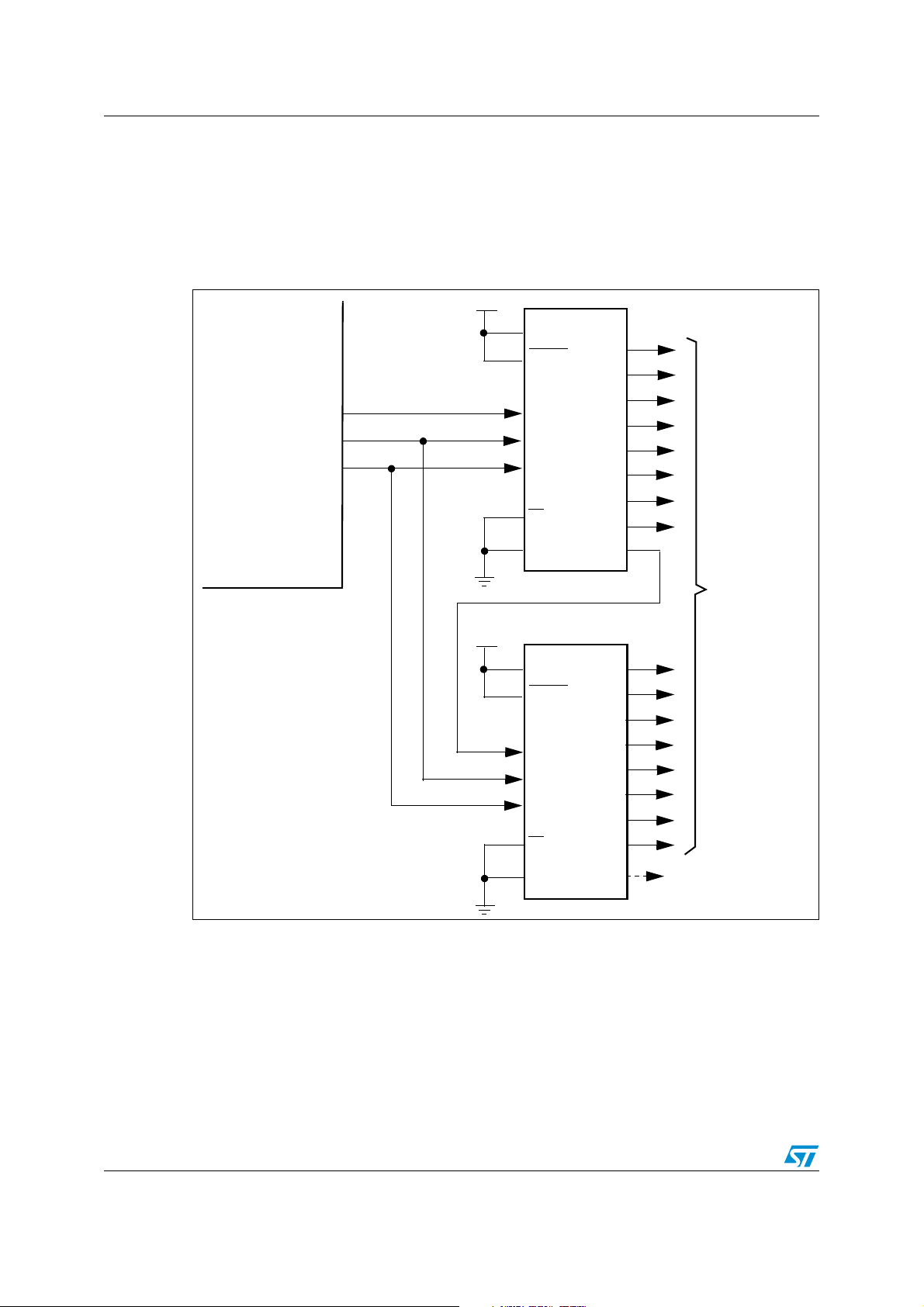
1.2.2 Expanding the number of outputs to 16 lines
In this section uses the same technique as described in Section 1.2.1, but the number of
outputs is expanded to 16 lines. This is done by cascading two shift registers (the same IC
reference used in Section 1.2.1).
Q0
Q1
Q2
Q3
Q4
Q5
Q6
Q7
SDO
15
1
2
3
4
5
6
7
9
8 outputs
The M74HC595 SDO output is used to connect the two shift registers to allow the data flow
to pass from the first register into the second one. This creates a 16-bit shift register.
5/19
Page 6
Expanding the number of outputs AN2591
The availability of data on the outputs of the two M74HC595 components is controlled by the
same sequence described in Section 1.2.1 but to make 16 bits of data, the process is done
for 16 clock times. You have to apply the latch pulse to the two ICs at the same time to
enable the data in the 16 output lines. You can expand the number of outputs even further
without using any additional microcontroller GPIO lines because there are two common
signals for all registers (RCK and SCK). The number of lines saved is 16 - 3 = 13.
Figure 4. Expander for 16 outputs using two shift registers: M74HC595
16
10
13
8
M74HC595
Vcc
SCLR
Sin
RCK
SCK
G
GND
Q0
Q1
Q2
Q3
Q4
Q5
Q6
Q7
SDO
15
1
2
3
4
5
6
7
9
µC
GPIO0.0
GPIO0.1
GPIO0.2
3.3v
14
12
11
3.3v
14
12
11
16
10
13
8
M74HC595
Vcc
SCLR
Sin
RCK
SCK
G
GND
Q0
Q1
Q2
Q3
Q4
Q5
Q6
Q7
SDO
15
1
2
3
4
5
6
7
9
To other registers if
needed to expand to
more than 16 outputs
16 outputs
6/19
Page 7

AN2591 Expanding the number of inputs
2 Expanding the number of inputs
To expand the number input lines, for example to get the state of several bi-state sensors or
to scan switch states, two techniques can be used: using multiplexers or shift registers.
2.1 Using a multiplexer
2.1.1 Expanding the number of inputs to 8 lines
Figure 5 shows an example of how a multiplexer can be connected to the microcontroller. To
get a bit value from a multiplexer input, apply the address value of the input via address lines
(A, B and C) and read it in via the multiplexer OUT output (pin 5). To get all 8 bits of data
available on the inputs (D0 to D7), you must read all bit states sequentially from the MSB
(address value = 0x7) to LSB (address value = 0x0) by decrementing the bit address and
applying it on GPIO0.0 to GPIO0.2. For each bit address you read the bit value and shift it
into the microcontroller on GPIO0.3 by software to build a data byte. The multiplexer used is
the M74HC151. This allows you to save 8 - 4 = 4 lines.
Figure 5. Expander for 8 inputs using a multiplexer: M74HC151
µC
GPIO0.0
GPIO0.1
GPIO0.2
GPIO0.3
3.3V
11
10
9
5
16
7
8
M74HC151
Vcc
A
B
C
Out
ST
GND
D0
D1
D2
D3
D4
D5
D6
D7
4
3
2
1
15
14
13
12
8 inputs
7/19
Page 8

Expanding the number of inputs AN2591
2.1.2 Expanding the number of inputs to 16 lines
This section uses the same technique as described in Section 2.1.1.
The M74HC4067 multiplexer 16 to 1 is used to expand the input lines to 16. In this case the
number of lines saved is 16 - 5 = 11.
To get 16 bits of data from the multiplexer inputs you must scan all inputs (as described in
Section 2.1.1) by applying a 4 bit address to the A,B,C and D lines sequentially from MSB
(address value = 0xF) to LSB (address value = 0x0) and shift each bit into the
microcontroller to build a 16 bit data word.
Figure 6. Expander for 16 inputs using a multiplexer: M74HC4067
µC
GPIO0.0
GPIO0.1
GPIO0.2
GPIO0.3
GPIO0.4
3.3v
10
11
14
13
1
M74HC4067
24
Vcc
A
B
C
D
Out
15
E
12
GND
Y0
Y1
Y2
Y3
Y4
Y5
Y6
Y7
Y8
Y9
Y10
Y11
Y12
Y13
Y14
Y15
9
8
7
6
5
4
3
2
23
22
21
20
19
18
17
16
16 inputs
8/19
Page 9

AN2591 Expanding the number of inputs
2.2 Using shift registers
2.2.1 Expanding the number of inputs to 8 lines
A PISO (Parallel In Serial Out) shift register can also be used to increase the number of
inputs. Figure 7 shows how to connect a shift register M74HC165 to a microcontroller using
only 3 GPIOs.
The shift register sends data serially to the microcontroller via its QH output (pin 9) using
synchronous communication.
First, you load the 8 bit data available on the inputs (A to H) into the register by applying a
load pulse (set it low and then high again), the 8 bits of data are loaded in parallel into the
register. The logic level that was present at the H input appears immediately on the QH
output when the latch pulse is applied. Then, on each subsequent rising edge of the clock
(pin 2), the logic level of the next bit appears on the QH output and can be read via the
GPIO0.2 input and shifted by software to build a byte of data. 8 bits of data take 7 clock
pulses (generated by the microcontroller) to shift out one byte and not 8 clocks because
initially the higher bit was present on QH.
The number of lines saved is 8 - 3 = 5.
Figure 7. Expander for 8 inputs using a shift register: M74HC165
µC
GPIO0.0
GPIO0.1
GPIO0.2
3.3v
16
1
2
9
15
10
8
M74HC165
Vcc
S/L
CK
QH
QH
CK INH
SI
GND
11
A
12
B
13
C
14
D
E
F
H
3
4
5
G
6
8 inputs
9/19
Page 10

Expanding the number of inputs AN2591
2.2.2 Expanding the number of inputs to 16 lines
To expand the number of inputs to more than 8 using shift registers, you can cascade two or
more shift registers by connecting the QH output of one shift register, that receives the
inputs for the low order
for the high order
have its QH output directly connected to the microcontroller. The same technique as
described in Section 2.2.1 is used to read all 16 inputs and 15 clock pulses generated by the
microcontroller to get all 16 bits of data.
In this case, when two registers are used, the number of lines saved is 16 - 3 = 13.
By cascading more than two registers, in order to expand more than 16 inputs, the number
of GPIOs used for this technique remains the same: always 3 lines from the microcontroller.
Figure 8. Expander for 16 inputs using two shift registers: 74HC165
data byte, to the SI input of the next register that receives the inputs
data byte. The register for the high order data byte is the one that must
µC
GPIO0.0
GPIO0.1
GPIO0.2
From previous register
QH output if needed to
expand more than 16 inputs
if not used it must be tied
to ground
3.3v
10
3.3v
16
1
2
9
7
15
8
16
9
7
1
2
15
10
8
M74HC165
Vcc
S/L
CK
QH
QH
SI
CK INH
GND
M74HC165
Vcc
QH
QH
S/L
CK
CK INH
SI
GND
A
B
C
D
E
F
G
H
A
B
C
D
E
F
G
H
11
12
13
14
3
4
5
6
11
12
13
14
3
4
5
6
I8
I9
I10
I11
I12
I13
I14
I15
16 inputs
I0
I1
I2
I3
I4
I5
I6
I7
10/19
Page 11

AN2591 Using a STMPE801 (I²C bus) 8-bit I/O port expander
3 Using a STMPE801 (I²C bus) 8-bit I/O port expander
The STMPE801 is a General Purpose Input / Output (GPIO) expander specially designed
for expanding the input/output lines and solving the common problem of not having enough
GPIOs available for the application. This IC offers several features:
● 8 available GPIOs.
● Each GPIO can be individually configured as input or output in the data direction
register GPDR and can be a source of an external interrupt configurable in the
IEGPIOR register.
● This device interfaces to the microcontroller using an I
● Up to 2 devices (2 x STMPE801) can share the same I
Note: For more details refer to the STMPE801 datasheet.
3.1 Expanding the number of inputs/outputs to 8 lines
2
C bus.
2
C bus.
Figure 9 shows how the STMPE801 is connected via I2C bus to the microcontroller. When
ADDR0 pin is connected to ground, the I
2
C device address will be 0x82, otherwise (ADDR0
= Vcc) the device address will be 0x88.
Figure 9. Eight channel expander
STMPE801MTR
16
VCC
1
VIO
SDAT
SCLK
11
INT
RESET
14
ADDR0
2
GND
GPIO0
GPIO1
GPIO2
GPIO3
GPIO4
GPIO5
GPIO6
GPIO7
3
4
5
6
7
8
10
8 inputs/
outputs
9
µC
GPIOX.Y
SDA
SCL
XTI
3.3v
R1 R2
4.7K 4.7K
15
13
If needed
12
(I2C device address=0x82)
Each GPIO (0 to 7) can be configured independently as input or output (see details in the
GPDR section in STMPE801 datasheet). You can read the state of each GPIO in the GPMR
register. To set a GPIO state, you need to set its value in the GPSR register.
The INT (interrupt) output can be optionally used to increase the number of external interrupt sources of the microcontroller by connecting it to one of external interrupt lines: XTI
microcontroller interrupt input. To use this option, you must first configure the IEGPIOR register to enable the interrupt from a particular GPIO interrupt source to the host. After that,
11/19
Page 12

Using a STMPE801 (I²C bus) 8-bit I/O port expander AN2591
you must configure the INTPolarity bit and the INT_Enable bit in the SystemControl register
(address = 0x04).
You must read the ISGPIOR register in interrupt routine to determine which GPIO has
generated the interrupt. Each bit of this register, represents the interrupt status of each
GPIO pin.
The VIO pin is provided to fix the voltage used by the GPIOs. The VIO pin level, must be
greater than or equal to the Vcc level.
The RESET input pin is connected to any microcontroller GPIO to initialize the STMPE801
when it is needed.
3.2 Expanding the number of I/Os to 16 lines
The STMPE801 design supports connecting up to two devices in the same I2C bus to obtain
16 additional input/output lines.
Figure 10 shows how two STMPE801 share the two lines of the I2C interface with different
addresses. The first device the has its ADDR0 input connected to ground will have the
address 0x82, whereas the ADDR0 input of the second device is connected to Vcc to fix the
I2C device address to 0x88.
It is possible to use the two interrupt outputs of the two devices to expand the interrupt lines
to 16. Each interrupt output (INT: pin 11) is connected to an interrupt input (two interrupt
inputs are used, see Figure 10).
Note: When only one interrupt is available in the microcontroller you are using, you can add an
appropriate logic gate to connect the two INT outputs to its inputs and connect the gate
output to the interrupt input of the microcontroller. In this case, to determine which GPIO has
generated the interrupt, you must read the ISGPIOR register of each device).
12/19
Page 13

AN2591 Using a STMPE801 (I²C bus) 8-bit I/O port expander
Figure 10. 16-channel expander
STR710
GPIOX.Y
SDA
SCL
XTI0
XTI1
R1 R2
4.7K 4.7K
If needed
If needed
3.3v
STMPE801MTR
16
VCC
1
VIO
GPIO0
GPIO1
15
13
12
11
14
2
SDAT
SCLK
INT
RESET
ADDR0
GND
GPIO2
GPIO3
GPIO4
GPIO5
GPIO6
GPIO7
(I2C device address=0x82)
3.3V
STMPE801MTR
16
VCC
1
VIO
14
ADDR0
15
13
12
11
2
SDAT
SCLK
RESET
INT
GND
GPIO0
GPIO1
GPIO2
GPIO3
GPIO4
GPIO5
GPIO6
GPIO7
3
4
5
6
7
8
9
10
16 inputs/
outputs
3
4
5
6
7
8
9
10
(I2C device address=0x88)
13/19
Page 14

Using the External Memory Interface for I/O expansion AN2591
4 Using the External Memory Interface for I/O
expansion
The EMI can be used not only to interface external memories, but also to create additional
microcontroller ports.
lines when all GPIOs are used and you need more GPIOs. In this section we give a solution
using latches and buffers that allows you to expand the number of inputs and/or outputs
using the EMI interface of the STR710 microcontroller.
4.1 Expanding the number of inputs and/or outputs to 8 lines
Figure 11 shows how the input/output expander is implemented using 74LCX573 (8-bit
latch) to create an 8-line output port and 74LCX244 (8-bit buffer) to create an 8-line input
port (see 74LCX573 and 74LCX244 datasheets). The latch inputs and the buffer outputs are
connected to the LSB data byte: D0 to D7.
Figure 11. Eight-channel expander
STR710
D[0..15]
The EMI can be used to expand the number of inputs and/or outputs
EMI
data bus
16
16
8
D[0..7]
11
1
74LCX573
D[0..7]
LE
OE
VDD
Q[0..7]
GND
3.3v
20
8
8 outputs
10
RD
74V1G02
74V1G08
8
WRL
CSn.x
To put a byte of data on the latch outputs, you must write the data in an address located in
address range corresponding to the CSn.x bank. For example, if the CSn.x used is CSn.0,
and the EMI address is not remapped at address 0 (EMI address range = 0x60000000 to
14/19
19
D[0..7]
1
74LCX244
1G
2G
1Y-2Y
VDD
1A-2A
GND
3.3v
20
8
8 inputs
10
Page 15

AN2591 Using the External Memory Interface for I/O expansion
0x6C00000C), the bank0 address range will be 0x60000000 to 0x60FFFFFF. So the register
and the buffer addresses must be included in this range for example:
Register address: 0x60000001.
Buffer address: 0x60000002.
Note: You can use the same address for the register and the buffer.
The bank used for the buffer and the register is reserved only for these devices and does not
use any memory or other device in this bank.
EMI configuration:
● Configure the EMI effective external bus size as 8-bit data bus wide to read from the
external 8-bit buffer and to write in the external 8-bit register.
● Configure the number of wait states to obtain a WRL pulse width delay greater than
15ns (15ns is the greatest propagation time value of the latch, buffer, NOR and AND
gates. Refer to the 74LCX573, 74LCX244, 74V1G02 and 74V1G08 datasheets).
Note: The WRL and RD pulse widths must be greater than the propagation delay of the circuit
which has the highest propagation delay (in this case 74V1G08, refer to its datasheet). So
you must configure the corresponding number of wait states to write to the register and to
read from the buffer properly.
Example of software that gets the value of the 8-bit buffer inputs and writes it in the 8-bit
latch outputs. The two devices are available in bank0 (CSn.x = CSn.0):
int main(void)
{
u8 a;
u8 *Buffer_Data8_in = (u8*)0x60000002; /* Initialize the buffer
address to 0x60000002 */
u8 *Latch_Data8_out = (u8*)0x60000001; /* Initialize the latch
address to 0x60000001 */
*(u8*)0x6C000000 = 0x8004; /* Configure EMI_BCON0 register:
- 8 bit data bus wide
- 1 wait state
- Enable bank 0 */
while(1)
{
a = *Buffer_Data8_in; /* Get the value available on inputs of
the external buffer */
*Latch_Data8_out = a; /* Write this value in the external
latch */
}
}
15/19
Page 16

Using the External Memory Interface for I/O expansion AN2591
4.2 Expanding the number of inputs and/or outputs to 16 lines
In this section, the same hardware structure is implemented as described in Section 4.1,
except that a 16-bit latch (74LCX16373) and 16-bit buffer (74LCX16244) are used.
It is important to know the propagation delay times of the devices you are using in order to
configure the corresponding number of wait states (Refer to the 74LCX16373,
74LCX16244, 74V1G02 and 74V1G08 datasheets).
Figure 12. 16-channel expander
EMI
data bus
16
D[0..15]
74LCX16373
1D-2D[0..16]
VDD*
3.3v
16
16 outputs
3.3v
16
16 inputs
25
24
48
48
25
24
D[0..15]
1
1LE
2LE
1OE
2OE
74LCX16244
1
1G
2G
3G
4G
1Y-2Y-3Y-4Y
1Q-2Q[0..16]
GND*
VDD*
1A-2A-3A-4A
GND*
16
STR710
16
D[0..15]
74V1G02
WRL
CSn.x
RD
74V1G08
16
Note (*): The VDD and GND power inputs of 74LCX16373 and 74LCX16244 are not all
represented in this figure: VDD pins of the two devices are: 7, 18, 31 and 42, must connected to
3.3V.
All GND pins of the two devices are: 4, 10, 15, 21, 28, 34, 39 and 45, must connected to ground.
For more details refer to the IC datasheets.
16/19
Page 17

AN2591 Using the External Memory Interface for I/O expansion
Example of software that gets the value on the 16-bit buffer inputs and writes it in the 16-bit
latch outputs. The two devices are available in bank0 (CSn.x = CSn.0):
int main(void)
{
u16 a;
u16 *Buffer_Data16_in = (u16*)0x60000002; /* Initialize the buffer
address to 0x60000002 */
u16 *Latch_Data16_out = (u16*)0x60000001; /* Initialize the latch
address to 0x60000001 */
*(u16*)0x6C000000 = 0x8005; /* Configure EMI_BCON0 register:
- 16 bit data bus wide
- 1 wait state
- Enable bank 0 */
while(1)
{
a = *Buffer_Data16_in; /* Get the value available on inputs
of the external buffer */
*Latch_Data16_out = a; /* Write this value in the external
latch */
}
}
17/19
Page 18

Revision history AN2591
5 Revision history
Table 1. Document revision history
Date Revision Changes
06-Aug-2007 1 Initial release.
18/19
Page 19

AN2591
Please Read Carefully:
Information in this document is provided solely in connection with ST products. STMicroelectronics NV and its subsidiaries (“ST”) reserve the
right to make changes, corrections, modifications or improvements, to this document, and the products and services described herein at any
time, without notice.
All ST products are sold pursuant to ST’s terms and conditions of sale.
Purchasers are solely responsible for the choice, selection and use of the ST products and services described herein, and ST assumes no
liability whatsoever relating to the choice, selection or use of the ST products and services described herein.
No license, express or implied, by estoppel or otherwise, to any intellectual property rights is granted under this document. If any part of this
document refers to any third party products or services it shall not be deemed a license grant by ST for the use of such third party products
or services, or any intellectual property contained therein or considered as a warranty covering the use in any manner whatsoever of such
third party products or services or any intellectual property contained therein.
UNLESS OTHERWISE SET FORTH IN ST’S TERMS AND CONDITIONS OF SALE ST DISCLAIMS ANY EXPRESS OR IMPLIED
WARRANTY WITH RESPECT TO THE USE AND/OR SALE OF ST PRODUCTS INCLUDING WITHOUT LIMITATION IMPLIED
WARRANTIES OF MERCHANTABILITY, FITNESS FOR A PARTICULAR PURPOSE (AND THEIR EQUIVALENTS UNDER THE LAWS
OF ANY JURISDICTION), OR INFRINGEMENT OF ANY PATENT, COPYRIGHT OR OTHER INTELLECTUAL PROPERTY RIGHT.
UNLESS EXPRESSLY APPROVED IN WRITING BY AN AUTHORIZED ST REPRESENTATIVE, ST PRODUCTS ARE NOT
RECOMMENDED, AUTHORIZED OR WARRANTED FOR USE IN MILITARY, AIR CRAFT, SPACE, LIFE SAVING, OR LIFE SUSTAINING
APPLICATIONS, NOR IN PRODUCTS OR SYSTEMS WHERE FAILURE OR MALFUNCTION MAY RESULT IN PERSONAL INJURY,
DEATH, OR SEVERE PROPERTY OR ENVIRONMENTAL DAMAGE. ST PRODUCTS WHICH ARE NOT SPECIFIED AS "AUTOMOTIVE
GRADE" MAY ONLY BE USED IN AUTOMOTIVE APPLICATIONS AT USER’S OWN RISK.
Resale of ST products with provisions different from the statements and/or technical features set forth in this document shall immediately void
any warranty granted by ST for the ST product or service described herein and shall not create or extend in any manner whatsoever, any
liability of ST.
ST and the ST logo are trademarks or registered trademarks of ST in various countries.
Information in this document supersedes and replaces all information previously supplied.
The ST logo is a registered trademark of STMicroelectronics. All other names are the property of their respective owners.
© 2007 STMicroelectronics - All rights reserved
STMicroelectronics group of companies
Australia - Belgium - Brazil - Canada - China - Czech Republic - Finland - France - Germany - Hong Kong - India - Israel - Italy - Japan -
Malaysia - Malta - Morocco - Singapore - Spain - Sweden - Switzerland - United Kingdom - United States of America
www.st.com
19/19
 Loading...