

Page 1
AN2590
Application note
20 W dimmable CFL ballast solution
Introduction
This application note describes the 20 W dimmable CFL ballast solution which can
completely replace incandescent lamps in formal dimming systems. The dimmer controlled
range is 20% - 100% of full light output without changing the formal triac dimmer.
Compared to the formal CFL solution, this solution not only provides energy savings, but
also higher reliability and a much longer operating life.
The solution is based on the high performance ballast driver L6574D, two of the
STD4NK50Z Zener protected SuperMESH™ Power MOSFETs, and two of the STTH1L06
turbo 2 ultra fast high voltage rectifiers.
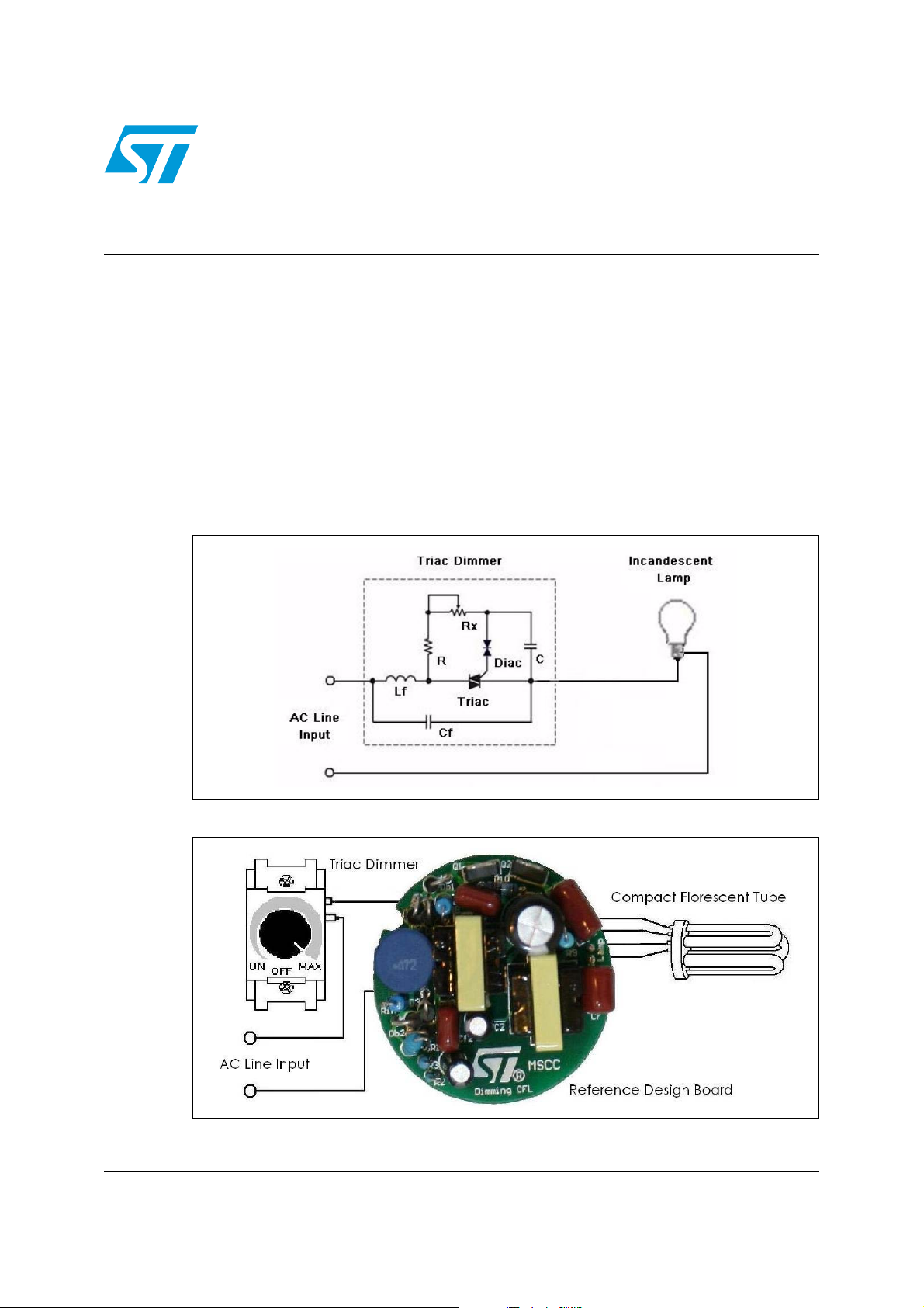
Figure 1. Typical dimmer
Figure 2. Dimming CFL ballast solution
October 2007 Rev 1 1/17
www.st.com
Page 2

Contents AN2590
Contents
1 Typical dimming system for incandescent lamps . . . . . . . . . . . . . . . . . 4
1.1 Formal CFL ballast and its disadvantages . . . . . . . . . . . . . . . . . . . . . . . . . 4
1.2 Proposed solution . . . . . . . . . . . . . . . . . . . . . . . . . . . . . . . . . . . . . . . . . . . . 5
2 Board description . . . . . . . . . . . . . . . . . . . . . . . . . . . . . . . . . . . . . . . . . . . 6
2.1 Application circuit . . . . . . . . . . . . . . . . . . . . . . . . . . . . . . . . . . . . . . . . . . . . 6
2.2 Dimming function . . . . . . . . . . . . . . . . . . . . . . . . . . . . . . . . . . . . . . . . . . . . 7
2.3 Principle of the main circuit . . . . . . . . . . . . . . . . . . . . . . . . . . . . . . . . . . . . 7
2.4 Calculations . . . . . . . . . . . . . . . . . . . . . . . . . . . . . . . . . . . . . . . . . . . . . . . . 8
3 Electrical specifications and reference design board . . . . . . . . . . . . . 10
3.1 Electrical specifications . . . . . . . . . . . . . . . . . . . . . . . . . . . . . . . . . . . . . . 10
3.2 PCB layout view . . . . . . . . . . . . . . . . . . . . . . . . . . . . . . . . . . . . . . . . . . . . 10
4 Test results . . . . . . . . . . . . . . . . . . . . . . . . . . . . . . . . . . . . . . . . . . . . . . . 11
5 Conclusion . . . . . . . . . . . . . . . . . . . . . . . . . . . . . . . . . . . . . . . . . . . . . . . . 14
5.1 References . . . . . . . . . . . . . . . . . . . . . . . . . . . . . . . . . . . . . . . . . . . . . . . . 14
6 Revision history . . . . . . . . . . . . . . . . . . . . . . . . . . . . . . . . . . . . . . . . . . . 16
2/17
Page 3

AN2590 List of figures
List of figures
Figure 1. Typical dimmer . . . . . . . . . . . . . . . . . . . . . . . . . . . . . . . . . . . . . . . . . . . . . . . . . . . . . . . . . . . 1
Figure 2. Dimming CFL ballast solution . . . . . . . . . . . . . . . . . . . . . . . . . . . . . . . . . . . . . . . . . . . . . . . . 1
Figure 3. Typical dimming system consisting of incandescent lamp and triac dimmer . . . . . . . . . . . . 4
Figure 4. Block diagram of formal CFL ballast. . . . . . . . . . . . . . . . . . . . . . . . . . . . . . . . . . . . . . . . . . . 4
Figure 5. The half AC line cycle of sinuous wave and firing angle. . . . . . . . . . . . . . . . . . . . . . . . . . . . 5
Figure 6. Schematic of the reference design board . . . . . . . . . . . . . . . . . . . . . . . . . . . . . . . . . . . . . . . 6
Figure 7. Main circuit . . . . . . . . . . . . . . . . . . . . . . . . . . . . . . . . . . . . . . . . . . . . . . . . . . . . . . . . . . . . . . 7
Figure 8. L1 current per switching period. . . . . . . . . . . . . . . . . . . . . . . . . . . . . . . . . . . . . . . . . . . . . . . 8
Figure 9. L1 current shape . . . . . . . . . . . . . . . . . . . . . . . . . . . . . . . . . . . . . . . . . . . . . . . . . . . . . . . . . . 8
Figure 10. PCB top-side view . . . . . . . . . . . . . . . . . . . . . . . . . . . . . . . . . . . . . . . . . . . . . . . . . . . . . . . 10
Figure 11. PCB bottom-side view . . . . . . . . . . . . . . . . . . . . . . . . . . . . . . . . . . . . . . . . . . . . . . . . . . . . 10
Figure 12. Full load efficiency vs. AC line input . . . . . . . . . . . . . . . . . . . . . . . . . . . . . . . . . . . . . . . . . . 11
Figure 13. Triac turn-on time vs. power dissipation to the lamp. . . . . . . . . . . . . . . . . . . . . . . . . . . . . . 11
Figure 14. AC input voltage and current . . . . . . . . . . . . . . . . . . . . . . . . . . . . . . . . . . . . . . . . . . . . . . . 12
Figure 15. L1 voltage and current . . . . . . . . . . . . . . . . . . . . . . . . . . . . . . . . . . . . . . . . . . . . . . . . . . . . 12
Figure 16. Power factor in operating range . . . . . . . . . . . . . . . . . . . . . . . . . . . . . . . . . . . . . . . . . . . . . 12
Figure 17. Lamp voltage and current at Ton=9 ms, Vlamp=100 V/div, Ilamp= 200 mA/div. . . . . . . . . 13
Figure 18. Lamp voltage and current at Ton=5 ms, Vlamp=100 V/div, Ilamp= 200 mA/div. . . . . . . . . 13
Figure 19. Lamp voltage and current at Ton=3 ms, Vlamp=100 V/div, Ilamp= 200 mA/div. . . . . . . . . 13
3/17
Page 4
Typical dimming system for incandescent lamps AN2590
1 Typical dimming system for incandescent lamps
A typical dimming system consists of the lamp(s) and dimmer (Figure 3). The dimmer
consists of the triac and a few components, see Figure 1. Dimmers of this type are
appropriate for incandescent lamps and are very popular in the market.
Figure 3. Typical dimming system consisting of incandescent lamp and triac
dimmer
The triac conducts once it has been triggered and holds latching current. The triac shuts
down when the current is less than the holding current. The dimmer works fine with a
resistive load. The triac can be triggered at any timing of the sinuous voltage (AC line input),
and can be kept in conduction state until reaching zero line voltage. This allows the lamp to
be dimmed nearly to 100%.
1.1 Formal CFL ballast and its disadvantages
Since the formal CFL is not a resistive load, the ballast has no power factor correction circuit
(PFC). If the incandescent lamp (Tungsten filament light bulb) is replaced by a formal CFL
(Compact Florescent Lamp) directly, the CFL cannot fully illuminate and may have
intermittant blinking or no light at all. Figure 4 shows the block diagram of a formal CFL.
Figure 4. Block diagram of formal CFL ballast
The formal CFL ballast consists of a rectifier, storage capacitor, ballast driver circuit, half
bridge and resonant circuit. The source energy stored only to the storage capacitor from the
AC input at the timing nears its peak voltage per half cycle. When the formal CFL ballast is
connected to the triac dimmer (see Figure 1), the triac conducts only after having been
triggered, that is, when the rectified voltage is higher than the voltage across the storage
capacitor. At this extreme moment the capacitor can be charged with the same peak from
4/17
Page 5
AN2590 Typical dimming system for incandescent lamps
the AC input, and the triac is then immediately turned off. It is impossible to adjust the DC
voltage across the storage capacitor and then extend triac firing angle less than 90°.
However the lamp may continue to flicker and remain unstable if the DC voltage is not well
managed.
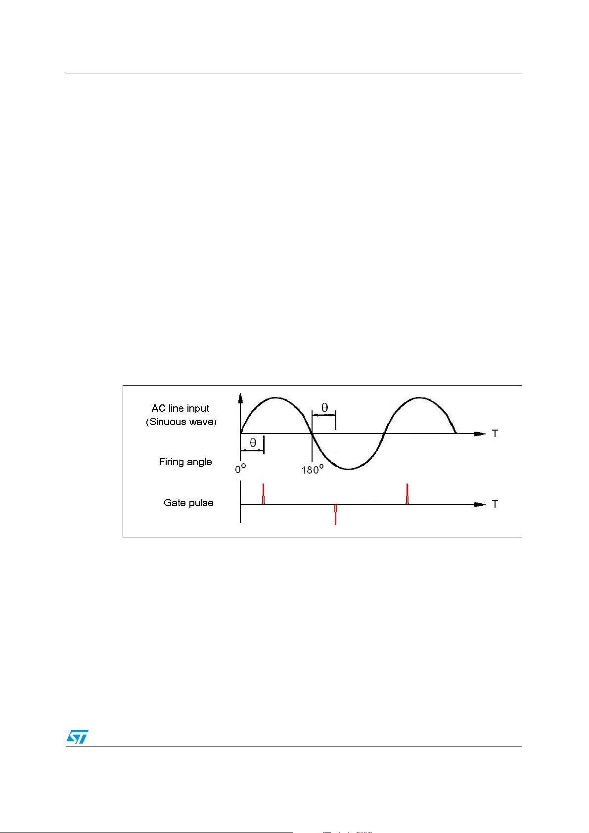
1.2 Proposed solution
The CFL ballast has been developed based on the L6574D. The lamp power can be
dimmed from below 20% up to 100% (full illumination) by adjusting the triac dimmer.
With the implementation of the PFC solution, the lamp power can be adjusted by switching
the frequency of the driver circuit that corresponds to the illumination level set by the triac
dimmer. The triac can be triggered at every point during the half cycle and conducts
continuously until the end of the half cycle (180°). In addition, a circuit detects the firing
angle of the triac and adjusts lamp power by adjusting the switching frequency of the half
bridge to control lamp power depending on the position of the triac dimmer.
Please note that while the triac dimmer is connected to the capacitive load (CFL), the triac
will not be fired if trigger angle is set lower than 50°. Because bus voltage (the voltage
across the storage capacitor) falls, the system stops operating at an angle less than 40°. For
this reason, the dimmable ballast cannot be operated in full dimming range. A hysteretic
range per half AC cycle was turned on at 50° and turned off at 40°. Figure 5 shows us the
Gate pulse (trigger) and firing angle per half cycle.
Figure 5. The half AC line cycle of sinuous wave and firing angle
5/17
Page 6
Board description AN2590
2 Board description
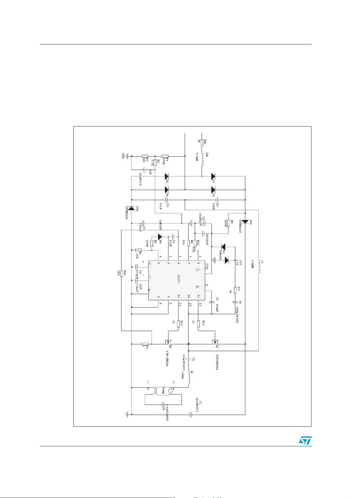
2.1 Application circuit
The reference design board is made according to the schematic shown in Figure 6. It
includes an LC filter, bridge rectifier, single stage PFC with high frequency ballast driver and
resonant circuit.
Figure 6. Schematic of the reference design board
RAFT
6/17
Page 7

AN2590 Board description
2.2 Dimming function
The two modes for dimming function are frequency modulation and voltage modulation.
In this solution, the dimming function is obtained using two methods: frequency modulation
and voltage modulation. When the trigger angle of the triac changes from 0° to 90°, only
frequency modulation works. When the angle changes from 90° to 180°, both of them work,
and voltage modulation dominates.
Frequency modulation depends on the operational amplifier in L6574D. In Figure 6, R1, R2,
R3 and C10 were used to simulate the trigger angle of the triac. When the angle changes
from 0° to 180°, the voltage across C10 which is the positive input of the amplifier (Pin 7,
here pin number is for L6574D), decreases accordingly. The output (Pin 5) of the amplifier
decreases with Pin 7, and the negative input (Pin 6) of the amplifier automatically
decreases. The equivalent resistance between Pin 4 and GND of the IC decreases, so the
switching frequency increases, hence lamp power decreases. If the angle changes from
180° to 360°, lamp power increases.
Voltage modulation means that the voltage across C1 (see Figure 6) decreases when the
firing angle of the triac changes from 90° to 180°. This makes the lamp power decrease.
2.3 Principle of the main circuit
In order to simplify the analysis, the main circuit is shown in Figure 7. There are two
independent circuits, power factor correction (PFC) circuit and half bridge resonant circuit.
The PFC which is labeled as A (dotted line) consists of Cf1, Cf2, L1, Db1, Db2, S1, S2 and
C1. The other one is a half bridge resonant circuit, which is labeled as B (solid line). It
consists of C1, S1, S2, Cb, Lr, Cr and the Lamp. S1 and S2, the Power MOSFETs operate
complementarily at almost 0.5 duty ratio.
Figure 7. Main circuit
Since the switching frequency was high enough, the voltages across the divider capacitors
(Cf1&Cf2) can be treated as constant during one switching cycle. Thus the voltage across
C1 is always higher than the line peak. In Figure 8 per switching cycle shows the model of a
four stage current flow through L1.
7/17
Page 8

Board description AN2590
● Stage 1: [t0... t1] charge to L1. At t0, S1 is already turned on and S2 is off. Assume the
current through L1 (iL1) is zero, then iL1 increases linearly by the voltage across Cf1,
and the current flows through Cf1, Db1, S1 and L1.
● Stage 2: [t1… t2] discharging by L1. At t1, S1 is turned off and S2 is turned on. At the
moment iL1 reaches the positive peak that forces Ds2 to turn on, negative voltage
(Vc1-Vcf1) is applied to L1, causing iL1 to decrease linearly. The current flows through
Cf1, Db1, C1, Ds2 and L1.
● Stage 3: [t2… t3] charge to L1. At t2, iL1 reaches zero, and iL1 linearly increases to the
negative peak by the voltage across Cf2. The current flows through Cf2, L1, S2 and
Db2.
● Stage 4: [t3… t4] discharging by L1. At t3, S1 is turned on and S2 is turned off. When
iL1 reaches the negative peak that forces Ds1 to turn on, voltage (Vc1-Vcf2) is applied
to L1, causing iL1 to decrease linearly. The current flows through Cf2, L1, Ds1, C1 and
Db2. At t4, iL1 reaches zero, where the new switching cycle begins.
Figure 8. L1 current per switching period Figure 9. L1 current shape
The overall current flow shape in L1 during one half AC line cycle is shown in Figure 9. It is
clear that the boost inductor current flows in two directions and the PFC circuit works at
boundary conduction mode.
2.4 Calculations
From the above analysis, the main parameters of the circuit can be calculated for the
application. To design the PFC circuit, the inductor (L1) and its peak current (Ipk) are the
most important.
For the resonant circuit, Lr and Cr are the main parameters. The calculation steps are given
as follows:
● Step 1: Ipk during one switching cycle is given by,
Equation 1
1
-- -
Vin
2
--------------------------------------------
Ipk
Where Vin is the input voltage after rectifier, Ts is the period of a switching time, t' is the
discharging time of L1, and Vc1 is the voltage across C1.
8/17
1
⎛⎞
-- -
Ts t'–
•
⎝⎠
2
L1
Vc1
-------------------------------------- -==
1
-- -
2
L1
Vin t'•–
Page 9

AN2590 Board description
As a consequence of that, we have the following.
Equation 2
Vin
--------------
t'
4Vc1
Ts=
Equation 3
Ipk
● Step 2: The input ac current (Iac) equals half of the average inductor current due to two
4L1
• Vin•=
Ts
----------
Vin
⎛⎞
1
--------------–
⎝⎠
2Vc1
divider capacitors, so,
Equation 4
1
⎛⎞
Iac
● Step 3: The input power Pin is determined by,
-- -
i
L1
⎝⎠
2
ave
1
-- -
4
Ipk
Ts
------------- -
16L 1
Vin
⎛⎞
1
--------------–
• Vin•===
⎝⎠
2Vc1
Equation 5
π
1
-- -
Pin
=
π
Vac Iac•θd
∫
0
Where Vac is the input voltage. With the above three steps, the values of L1 and Ipk can be
found if the input/output conditions and switching frequency are given.
● Step 4: For the half bridge resonant circuit, the equivalent resistance of the lamp is
given by:
Equation 6
V
rms lamp,
---------------------------=
I
rms lamp,
rms,lamp
is the rated lamp current. With V
rms,lamp
Where V
and I
rms,lamp
R
lamp
rms,lamp
is the rated lamp voltage, I
and the input voltage of the half bridge (Vc1), the results of Lr & Cr are easily
obtained.
● Step 5: MOSFET selection. In order to select an adequate MOSFET parameters
V
(BR)DSS
, ID and R
are important. The V
DSON
(BR)DSS
should be selected according to
Vc1 with a certain safe margin. In a compact application, the thermal issue becomes
very critical. Thus I
and R
D
must be selected with a safe margin also.
DSON
9/17
Page 10

Electrical specifications and reference design board AN2590
3 Electrical specifications and reference design board
3.1 Electrical specifications
The electrical specifications of the reference design board are shown in Table 1 .
Table 1. Electrical specifications of evaluation board
Parameter
AC input (operating range) 180 220 260 V
Line frequency ~ 50 ~ Hz
Load (3U compact florescent lamp) ~ 20 ~ W
Rated switching frequency (pin14 of L6974D) ~ 44 ~ kHz
Minimum dimmable lamp power ~ 2.7 3 W
Maximum dimmable lamp power 16.4 16.6 ~ W
Lamp power without connection to triac dimmer 19.25 20 20.75 W
Power factor 0.9 0.92 ~ ~
1. The test under AC input 220 V/50 Hz at room temperature
3.2 PCB layout view
The PCB layout of the board is shown below. Figure 10 shows the PCB top side view and
Figure 11 shows the PCB bottom side view.
(1)
Val ue
Unit
Min. Typical Max.
Figure 10. PCB top-side view Figure 11. PCB bottom-side view
10/17
Page 11

AN2590 Test results
4 Test results
The evaluation results include the ballast system efficiency and the dimming characteristics
and performance of the power factor of the reference design board in addition to more
typical waveforms for evaluation boards.
The efficiency at full load in operating input voltage was higher than 80%, see Figure 12.
Figure 12. Full load efficiency vs. AC line input
The triac turn on time per half cycle relates to the power dissipation of the lamp. The system
is operating at 220 V
the range of Ton is 10 ms to 0ms corresponding to the firing angle 0° to 180°. But under real
conditions the range of Ton is about 9 ms to 2 ms, see Figure 13.
/50 Hz. Hence the maximum half cycle time is 10 ms. Theoretically,
AC
Figure 13. Triac turn-on time vs. power dissipation to the lamp
Figure 14 shows the input voltage and current at maximum turn-on time of the triac. A glitch
(circled on the waveform) always exists at each half cycle of the input voltage. A current
spike (circled on the waveform) occurs at each half cycle when line voltage reaches the
peak. Although it is not good for the power factor, it is suitable for this application as it
ensures that the voltage on C1 is not higher than the peak of the input voltage.
11/17
Page 12

Test results AN2590
Figure 14. AC input voltage and current Figure 15. L1 voltage and current
Figure 15 shows the voltage and current waveform of the boost inductor L1. The glitch
could happen while L1 works in two directions at critical conduction mode.
Although the glitch was there, due to the limitation of maximum Ton, the power factor is
always higher than 0.8 in operating range. Please refer to Figure 16 below.
Figure 16. Power factor in operating range
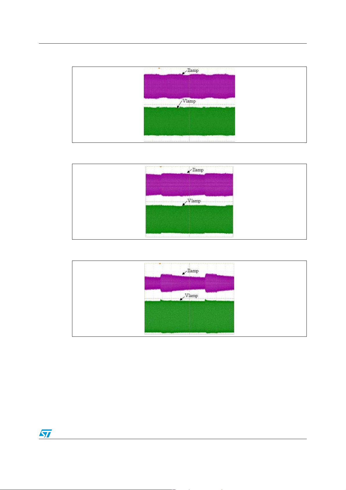
The different Ton to triac in the dimming control circuit provides the different power
dissipation to the lamp. The figures also show the negative resistance characteristics of the
lamp, such as when the lamp current decreases, the voltage increases accordingly.
Figure 17, shows us the voltage and current measurement at Ton equal to 9 ms. Figure 18,
shows us the voltage and current measurement at Ton equal to 5 ms. Figure 19 shows us
the voltage and current measurement at Ton equal to 3 ms.
12/17
Page 13
AN2590 Test results
Figure 17. Lamp voltage and current at Ton=9 ms, Vlamp=100 V/div,
Ilamp= 200 mA/div
Figure 18. Lamp voltage and current at Ton=5 ms, Vlamp=100 V/div,
Ilamp= 200 mA/div
Figure 19. Lamp voltage and current at Ton=3 ms, Vlamp=100 V/div,
Ilamp= 200 mA/div
13/17
Page 14

Conclusion AN2590
5 Conclusion
A dimmable CFL solution has been discussed and analyzed. CFLs can completely replace
incandescent lamps in dimming systems. With a dimming range of 20%-100%, CFLs are
very energy efficient and have a reliable and longer lifetime. The efficiency is above 80%
which makes this solution suitable in compact applications.
5.1 References
1. L6574D Datasheet CFL/TL ballast driver preheat and dimming
2. AN993, the application note of electronic ballast with PFC using L6574 and L6561
14/17
Page 15

AN2590 Bill of material
Appendix A Bill of material
Table 2. Bill of material
Symbol Value Note
R1 470 kΩ 0.5 W
R2 560 Ω
R3 5.1 kΩ
R4 10 kΩ
R5 100 kΩ
R6 68 kΩ
R7 68 Ω
R8 180 kΩ 0.5 W
R9 2 Ω 0.5 W
R10 22 Ω
R11 22 Ω
R12 75 kΩ
R14 10 kΩ
Rin 10 Ω
C1 10 µF 450 V, Electrolytic
C2 22 µF 25 V, Electrolytic
C3 100 nF
C4 8.2 nF
C5 100 nF
C6 680 pF C3216C0G2J681J, TDK
C7 100 nF
C8 150 nF
C9 27 pF
C10 22 µf 25 V, Electrolytic
Cf1, Cf2 33 nF 400 V, CBB
Cb 100 nF 400 V, CBB
Cr 5.6 nF 1 kV, ceramic
Lin 4.7 mH TSL1112-472JR21, TDK
L1, Lr 2.8 mH See Ta b l e 3
D1 – D4 1N4007
D5 – D6 1N4148
Db1, Db2 STTH1L06 the turbo 2 ultra fast high voltage rectifiers, STMicroelectronics
15/17
Page 16

Revision history AN2590
Table 2. Bill of material (continued)
Symbol Value Note
ZD1 15V
Q1, Q2 STD4NK50Z
IC1 L6574D high performance ballast driver, STMicroelectronics
Table 3. Specification of inductors - "L1" and "Lr"
Key item Used type
Core PC40EE16-Z or equivalent
Bobbin BE16-116CPFR
Winding AWG34 * 200 turns
Air gap ~ 0.3 mm on each leg for the inductance of 2.8 mH
6 Revision history
Table 4. Document revision history
Date Revision Changes
08-Oct-2007 1 First release
Zener protected SuperMESH™ Power MOSFET,
STMicroelectronics
16/17
Page 17

AN2590
Please Read Carefully:
Information in this document is provided solely in connection with ST products. STMicroelectronics NV and its subsidiaries (“ST”) reserve the
right to make changes, corrections, modifications or improvements, to this document, and the products and services described herein at any
time, without notice.
All ST products are sold pursuant to ST’s terms and conditions of sale.
Purchasers are solely responsible for the choice, selection and use of the ST products and services described herein, and ST assumes no
liability whatsoever relating to the choice, selection or use of the ST products and services described herein.
No license, express or implied, by estoppel or otherwise, to any intellectual property rights is granted under this document. If any part of this
document refers to any third party products or services it shall not be deemed a license grant by ST for the use of such third party products
or services, or any intellectual property contained therein or considered as a warranty covering the use in any manner whatsoever of such
third party products or services or any intellectual property contained therein.
UNLESS OTHERWISE SET FORTH IN ST’S TERMS AND CONDITIONS OF SALE ST DISCLAIMS ANY EXPRESS OR IMPLIED
WARRANTY WITH RESPECT TO THE USE AND/OR SALE OF ST PRODUCTS INCLUDING WITHOUT LIMITATION IMPLIED
WARRANTIES OF MERCHANTABILITY, FITNESS FOR A PARTICULAR PURPOSE (AND THEIR EQUIVALENTS UNDER THE LAWS
OF ANY JURISDICTION), OR INFRINGEMENT OF ANY PATENT, COPYRIGHT OR OTHER INTELLECTUAL PROPERTY RIGHT.
UNLESS EXPRESSLY APPROVED IN WRITING BY AN AUTHORIZED ST REPRESENTATIVE, ST PRODUCTS ARE NOT
RECOMMENDED, AUTHORIZED OR WARRANTED FOR USE IN MILITARY, AIR CRAFT, SPACE, LIFE SAVING, OR LIFE SUSTAINING
APPLICATIONS, NOR IN PRODUCTS OR SYSTEMS WHERE FAILURE OR MALFUNCTION MAY RESULT IN PERSONAL INJURY,
DEATH, OR SEVERE PROPERTY OR ENVIRONMENTAL DAMAGE. ST PRODUCTS WHICH ARE NOT SPECIFIED AS "AUTOMOTIVE
GRADE" MAY ONLY BE USED IN AUTOMOTIVE APPLICATIONS AT USER’S OWN RISK.
Resale of ST products with provisions different from the statements and/or technical features set forth in this document shall immediately void
any warranty granted by ST for the ST product or service described herein and shall not create or extend in any manner whatsoever, any
liability of ST.
ST and the ST logo are trademarks or registered trademarks of ST in various countries.
Information in this document supersedes and replaces all information previously supplied.
The ST logo is a registered trademark of STMicroelectronics. All other names are the property of their respective owners.
© 2007 STMicroelectronics - All rights reserved
STMicroelectronics group of companies
Australia - Belgium - Brazil - Canada - China - Czech Republic - Finland - France - Germany - Hong Kong - India - Israel - Italy - Japan -
Malaysia - Malta - Morocco - Singapore - Spain - Sweden - Switzerland - United Kingdom - United States of America
www.st.com
17/17
 Loading...