

AN2566
Application note
PM6680 evaluation kit dual step-down controller
with auxiliary voltages for notebook power system
Introduction
PM6680A evaluation kit order code: STEVAL-ISA053V1.
The PM6680 is a dual step-down controller with adju stable output voltages for notebook
computer power systems . The PM66 80 e valuation kit is designed to test the performance of
the PM6680 by employing a typical application circuit that allows testing of all PM6680
device functions. The kit features two switching sections, with (typically) 1.5 V and 1.05 V
outputs, from a 6 V to 28 V input battery voltage. The operating switching frequency of the
two switching sections is 200 kHz / 300 kHz, respectively. Each switching section delivers
more than 5 A output current. Moreover, an internal linear regulator can provide 5 V @ 100
mA peak current.
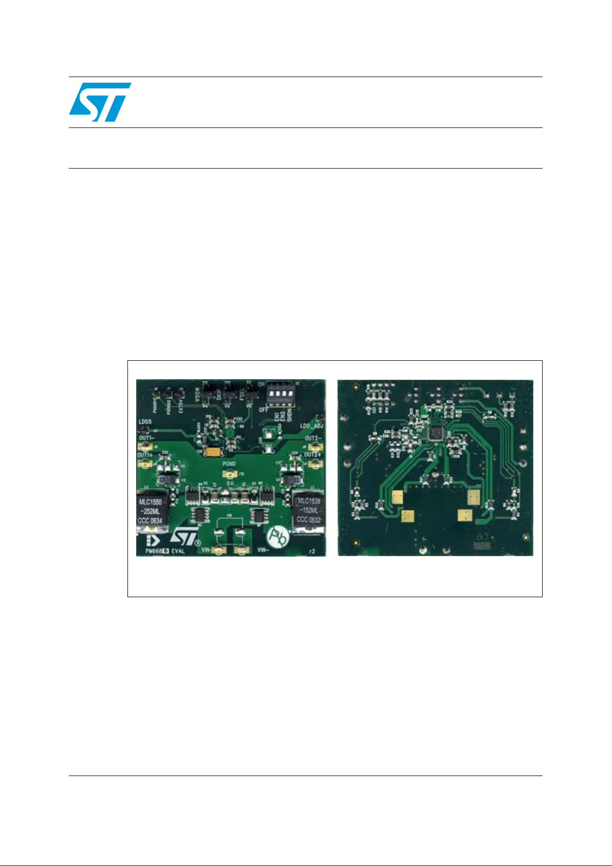
Figure 1. PM6680 evaluation kit
Top
April 2008 Rev 3 1/29
Bottom
www.st.com

Contents AN2566
Contents
1 Main features . . . . . . . . . . . . . . . . . . . . . . . . . . . . . . . . . . . . . . . . . . . . . . . 5
2 Evaluation kit schematic . . . . . . . . . . . . . . . . . . . . . . . . . . . . . . . . . . . . . 6
3 Component list . . . . . . . . . . . . . . . . . . . . . . . . . . . . . . . . . . . . . . . . . . . . . 7
4 Evaluation board layout . . . . . . . . . . . . . . . . . . . . . . . . . . . . . . . . . . . . . . 9
5 I/O interface . . . . . . . . . . . . . . . . . . . . . . . . . . . . . . . . . . . . . . . . . . . . . . . 11
6 Recommended equipment . . . . . . . . . . . . . . . . . . . . . . . . . . . . . . . . . . . 12
7 Quick start . . . . . . . . . . . . . . . . . . . . . . . . . . . . . . . . . . . . . . . . . . . . . . . . 13
8 Jumper settings . . . . . . . . . . . . . . . . . . . . . . . . . . . . . . . . . . . . . . . . . . . . 14
9 Feedback output connections . . . . . . . . . . . . . . . . . . . . . . . . . . . . . . . . 16
10 Test setup and performance summary . . . . . . . . . . . . . . . . . . . . . . . . . 17
10.1 Test setup . . . . . . . . . . . . . . . . . . . . . . . . . . . . . . . . . . . . . . . . . . . . . . . . . 17
10.2 Power-up . . . . . . . . . . . . . . . . . . . . . . . . . . . . . . . . . . . . . . . . . . . . . . . . . 17
10.3 Soft-start and shutdown waveforms . . . . . . . . . . . . . . . . . . . . . . . . . . . . . 17
10.4 1.5 V and 1.05 V output efficiency vs. load current . . . . . . . . . . . . . . . . . 19
10.5 Power consumption analysis . . . . . . . . . . . . . . . . . . . . . . . . . . . . . . . . . . 20
10.6 Switching frequency vs. load current . . . . . . . . . . . . . . . . . . . . . . . . . . . . 23
10.7 Linear regulator output voltages vs. output current . . . . . . . . . . . . . . . . . 24
10.8 Load transient responses . . . . . . . . . . . . . . . . . . . . . . . . . . . . . . . . . . . . . 24
11 Representatives waveforms . . . . . . . . . . . . . . . . . . . . . . . . . . . . . . . . . . 26
12 Revision history . . . . . . . . . . . . . . . . . . . . . . . . . . . . . . . . . . . . . . . . . . . 28
2/29

AN2566 List of figures
List of figures
Figure 1. PM6680 evaluation kit . . . . . . . . . . . . . . . . . . . . . . . . . . . . . . . . . . . . . . . . . . . . . . . . . . . . . 1
Figure 2. Evaluation kit schematic . . . . . . . . . . . . . . . . . . . . . . . . . . . . . . . . . . . . . . . . . . . . . . . . . . . . 6
Figure 3. PM6680 evaluation board layout - top layer (PGND plain and component side) . . . . . . . . . 9
Figure 4. PM6680 evaluation board layout - inner layer 1 (SGND layer and V
Figure 5. PM6680 evaluation board layout - inner layer 2 (SGND layer and signals) . . . . . . . . . . . . 10
Figure 6. PM6680 evaluation board layout - bottom layer (PM6680 and component side). . . . . . . . 10
Figure 7. REF and LDO5 power-up . . . . . . . . . . . . . . . . . . . . . . . . . . . . . . . . . . . . . . . . . . . . . . . . . . 17
Figure 8. Section 1 soft-start waveforms . . . . . . . . . . . . . . . . . . . . . . . . . . . . . . . . . . . . . . . . . . . . . . 18
Figure 9. Section 2 soft-start waveforms . . . . . . . . . . . . . . . . . . . . . . . . . . . . . . . . . . . . . . . . . . . . . . 18
Figure 10. Section 1 shutdown waveforms . . . . . . . . . . . . . . . . . . . . . . . . . . . . . . . . . . . . . . . . . . . . . 19
Figure 11. Section 2 shutdown waveforms . . . . . . . . . . . . . . . . . . . . . . . . . . . . . . . . . . . . . . . . . . . . . 19
Figure 12. 1.5 V SMPS efficiency . . . . . . . . . . . . . . . . . . . . . . . . . . . . . . . . . . . . . . . . . . . . . . . . . . . . 20
Figure 13. 1.05 V SMPS efficiency . . . . . . . . . . . . . . . . . . . . . . . . . . . . . . . . . . . . . . . . . . . . . . . . . . . 20
Figure 14. Input current vs. input voltage. . . . . . . . . . . . . . . . . . . . . . . . . . . . . . . . . . . . . . . . . . . . . . . 21
Figure 15. Input current vs. input voltage. . . . . . . . . . . . . . . . . . . . . . . . . . . . . . . . . . . . . . . . . . . . . . . 21
Figure 16. Input current vs. input voltage. . . . . . . . . . . . . . . . . . . . . . . . . . . . . . . . . . . . . . . . . . . . . . . 22
Figure 17. Device current consumption vs. input voltage . . . . . . . . . . . . . . . . . . . . . . . . . . . . . . . . . . 22
Figure 18. Device current consumption vs. input voltage . . . . . . . . . . . . . . . . . . . . . . . . . . . . . . . . . . 23
Figure 19. 1.5 V output switching frequency vs. load current . . . . . . . . . . . . . . . . . . . . . . . . . . . . . . . 23
Figure 20. 1.05 V output switching frequency vs. load current . . . . . . . . . . . . . . . . . . . . . . . . . . . . . . 24
Figure 21. LDO5 output vs. load current . . . . . . . . . . . . . . . . . . . . . . . . . . . . . . . . . . . . . . . . . . . . . . . 24
Figure 22. SMPS 1.5 V load transient response . . . . . . . . . . . . . . . . . . . . . . . . . . . . . . . . . . . . . . . . . 25
Figure 23. SMPS 1.05 V load transient response . . . . . . . . . . . . . . . . . . . . . . . . . . . . . . . . . . . . . . . . 25
Figure 24. SMPS pulse skip mode. . . . . . . . . . . . . . . . . . . . . . . . . . . . . . . . . . . . . . . . . . . . . . . . . . . . 26
Figure 25. SMPS no-audible skip mode . . . . . . . . . . . . . . . . . . . . . . . . . . . . . . . . . . . . . . . . . . . . . . . 26
Figure 26. SMPS PWM mode . . . . . . . . . . . . . . . . . . . . . . . . . . . . . . . . . . . . . . . . . . . . . . . . . . . . . . . 27
plane) . . . . . . . . . . . 9
IN
3/29

List of tables AN2566
List of tables
Table 1. Component list . . . . . . . . . . . . . . . . . . . . . . . . . . . . . . . . . . . . . . . . . . . . . . . . . . . . . . . . . . . 7
Table 2. The test points of the evaluation board. . . . . . . . . . . . . . . . . . . . . . . . . . . . . . . . . . . . . . . . 11
Table 3. Jumper S11 - V5SW pin connections. . . . . . . . . . . . . . . . . . . . . . . . . . . . . . . . . . . . . . . . . 14
Table 4. Jumper S3 - FSEL pin connections . . . . . . . . . . . . . . . . . . . . . . . . . . . . . . . . . . . . . . . . . . 14
Table 5. Jumper S10 - SKIP pin connections. . . . . . . . . . . . . . . . . . . . . . . . . . . . . . . . . . . . . . . . . . 15
Table 6. Jumper S4, S5 . . . . . . . . . . . . . . . . . . . . . . . . . . . . . . . . . . . . . . . . . . . . . . . . . . . . . . . . . . 16
Table 7. Jumper S8, S9 . . . . . . . . . . . . . . . . . . . . . . . . . . . . . . . . . . . . . . . . . . . . . . . . . . . . . . . . . . 16
Table 8. Jumper S4, S5 . . . . . . . . . . . . . . . . . . . . . . . . . . . . . . . . . . . . . . . . . . . . . . . . . . . . . . . . . . 16
Table 9. Jumper S8, S9 . . . . . . . . . . . . . . . . . . . . . . . . . . . . . . . . . . . . . . . . . . . . . . . . . . . . . . . . . . 16
Table 10. Document revision history . . . . . . . . . . . . . . . . . . . . . . . . . . . . . . . . . . . . . . . . . . . . . . . . . 28
4/29

AN2566 Main features
1 Main features
● Constant on-time control allows very fast load transients
● 6 V to 28 V input voltage range
● 5 V auxiliary output voltage
● Adjustable switching outputs
● Lossless current sensing using lo w side MOSFET R
●
Negative current limit
● Soft-start internally fixed at 2.8 ms
● Soft-end for output discharge
● 200 kHz / 300 kHz, 300 kHz / 400 kHz, 400 kHz / 500 kHz (5 V / 3 V selectable
switching frequency)
● Selectable pulse skip and no-audible skip modes at light loads
● Independent power good signals
DS(on)
5/29
Evaluation kit schematic AN2566
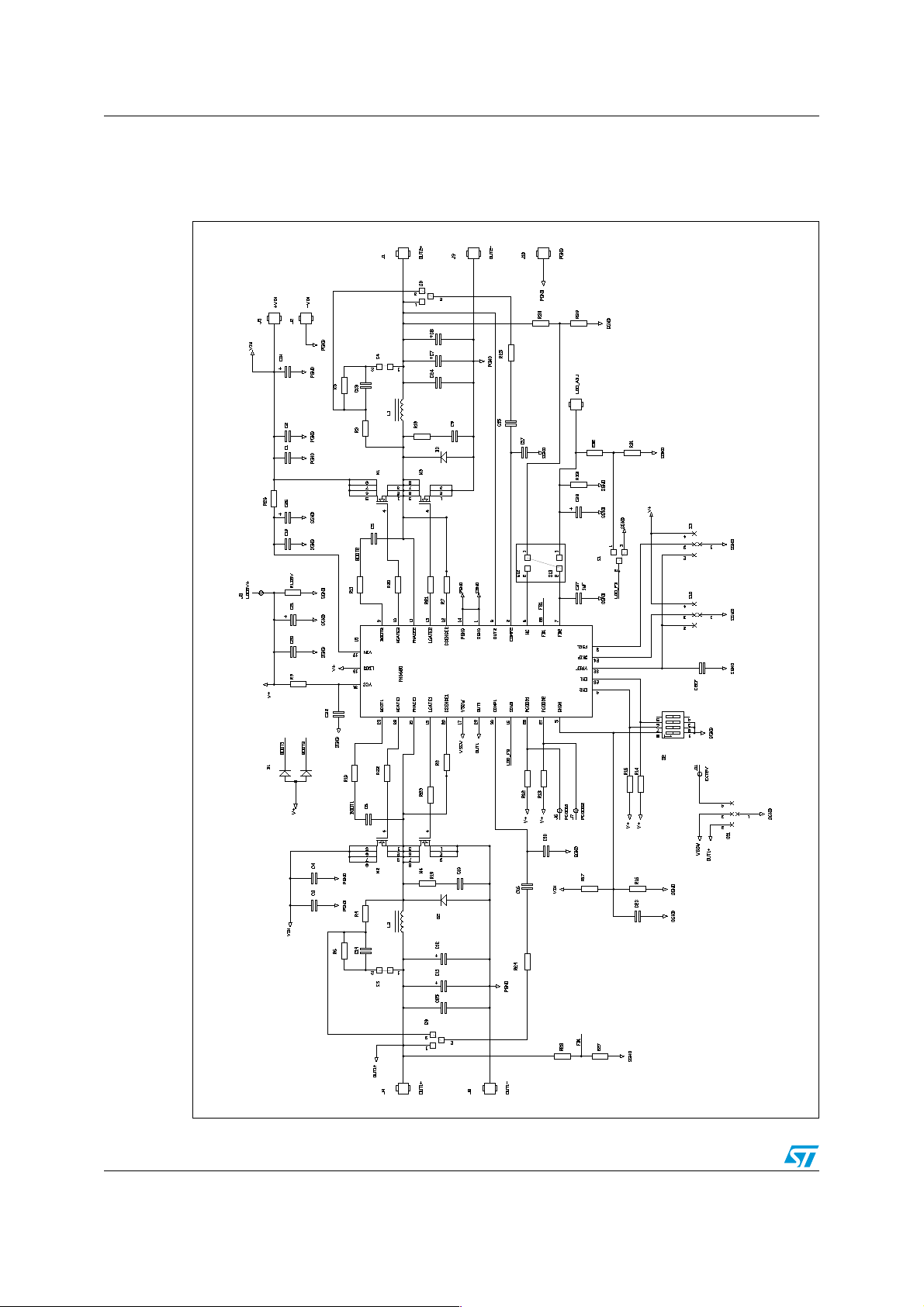
2 Evaluation kit schematic
Figure 2. Evaluation kit schematic
6/29
AN2566 Component list
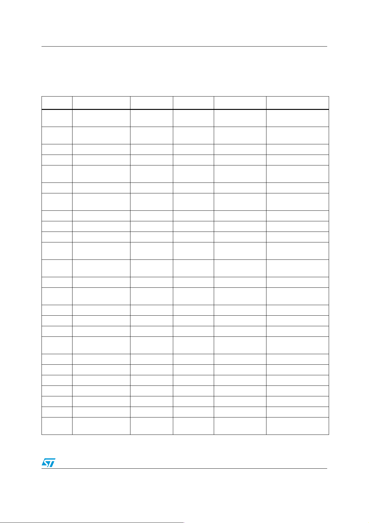
3 Component list
Table 1. Component list
Name Description Size Value Supplier Part number
C1, C2,
C3
C4
C5, C6 Ceramic capacitor 0805 0,1 µF Standard
C7 Low ESR capacitor D case Not installed Standard
C8
C11 Low ESR capacitor D case Not installed Standard
C12
C13, C14 Ceramic capacitor 0805 5.6 nF Standard
C15, C16 Ceramic capacitor 0603 1 nF Standard
C17, C18 Ceramic capacitor 0603 47 pF Standard
C19
C26
C20 Ceramic capacitor 0603 1 µF Standard
C21
C22 Ceramic capacitor 0805 220 nF Standard
Ceramic capacitor
50 V
Ceramic capacitor
50 V
Low ESR capacitor
4 V, 12 mΩ ESR
Low ESR capacitor
4 V, 12 mΩ ESR
Ceramic capacitor
50 V
Tantalum capacitor
35 V
Tantalum capacitor
package A, 16 V
1210 10 µF Taiyo Yuden UMK325BJ106KM
1210 Not installed
D case 330 µF POSCAP - Sanyo 4TPD33OM
D case 330 µF POSCAP - Sanyo 4TPD33OM
0805 0.1 µF Standard B37941K5104K62
C case 4.7 µF AVX TPS TPSC475*035#0600
B case 4.7 µF AVX THJ THJB475*016#JN
C9, C10 Ceramic capacitor 0805 Not installed Standard
C23 Ceramic capacitor 0603 10 pF Standard
CIN
CREF Ceramic capacitor 0603 100 nF Standard
C24,C25 Ceramic capacitor 0805 10 µF Standard
C27 Ceramic capacitor 0805 Not installed Standard
C28 Tantalum capacitor 3216 Not installed Standard
D1 Dual Schottky diode SOT23 STMicroelectronics BA T54A
D2,D3 Diode 1 A, 30 V DO216-AA STMicroelectronics STPS1L30M
IC1 PM6680 device
Electrolytic capacitor
39 µF, 25 V
D 10 mm Not installed Sanyo 25SVPD39M
VFQFPN-32
5 mm x 5 mm
STMicroelectronics PM6680
7/29
Component list AN2566
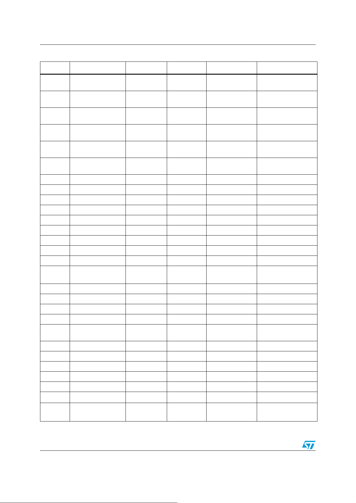
Table 1. Component list (continued)
Name Description Size Value Supplier Part number
L1
L2
M1
M2
M3
M4
R7,R8 Resistor 0805 680 Ω Standard
R3 Resistor 0805 22 kΩ Standard
R4 Resistor 0805 36 kΩ Standard
R5 Resistor 0805 3.3 kΩ Standard
R6 Resistor 0805 3 kΩ Standard
R24 Resistor 0805 1.1 kΩ Standard
R25 Resistor 0805 820 Ω Standard
R9 Resistor 0805 47 Ω Standard
R10,R11 Resistor 0805 10 Ω Standard
1.5 µH inductor, 12 A
sat.
2.5 µH inductor, 8 A
sat.
MOSFET control FET
SO-8
MOSFET control FET
SO-8
MOSFET Sync FET
SO-8
MOSFET Sync FET
SO-8
13 mm x
13 mm
13 mm x
13 mm
SO-8 STMicroelectronics STS12NH3LL
SO-8 STMicroelectronics STS12NH3LL
SO-8 STMicroelectronics STS12NH3LL
SO-8 STMicroelectronics STS12NH3LL
1.5 µH Coilcraft MLC1538-152ML
2.5 µH Coilcraft MLC1550-252ML
R12,R13,
R14,R15
R16 Resistor 0603 150 kΩ Standard
R18,R19 Resistor 0603 Not installed
R17 Resistor 0603 560 kΩ Standard
R26 Resistor 1206 3.9 Ω Standard
R20, R21,
R22, R23
R27 Resistor 0805 10 kΩ Standard
R28 Resistor 0805 6.8 kΩ Standard
R29 Resistor 0805 11 kΩ Standard
R30 Resistor 0805 1.8 kΩ Standard
R31 Resistor 0805 Not installed Standard
R32 Resistor 0805 Not installed Standard
RLD5V,
RLD3V
Resistor 0603 100 kΩ Standard
Resistor 0805 0 Ω Standard
Resistor 0805 Not installed Standard
8/29
AN2566 Evaluation board layout
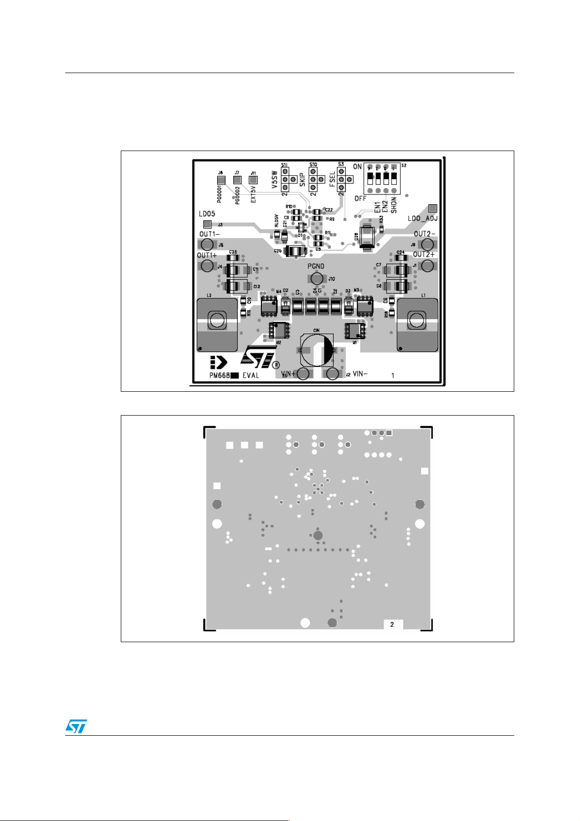
4 Evaluation board layout
Figure 3. PM6680 evaluation board layout - top layer (PGND plain and component
side)
Figure 4. PM6680 evaluation boar d la y out - inner la y er 1 (SGND la y er and V
plane)
IN
9/29
 Loading...