

Page 1
AN2565
Application note
PM6680A evaluation kit
dual step-down controller with auxiliary voltages
Introduction
PM6680A evaluation kit order code: STEVAL-ISA053V2.
The PM6680A is a dual step-do wn controller with adjustab le outp ut v oltages . The PM6680A
evaluation kit is designed to test the performance of the PM 6680A by employing a typical
application circuit that allows testing of all th e PM6680A device functions. The kit features
two switching sections, with (typically) 3.3 V and 1.8 V outputs, from a 6 V to 36 V input
voltage. The typi cal oper ating switching frequency of the two switching sections is 200 kHz /
300 kHz, respectively. Each switching section delivers more than 2.5 A of output current.
Moreover, an internal linear regulator can provide 5 V @ 100 mA peak current.
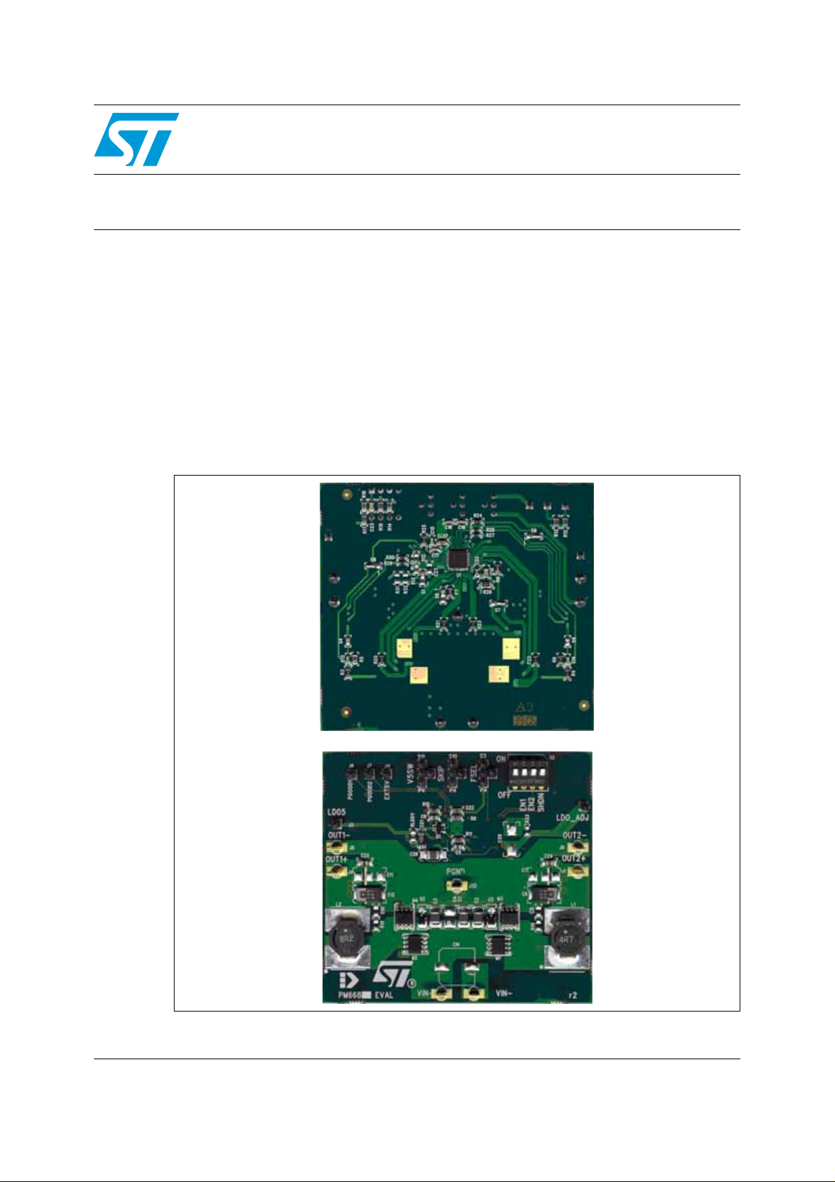
Figure 1. PM6680A evaluation kit
April 2008 Rev 2 1/29
www.st.com
Page 2

Contents AN2565
Contents
1 Main features . . . . . . . . . . . . . . . . . . . . . . . . . . . . . . . . . . . . . . . . . . . . . . . 4
2 Evaluation kit schematic . . . . . . . . . . . . . . . . . . . . . . . . . . . . . . . . . . . . . 5
3 Component list . . . . . . . . . . . . . . . . . . . . . . . . . . . . . . . . . . . . . . . . . . . . . 6
4 Evaluation board layout . . . . . . . . . . . . . . . . . . . . . . . . . . . . . . . . . . . . . . 8
5 I/O interface . . . . . . . . . . . . . . . . . . . . . . . . . . . . . . . . . . . . . . . . . . . . . . . 10
6 Recommended equipment . . . . . . . . . . . . . . . . . . . . . . . . . . . . . . . . . . . 11
7 Quick start . . . . . . . . . . . . . . . . . . . . . . . . . . . . . . . . . . . . . . . . . . . . . . . . 12
8 Jumper settings . . . . . . . . . . . . . . . . . . . . . . . . . . . . . . . . . . . . . . . . . . . . 13
9 Feedback output connections . . . . . . . . . . . . . . . . . . . . . . . . . . . . . . . . 15
10 Test setup and performance summary . . . . . . . . . . . . . . . . . . . . . . . . . 16
10.1 Test setup . . . . . . . . . . . . . . . . . . . . . . . . . . . . . . . . . . . . . . . . . . . . . . . . . 16
10.2 Power-up . . . . . . . . . . . . . . . . . . . . . . . . . . . . . . . . . . . . . . . . . . . . . . . . . 16
10.3 Soft-start and shutdown waveforms . . . . . . . . . . . . . . . . . . . . . . . . . . . . . 17
10.4 OUT1 and OUT2 output efficiency vs. load current . . . . . . . . . . . . . . . . . 19
10.5 Power consumption analysis . . . . . . . . . . . . . . . . . . . . . . . . . . . . . . . . . . 20
10.6 Switching frequency vs. load current . . . . . . . . . . . . . . . . . . . . . . . . . . . . 23
10.7 Linear regulator output voltages vs. output current . . . . . . . . . . . . . . . . . 24
10.8 Load transient response . . . . . . . . . . . . . . . . . . . . . . . . . . . . . . . . . . . . . . 24
11 Representative waveforms . . . . . . . . . . . . . . . . . . . . . . . . . . . . . . . . . . . 26
12 Revision history . . . . . . . . . . . . . . . . . . . . . . . . . . . . . . . . . . . . . . . . . . . 28
2/29
Page 3

AN2565 List of figures
List of figures
Figure 1. PM6680A evaluation kit . . . . . . . . . . . . . . . . . . . . . . . . . . . . . . . . . . . . . . . . . . . . . . . . . . . . 1
Figure 2. Evaluation kit schematic . . . . . . . . . . . . . . . . . . . . . . . . . . . . . . . . . . . . . . . . . . . . . . . . . . . . 5
Figure 3. PM6680A eval board layout - top layer (PGND plane and component side) . . . . . . . . . . . . 8
Figure 4. PM6680A eval board layout - inn er layer 1 (SGND layer and V
Figure 5. PM6680A eval board layout - inner layer 2 (SGND layer and signals). . . . . . . . . . . . . . . . . 9
Figure 6. PM6680A eval board layout - bottom layer (PM6680A and component side) . . . . . . . . . . . 9
Figure 7. Test setup connections. . . . . . . . . . . . . . . . . . . . . . . . . . . . . . . . . . . . . . . . . . . . . . . . . . . . 16
Figure 8. Power-up sequence . . . . . . . . . . . . . . . . . . . . . . . . . . . . . . . . . . . . . . . . . . . . . . . . . . . . . . 17
Figure 9. Section 1 soft-start waveforms . . . . . . . . . . . . . . . . . . . . . . . . . . . . . . . . . . . . . . . . . . . . . . 17
Figure 10. Section 2 soft-start waveforms . . . . . . . . . . . . . . . . . . . . . . . . . . . . . . . . . . . . . . . . . . . . . . 18
Figure 11. Section 1 shutdown waveforms . . . . . . . . . . . . . . . . . . . . . . . . . . . . . . . . . . . . . . . . . . . . . 18
Figure 12. Section 2 shutdown waveforms . . . . . . . . . . . . . . . . . . . . . . . . . . . . . . . . . . . . . . . . . . . . . 19
Figure 13. OUT1 efficiency . . . . . . . . . . . . . . . . . . . . . . . . . . . . . . . . . . . . . . . . . . . . . . . . . . . . . . . . . 20
Figure 14. OUT2 efficiency . . . . . . . . . . . . . . . . . . . . . . . . . . . . . . . . . . . . . . . . . . . . . . . . . . . . . . . . . 20
Figure 15. Input current vs. input voltage. . . . . . . . . . . . . . . . . . . . . . . . . . . . . . . . . . . . . . . . . . . . . . . 21
Figure 16. Input current vs. input voltage. . . . . . . . . . . . . . . . . . . . . . . . . . . . . . . . . . . . . . . . . . . . . . . 21
Figure 17. Input current vs. input voltage. . . . . . . . . . . . . . . . . . . . . . . . . . . . . . . . . . . . . . . . . . . . . . . 22
Figure 18. Device current consumption vs. input voltage . . . . . . . . . . . . . . . . . . . . . . . . . . . . . . . . . . 22
Figure 19. Device current consumption vs. input voltage . . . . . . . . . . . . . . . . . . . . . . . . . . . . . . . . . . 23
Figure 20. OUT1 switching frequency vs. load current . . . . . . . . . . . . . . . . . . . . . . . . . . . . . . . . . . . . 23
Figure 21. OUT2 switching frequency vs. load current . . . . . . . . . . . . . . . . . . . . . . . . . . . . . . . . . . . . 24
Figure 22. LDO5 output vs. load current . . . . . . . . . . . . . . . . . . . . . . . . . . . . . . . . . . . . . . . . . . . . . . . 24
Figure 23. OUT1 load transient response . . . . . . . . . . . . . . . . . . . . . . . . . . . . . . . . . . . . . . . . . . . . . . 25
Figure 24. OUT2 load transient response . . . . . . . . . . . . . . . . . . . . . . . . . . . . . . . . . . . . . . . . . . . . . . 25
Figure 25. SMPS pulse skip mode. . . . . . . . . . . . . . . . . . . . . . . . . . . . . . . . . . . . . . . . . . . . . . . . . . . . 26
Figure 26. SMPS no-audible skip mode . . . . . . . . . . . . . . . . . . . . . . . . . . . . . . . . . . . . . . . . . . . . . . . 26
Figure 27. SMPS PWM mode . . . . . . . . . . . . . . . . . . . . . . . . . . . . . . . . . . . . . . . . . . . . . . . . . . . . . . . 27
plane). . . . . . . . . . . . . . . 8
IN
3/29
Page 4

Main features AN2565
1 Main features
● Constant on-time control allows very fast load transients
● 6 V to 36 V input voltage range
● 5 V auxiliary output voltage
● Adjustable switching outputs
● Lossless current sensing using low side MOSFET R
●
Negative current limit
● Soft-start internally fixed at 2.8 ms
● Soft-end for output discharge
● 200 kHz / 300 kHz, 300 kHz / 400 kHz, 400 kHz / 500 kHz (OUT1 / OUT2 selectable
switching frequency)
● Selectable pulse skip and no-audible skip modes at light loads
● Independent power good signals
DS(on)
4/29
Page 5
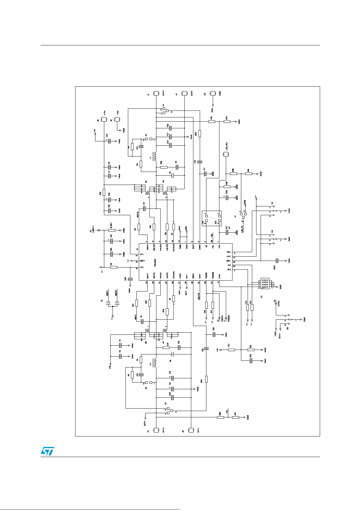
AN2565 Evaluation kit schematic
2 Evaluation kit schematic
Figure 2. Evaluation kit schematic
5/29
Page 6

Component list AN2565
3 Component list
Table 1. Component list
Qty Reference Description Value Package Part number
3 C1, C2, C3 Ceramic capacitor 10 µF, 50 V 1210 Tayio Yuden - UMK325BJ106KM
1 C4 Ceramic capacitor 10 µF, 50 V 1210
2 C5, C6 Ceramic capacitor 100 nF, 50 V 0805
1 C19 Ceramic capacitor 100 nF, 50 V 0805
1 C7 Tantalum capacitor N.M. 7343 N.M.
2 C9, C10 Ceramic capacitor N.M. 0805 N.M.
1 C11 Tantalum capacitor N.M. 7343 N.M.
1 C8 Tantalum capacitor
1 C12 Tantalum capacitor
2 C13, C14 Ceramic capacitor 10 nF, 50 V 0603
2 C15, C16 Ceramic capacitor 1.5 nF, 50 V 0603
220 µF,
25 mΩ, 6.3 V
150 µF,
18 mΩ, 4 V
7343 Sanyo POSCAP - 6TPE220M
7343 Sanyo POSCAP - 4TPE150MI
2 C17, C18 Ceramic capacitor 47 pF, 50 V 0603
1 C20 Ceramic capacitor 1 µF, 10 V 0805
1 C21 Tantalum capacitor 4.7 µF, 16 V 3216
1 C22 Ceramic capacitor 220 nF, 10 V 0805
1 C23 Ceramic capacitor 10 pF, 50 V 0805
1 CIN Tantalum capacitor N.M. D = 10 mm
1 CREF Ceramic capacitor 100 nF, 50 V 0805
1 C26 Ceramic capacitor 4.7 µF, 50 V 1210 Taiyo-Y uden - UMK325F475ZH
1 C24, C25 Ceramic capacitor 10 µF, 6.3 V 0805
1 C27 Tantalum capacitor N.M. 0805
1 C28 Tantalum capacitor N.M. 3216
1D1
2D2, D3
1 IC1 PM6680A VFQFPN-32 5x5 ST - PM6680A
1 L1 Power inductor 4.7 µH, 4 A 10 mm x 10 mm Wurth - TPC 7440650047
1 L2 Power inductor 8.2 µH, 3 A 10 mm x 10 mm Wurth - TPC 7440650082
Dual Schottky
diode
Power Schottky
rectifier
SOT23 ST - BAS70
SMA STPS1L30M
4M1, M2
6/29
>40 V N-channel
MOSFET
SO-8 ST - STS5NF60L
Page 7

AN2565 Component list
Table 1. Component list (continued)
Qty Reference Description Value Package Part number
4M3, M4
1 R3 Resistor 1% 20 kΩ 0805
1 R4 Resistor 1% 47 kΩ 0805
1 R5 Resistor 1% 2.2 kΩ 0805
1 R6 Resistor 1% 1.1 kΩ 0805
2 R7, R8 Resistor 1% 390 Ω 0805
1 R9 Resistor 1% 47 Ω 0805
2 R10, R11 Resistor 1% 10 Ω 0805
4 R12:R15 Resistor 1% 100 kΩ 0805
1 R16 Resistor 1% 43 kΩ 0805
1 R17 Resistor 1% 510 kΩ 0805
2 R18, R19 Resistor 1% N.M. 0805
R20, R21,
4
R22, R23
1 R24 Resistor 1% 1.1 kΩ 0805
1 R25 Resistor 1% 820 Ω 0805
1 R26 Resistor 1% 3.9 Ω 1206
> 40 V N-channel
MOSFET
Resistor 1% 0Ω 0805
SO-8 ST - STS7NF60L
1 R27 Resistor 1% 10 kΩ 0805
1 R29 Resistor 1% 10 kΩ 0805
1 R28 Resistor 1% 27 kΩ 0805
1 R30 Resistor 1% 10 kΩ 0805
1 R31 Resistor 1% N.M: 0603
1 R32 Resistor 1% N.M. 0603
1 R33 Resistor 1% N.M. 0805
1
RLD5V,
RLD3V
Resistor N.M. 0805
7/29
Page 8
Evaluation board layout AN2565
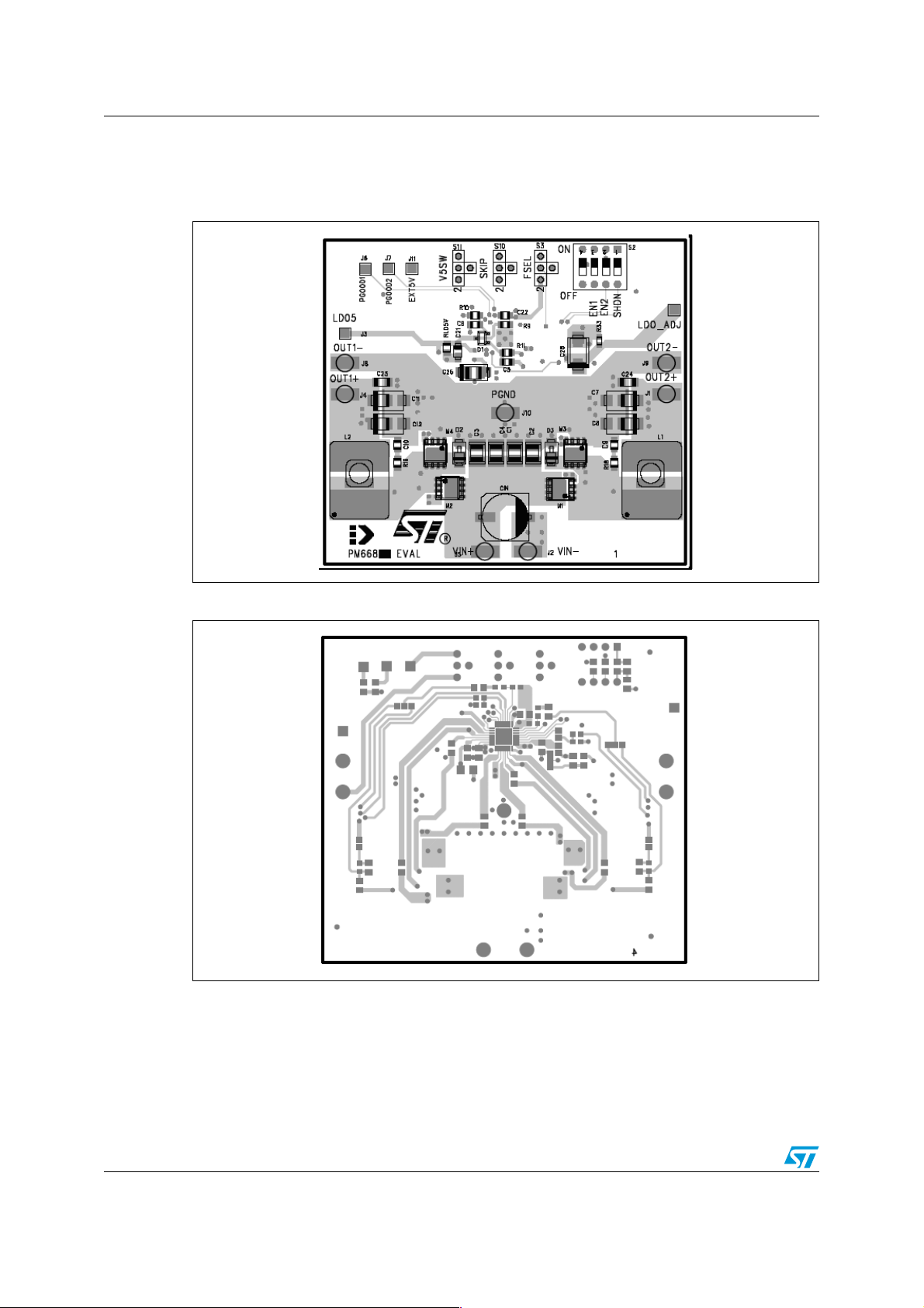
4 Evaluation board layout
Figure 3. PM6680A eval board layout - top layer (PGND plane and component side)
Figure 4. PM6680A eval board layout - inner layer 1 (SGND layer and V
plane)
IN
8/29
Page 9
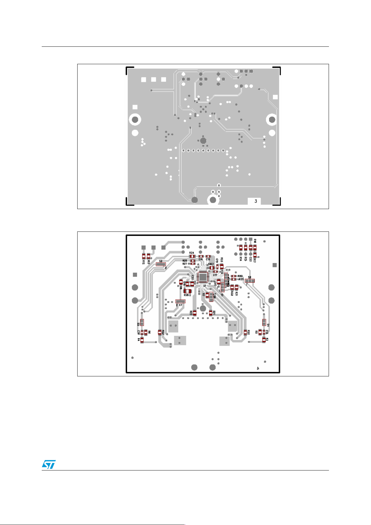
AN2565 Evaluation board layout
Figure 5. PM6680A eval board layout - inner layer 2 (SGND layer and signals)
Figure 6. PM6680A eval board layout - bottom layer (PM6680A and component
side)
9/29
Page 10

I/O interface AN2565
5 I/O interface
The evaluation board has the following test points.
Table 2. Test points of the evaluation board
Test point Description
V
+ Input voltage
IN
- Input voltage ground
V
IN
LDO5 5 V linear regulator output
LDO_ADJ Not used for this device
EXT5V 5 V external input
OUT1+ OUT1 switching section output
OUT1- OUT1 switching section output ground
PGOOD1 OUT1 switching section power good
OUT2+ OUT2 switching section output
OUT2+ OUT2 switching section output ground
PGOOD2 OUT2 switching section power good
J10 Junction pin between PGND and SGND planes
10/29
Page 11

AN2565 Recommended equipment
6 Recommended equipment
● 6 V to 36 V power supply, notebook computer battery or AC adapter
● Active loads
● Digital multimeter
● 500 MHz four-trace oscilloscope
11/29
Page 12

Quick start AN2565
7 Quick start
1. Connect the VIN+ and VIN- test points of the evaluation board to an external power
supply.
2. Ensure that all DIP switches (S2) are in the "OFF" position. In this condition all outputs
are disabled (shutdown mode).
3. Move switch S2
(standby mode).
4. Move switch S2
begins regulation of the output. PGOOD1 pin goes high after soft-start.
5. Move switch S2
begins regulation of the output. PGOOD2 pin goes high after soft-start.
6. In order to load the switching outputs, the loads must be connected between the "+"
and the "-" output test points, respectively.
7. In order to load the linear outputs, the loads must be connected between J10 and
LDO5 or alternative RLD5V resistors can be used on the evaluation board.
to the “ON” position (SHDN pin high). This turns on the LDO5 output
1
to the “ON” position (EN1 pin high). The 1.5 V switching controller
2
to the “ON” position (EN2 pin high). The 1.05 V switching controller
3
12/29
Page 13

AN2565 Jumper settings
8 Jumper settings
It is possible to select different working conditions by using the jumpers on the board.
Note: Jumpers S1, S12 and S13 are already soldered on the evaluation board and it is not
necessary to change them. Please refer to the schemat ic to verify their proper connection.
The external bypass connections for the linear regulator LDO5 are set by connecting the
V5SW pin to jumper S11 as indicated in Table 3 below.
Table 3. Jumper S11 - V5SW pin connections
Position LDO5 working conditions
OUT5V
SGND
EXT5V
When the main output voltage is greater than the boostrap-switchover
threshold, an internal 3 Ω (max) P-channel MOSFET switch connects the
V5SW pin to the LDO5 pin, shutting down the LDO5 internal linear
regulator. If not used, it must be tied to ground.
The internal linear regulator LDO5 is always on. In this case, LDO5
supplies all gate drivers and the internal circuitry. It can provide an output
peak current of 100 mA.
The internal linear regulator LDO5 remains off if an alternative 5 V ex ternal
voltage is applied to the EXT5V test point. An internal 3 Ω (max) P-channel
MOSFET switch connects the V5SW pin to the LDO5 output. The gate
drivers and internal circuitry are supplied by the same 5 V e xternal voltage
applied.
The FSEL pin is connected to jumper S3 to select the SMPS frequency. The jumper
positions and corresponding frequencies are shown in Table 4 below.
Table 4. Jumper S3 - FSEL pin connections
Position SMPS OUT1 SMPS OUT2
SGND
200 kHz 300 kHz
VREF
300 kHz 400 kHz
LDO5
400 kHz 500 kHz
To select the switching operation mod e of the SMPS , connect the SKIP pin to jumper S10 as
described in Table 5.
13/29
Page 14

Jumper settings AN2565
Table 5. Jumper S10 - SKIP pin connections
Position Switching operating mode
GND
VREF
LDO5
If the SKIP pin is tied to ground, a pulse skip mode takes place at light
loads. A zero crossing comparator prev ents the in ductor current fr om going
negative.
If the SKIP pin is tied to VREF pin enables a pulse skip mode with a
minimum switching frequency about 25 kHz (ultrasonic mode).
If the SKIP pin is tied to 5 V, The fixed PWM mode takes place. The
switching output is in a position to sink and source current from the load.
14/29
Page 15

AN2565 Feedback output connections
9 Feedback output connections
Table 6 and Table 7 below illustrate jumper settings for a loop compensation network for
very low output voltage ripple.
Table 6. Jumper S4, S5
Position Output ripple compensation
Short
Virtual ESR output ripple is generated by using a compensation network connected
between the output and the PHASE pin of the switching section.
Table 7. Jumper S8, S9
Position Feedback connection
Controller feedback signal connected to the compensation network
Table 8 and Table 9 describe the settings for a loop compensation network for high output
voltage ripple.
Table 8. Jumper S4, S5
Position Output ripple compensation
Open ESR output ripple is used.
Table 9. Jumper S8, S9
Position Feedback connection
Controller feedback signal connected directly to the output capacitor.
15/29
Page 16

Test setup and performance summary AN2565
10 Test setup and performance summary
10.1 Test setup
The PM6680A evaluation board has the following input/output connections:
– 24 V input through J5-J2 (V
– 3.3 V SMPS output through J4-J13 (OUT1+ and OUT1-)
– 1.8 V SMPS output through J1-J12 (OUT2+ and OUT2-)
– 5 V linear regulator output through J3 (LDO5)
Figure 7. T est setup connections
+ and VIN-)
IN
A power supply capab le of supplying at least 6 A should b e connected to V
active loads should be connected respectively to OUT1+, OUT1- and OUT2+, OUT2-.
10.2 Power-up
As shown in Figure 8, the power-up starts when the input voltage is applied and the voltage
on the SHDN pin is above the de vice “ on” threshold. First, the LDO5 go es up with a maskin g
time of about 4 ms.
+, VIN-, and two
IN
16/29
Page 17

AN2565 Test setup and performance summary
Figure 8. Power-up sequence
10.3 Soft-start and shutdown waveforms
Figures 9 and 10, and figures 11 and 12 show the soft-start and shutdown waveforms,
respectively.
The PM6680A has an independent internal digital soft-start for each switching section.
During the soft-start phase the internal current limit increases from 25% to 100%, in
increments of 25%, to avoid the inductor current reaching too high a value.
Figure 9. Section 1 soft-star t waveforms
17/29
Page 18

Test setup and performance summary AN2565
Figure 10. Section 2 soft-start waveforms
Driving the SHDN pin below the SHDN device “off” threshold will cause the device to enter
shutdown mode. In this case the switching outputs are connect ed to ground through an
internal 12
Ω power MOSFET and are discharged softly, (discharge mode). When the output
voltages reach 0.3 V, the low side MOSFETs are t urned on, quickly discharging them to
ground.
Figure 11. Section 1 shutdown waveforms
OUT1
Lgate1
EN1
18/29
Page 19

AN2565 Test setup and performance summary
Figure 12. Section 2 shutdown waveforms
OUT2
Lgate2
EN2
10.4 OUT1 and OUT2 output efficiency vs. load current
Figure 13 and Figure 14 show the efficiency versus load current for different input voltage
values in PWM mode, skip mo de and no audible skip mode.
19/29
Page 20

Test setup and performance summary AN2565
Figure 13. OUT1 efficiency
OUT1=3.3V Efficiency
100
90
80
70
60
50
40
30
Efficiency [%]
20
10
0
0.001 0.010 0.100 1.000 10.000
Figure 14. OUT2 efficiency
100
90
80
70
60
50
40
30
Efficiency [%]
20
10
0
0.001 0.010 0.100 1.000 10.000
SKIP @ 12V
SKIP @ 24V
SKIP @ 32V
NO AU D. SKIP @ 12V
NO AU D. SKIP @ 24V
NO AU D. SKIP @ 32V
PWM @ 12V
PWM @ 24V
PWM @ 32V
Load curr ent [A]
OUT2=1.8V Efficiency
SKIP @ 12V
SKIP @ 24V
SKIP @ 32V
NO AU D. SKIP @ 12V
NO AU D. SKIP @ 24V
NO AU D. SKIP @ 32V
PWM @ 12V
PWM @ 24V
PWM @ 32V
Load current [ A]
10.5 Power consumption analysis
To measure the device consumption under real working conditions, an external power
supply of +5 V is connected to EXT5V.
The two traces on figures that f ollo w show the dif fe rentiation betw een the two inp ut currents.
Once the internal linear regulator is turned on, device consumption will increase as a
consequence.
Figure 15 shows the input current consumption measured at V
the input device current consumpt ion measured at the VCC pin. Both switching sections are
working in forced PWM mode. No load is applied on the outputs.
20/29
+ (including ISHDN) and
IN
Page 21

AN2565 Test setup and performance summary
Figure 15. Input current vs. input voltage
Figure 16 shows the input current measured at VIN+(includes ISHDN) and the input device
current consumption measured at the VCC pin (IEXT5V). Both switching sections are
working in SKIP mode. No load is applied.
Figure 16. Input current vs. input voltage
Figure 17 shows the input current measured at VIN+(includes ISHDN) and the input device
current consumption measured at the VCC pin (IEXT5V). Both switching sections are
working in NO-AUDIBLE SKIP mode. No load is applied.
21/29
Page 22

Test setup and performance summary AN2565
Figure 17. Input current vs. input voltage
In the following il lustr ations , the device current consumption is measured in shutdown mode
and standby mode. In shutdown mode all outputs are off (SHDN pin low). In standby mode
only the linear regulator output is on (V5SW = SGND, SHDN pin high, EN5 and EN3 pins
low).
Figure 18. Device current consumption vs. input voltage
SHUT D OWN M ODE INPUT B AT TERY CURRENT
25.00
20.00
15.00
10.00
5.00
INPUT CURRENT [uA]
0.00
8 10121416182022242628
vs INPUT VO LTAGE
INPUT VOLTA GE [V]
22/29
Page 23

AN2565 Test setup and performance summary
Figure 19. Device current consumption vs. input voltage
STANDBY MO DE INPUT BATTE RY CURRENT
184
182
180
178
176
174
INPUT CURRENT [uA]
172
8 10121416182022242628
vs INPUT VOLTAGE
INPUT VOLTAGE [V]
10.6 Switching frequency vs. load current
Figure 20 and Figure 21 show the switching frequency variation with the load current in
PWM mode, skip mode and no-audible skip mode. 12 V is applied at the V
points.
+ and VIN- test
IN
Figure 20. OUT1 switching frequency vs. load current
OUT1=3.3V Switching Frequency
250
200
150
100
fs w [kHz]
50
0
0.01 0.10 1.00 10.00
Load current [ A ]
SKIP @ 12V
SKIP @ 24V
SKIP @ 32V
NO AUD. SKIP @ 12V
NO AUD. SKIP @ 24V
NO AUD. SKIP @ 32V
PWM @ 12V
PWM @ 24V
PWM @ 32V
23/29
Page 24

Test setup and performance summary AN2565
[mA]
Figure 21. OUT2 switching frequency vs. load current
OUT2 =1.8 V Switching Frequency
300
SKIP @ 12V
fs w [kH z]
250
200
150
100
50
SKIP @ 24V
SKIP @ 32V
NO AUD. SKI P @ 12V
NO AUD. SKI P @ 24V
NO AUD. SKI P @ 32V
PWM @ 12V
PWM @ 24V
PWM @ 32V
0
0.01 0.10 1.00 10.00
Load current [A]
10.7 Linear regulator output voltages vs. output current
Figure 22 shows the load regulation for the internal linear regulator LDO5. Both switching
sections are disabled and 12 V is applied at V
+ and VIN- test points.
IN
Figure 22. LDO5 output vs. load current
LDO5 v s . OUT PUT CURRENT
4.9890
4.9880
4.9870
4.9860
4.9850
4.9840
[V]
4.9830
4.9820
4.9810
4.9800
LIN E AR OUPU T V OLTAGE
4.9790
0 102030405060708090100
10.8 Load transient response
The following figures show the load transient response from 1 A to 4 A for both switching
outputs. In each of these cases the PM6680A works in forced PWM mode (the SKIP pin is
high).
LOAD CURRENT
24/29
Page 25

AN2565 Test setup and performance summary
Figure 23. OUT1 load transient response
Figure 24. OUT2 load transient response
25/29
Page 26

Representative waveforms AN2565
11 Representative waveforms
The following illustrations show the relevant waveforms of a switching section and are
provided to underline the behavior of the device in pulse skip mode, no-audible skip mode
and forced PWM mode working conditions.
Figure 25. SMPS pulse skip mode
Figure 26. SMPS no-audible skip mode
26/29
Page 27

AN2565 Representative waveforms
Figure 27. SMPS PWM mode
27/29
Page 28

Revision history AN2565
12 Revision history
Table 10. Document revision history
Date Revision Changes
9-Aug-2007 1 Initial release
– Changed: Figure 1, 2, 3, 4, 6, 8, 9, 10
07-Apr-2008 2
– Modified: Table 1
– Minor text changes
28/29
Page 29

AN2565
Please Read Carefully:
Information in this document is provided solely in connection with ST products. STMicroelectronics NV and its subsidiaries (“ST”) reserve the
right to make changes, corrections, modifications or improvements, to this document, and the products and services described herein at any
time, without notice.
All ST products are sold pursuant to ST’s terms and conditions of sale.
Purchasers are solely res ponsibl e fo r the c hoic e, se lecti on an d use o f the S T prod ucts and s ervi ces d escr ibed he rein , and ST as sumes no
liability whatsoever relati ng to the choice, selection or use of the ST products and services described herein.
No license, express or implied, by estoppel or otherwise, to any intellectual property rights is granted under this document. If any part of this
document refers to any third pa rty p ro duc ts or se rv ices it sh all n ot be deem ed a lice ns e gr ant by ST fo r t he use of su ch thi r d party products
or services, or any intellectua l property c ontained the rein or consi dered as a warr anty coverin g the use in any manner whats oever of suc h
third party products or servi ces or any intellectual property contained therein.
UNLESS OTHERWISE SET FORTH IN ST’S TERMS AND CONDITIONS OF SALE ST DISCLAIMS ANY EXPRESS OR IMPLIED
WARRANTY WITH RESPECT TO THE USE AND/OR SALE OF ST PRODUCTS INCLUDING WITHOUT LIMITATION IMPLIED
WARRANTIES OF MERCHANTABILITY, FITNESS FOR A PARTICUL AR PURPOS E (AND THEIR EQUIVALE NTS UNDER THE LAWS
OF ANY JURISDICTION), OR INFRINGEMENT OF ANY PATENT, COPYRIGHT OR OTHER INTELLECTUAL PROPERTY RIGHT.
UNLESS EXPRESSLY APPROVED IN WRITING BY AN AUTHORIZED ST REPRESENTATIVE, ST PRODUCTS ARE NOT
RECOMMENDED, AUTHORIZED OR WARRANTED FOR USE IN MILITARY, AIR CRAFT, SPACE, LIFE SAVING, OR LIFE SUSTAINING
APPLICATIONS, NOR IN PRODUCTS OR SYSTEMS WHERE FAILURE OR MALFUNCTION MAY RESULT IN PERSONAL INJ URY,
DEATH, OR SEVERE PROPERTY OR ENVIRONMENTAL DAMAGE. ST PRODUCTS WHICH ARE NOT SPECIFIED AS "AUTOMOTIVE
GRADE" MAY ONLY BE USED IN AUTOMOTIVE APPLICATIONS AT USER’S OWN RISK.
Resale of ST products with provisions different from the statements and/or technical features set forth in this document shall immediately void
any warranty granted by ST fo r the ST pro duct or serv ice describe d herein and shall not cr eate or exten d in any manne r whatsoever , any
liability of ST.
ST and the ST logo are trademarks or registered trademarks of ST in various countries.
Information in this document su persedes and replaces all information previously supplied.
The ST logo is a registered trademark of STMicroelectronics. All other names are the property of their respective owners.
© 2008 STMicroelectronics - All rights reserved
STMicroelectronics group of compan ie s
Australia - Belgium - Brazil - Canada - China - Czech Republic - Finland - France - Germany - Hong Kong - India - Israel - Italy - Japan -
Malaysia - Malta - Morocco - Singapore - Spain - Sweden - Switzerland - United Kingdom - United States of America
www.st.com
29/29
 Loading...