

Page 1

AN2559
Application note
System power supply board for digital solutions
Introduction
This document describes a power supply reference board designed for powering digital
applications, such as CPUs, FPGAs, memories, etc. The main purpose of the board is to
illustrate the basic principles used for the design of the power supply and to give designers a
usable prototype for testing and use.
The trend in recent years in the supplying of power to MCUs, CPUs, memories, FPGAs, etc.
is to reduce the supply voltage, increase the supply current and provide different voltage
levels for different devices in one platform. A typical example of this situation is the FPGA.
The FPGA contains a core part which works at a low level voltage, the interface part placed
between the core and the output, the system part, etc. It is important to note that each
FPGA family has a slightly different voltage level and the trend is to decrease the voltage for
each new family. The lowest operating voltage currently available is 1 V, and this can be
expected to decrease to 0.9 V or 0.8 V in the near future. A similar situation exists with other
digital applications. Typically, the main CPU, memory and interfaces require different supply
voltage levels. Low operating voltages also present another challenge - transient. Digital
devices are typically sensitive to voltage level. If the voltage drops below or crosses over a
specific limit, the device is reset. This limit is typically ± 3 or ± 5%. On the other hand, digital
device consumption can change very quickly (several amps in a few hundred nanoseconds).
A power supply must be able to react very quickly with a minimum of over (or under) voltage,
especially in cases where very low output voltage is required. There is additional stress
placed on power supplies for digital applications in the industrial environment.
The industrial standard bus is 24 V, but this voltage fluctuates and the maximum input
voltage level required can reach 36 V. Additional surge protection is also a mandatory part of
power supply input for industrial applications.
The goal of the board described in this application note is to cover all of the issues outlined
above. It is intended mainly to satisfy industrial input requirements (operating voltages up to
36 V) and generate several output voltages for mid-range power applications (up to several
amps). The main output voltage level can simply be set.
September 2007 Rev 1 1/35
www.st.com
Page 2

Contents AN2559
Contents
1 Main characteristics . . . . . . . . . . . . . . . . . . . . . . . . . . . . . . . . . . . . . . . . . 4
2 Description . . . . . . . . . . . . . . . . . . . . . . . . . . . . . . . . . . . . . . . . . . . . . . . . . 5
2.1 Input part . . . . . . . . . . . . . . . . . . . . . . . . . . . . . . . . . . . . . . . . . . . . . . . . . . 6
3 PM6680A block . . . . . . . . . . . . . . . . . . . . . . . . . . . . . . . . . . . . . . . . . . . . . 7
3.0.1 Power management block . . . . . . . . . . . . . . . . . . . . . . . . . . . . . . . . . . . . 8
3.0.2 Start-up/enable block . . . . . . . . . . . . . . . . . . . . . . . . . . . . . . . . . . . . . . . . 8
3.0.3 Step-down parts . . . . . . . . . . . . . . . . . . . . . . . . . . . . . . . . . . . . . . . . . . . 10
3.1 DC-DC converters based on the L5970AD . . . . . . . . . . . . . . . . . . . . . . . 14
3.2 Reset circuit . . . . . . . . . . . . . . . . . . . . . . . . . . . . . . . . . . . . . . . . . . . . . . . 16
4 PCB layout . . . . . . . . . . . . . . . . . . . . . . . . . . . . . . . . . . . . . . . . . . . . . . . . 18
5 Bill of materials . . . . . . . . . . . . . . . . . . . . . . . . . . . . . . . . . . . . . . . . . . . . 19
6 Measurements . . . . . . . . . . . . . . . . . . . . . . . . . . . . . . . . . . . . . . . . . . . . . 23
6.1 PM6680A block - measurements . . . . . . . . . . . . . . . . . . . . . . . . . . . . . . . 23
6.1.1 Efficiency and light load consumption modes . . . . . . . . . . . . . . . . . . . . 23
6.1.2 Output voltage ripple . . . . . . . . . . . . . . . . . . . . . . . . . . . . . . . . . . . . . . . 24
6.1.3 Start-up sequence . . . . . . . . . . . . . . . . . . . . . . . . . . . . . . . . . . . . . . . . . 27
6.1.4 Transient response . . . . . . . . . . . . . . . . . . . . . . . . . . . . . . . . . . . . . . . . 27
6.2 L5970AD blocks - measurements . . . . . . . . . . . . . . . . . . . . . . . . . . . . . . 29
6.2.1 Efficiency . . . . . . . . . . . . . . . . . . . . . . . . . . . . . . . . . . . . . . . . . . . . . . . . 29
6.2.2 Output voltage ripple . . . . . . . . . . . . . . . . . . . . . . . . . . . . . . . . . . . . . . . 30
6.2.3 Transient . . . . . . . . . . . . . . . . . . . . . . . . . . . . . . . . . . . . . . . . . . . . . . . . 33
7 References . . . . . . . . . . . . . . . . . . . . . . . . . . . . . . . . . . . . . . . . . . . . . . . . 34
8 Revision history . . . . . . . . . . . . . . . . . . . . . . . . . . . . . . . . . . . . . . . . . . . 34
2/35
Page 3

AN2559 List of figures
List of figures
Figure 1. The STEVAL-PSQ001V1 demo board . . . . . . . . . . . . . . . . . . . . . . . . . . . . . . . . . . . . . . . . . 5
Figure 2. Block diagram of System Supply board . . . . . . . . . . . . . . . . . . . . . . . . . . . . . . . . . . . . . . . . 5
Figure 3. Schematic of input part . . . . . . . . . . . . . . . . . . . . . . . . . . . . . . . . . . . . . . . . . . . . . . . . . . . . . 6
Figure 4. Location and correct polarity of the input supply connector on the board . . . . . . . . . . . . . . 6
Figure 5. Electrical diagram of the PM6680A section . . . . . . . . . . . . . . . . . . . . . . . . . . . . . . . . . . . . . 7
Figure 6. The placement of the jumpers for start-up/enable settings. . . . . . . . . . . . . . . . . . . . . . . . . . 9
Figure 7. Skip mode connector . . . . . . . . . . . . . . . . . . . . . . . . . . . . . . . . . . . . . . . . . . . . . . . . . . . . . 10
Figure 8. Output connector . . . . . . . . . . . . . . . . . . . . . . . . . . . . . . . . . . . . . . . . . . . . . . . . . . . . . . . . 11
Figure 9. Jumper placement for V
Figure 10. Jumper placement for V
Figure 11. Output voltages of L5970A parts . . . . . . . . . . . . . . . . . . . . . . . . . . . . . . . . . . . . . . . . . . . . 14
Figure 12. Schematic of the two SMPS’s based on the L5970AD . . . . . . . . . . . . . . . . . . . . . . . . . . . . 15
Figure 13. Jumper placement for enable/disable function of analog output and output3 . . . . . . . . . . 16
Figure 14. Schematic of the reset circuit and board placement . . . . . . . . . . . . . . . . . . . . . . . . . . . . . . 17
Figure 15. PCB top layer layout and first internal layer . . . . . . . . . . . . . . . . . . . . . . . . . . . . . . . . . . . . 18
Figure 16. PCB second internal layer and bottom layer layout . . . . . . . . . . . . . . . . . . . . . . . . . . . . . . 18
Figure 17. Efficiency of the dual step-down converter at full load . . . . . . . . . . . . . . . . . . . . . . . . . . . . 23
Figure 18. PM6680A consumption at no load condition, in the different modes . . . . . . . . . . . . . . . . . 24
Figure 19. Output voltage ripple in different modes of light load operation . . . . . . . . . . . . . . . . . . . . . 24
Figure 20. Output voltage ripple of V
Figure 21. Output voltage ripple of V
Figure 22. Output voltage ripple of V
Figure 23. Output voltage ripple of V
Figure 24. Start-up without setting the sequence . . . . . . . . . . . . . . . . . . . . . . . . . . . . . . . . . . . . . . . . 26
Figure 25. Start-up with a set sequence . . . . . . . . . . . . . . . . . . . . . . . . . . . . . . . . . . . . . . . . . . . . . . . 26
Figure 26. Load transient response on V
Figure 27. Load transient response on V
Figure 28. Efficiency of output 3, by input voltage level . . . . . . . . . . . . . . . . . . . . . . . . . . . . . . . . . . . . 29
Figure 29. Efficiency of analog output, by input voltage level . . . . . . . . . . . . . . . . . . . . . . . . . . . . . . . 30
Figure 30. Analog 5 V - output voltage ripple. . . . . . . . . . . . . . . . . . . . . . . . . . . . . . . . . . . . . . . . . . . . 30
Figure 31. V
- output voltage ripple . . . . . . . . . . . . . . . . . . . . . . . . . . . . . . . . . . . . . . . . . . . . . . . . 31
SYS
Figure 32. Analog 3.3 V - output voltage ripple . . . . . . . . . . . . . . . . . . . . . . . . . . . . . . . . . . . . . . . . . . 31
Figure 33. V
2.5 V - output voltage ripple. . . . . . . . . . . . . . . . . . . . . . . . . . . . . . . . . . . . . . . . . . . . 32
AUX
Figure 34. Transient response of V
Figure 35. Transient response of V
voltage level setting . . . . . . . . . . . . . . . . . . . . . . . . . . . . . . . 12
CORE
voltage level setting . . . . . . . . . . . . . . . . . . . . . . . . . . . . . . . . . 13
I/O
at the minimum input voltage (5 V) . . . . . . . . . . . . . . . . . . 25
CORE
at the maximum output voltage (36 V) . . . . . . . . . . . . . . . 25
CORE
at the minimum input voltage (5 V) . . . . . . . . . . . . . . . . . . . . 25
I/O
at the maximum input voltage (36 V). . . . . . . . . . . . . . . . . . . 26
I/O
output . . . . . . . . . . . . . . . . . . . . . . . . . . . . . . . . . . . . . 27
CORE
output . . . . . . . . . . . . . . . . . . . . . . . . . . . . . . . . . . . . . . . 28
I/O
based on the L5970AD . . . . . . . . . . . . . . . . . . . . . . . . . . . . . 33
SYS
generated by the LDO KF25 . . . . . . . . . . . . . . . . . . . . . . . . . 33
AUX
3/35
Page 4
Main characteristics AN2559
1 Main characteristics
The main characteristics of the SMPS are listed below:
● Input: 5 V - 36 V DC, surge protection
● Outputs: the performance of the 6 outputs are described in Tab le 1 below.
Table 1. Output voltages (positive version)
Label V
Output1 (V
) Selectable from:
CORE
0.9, 1.0, 1.2, 1.5, 1.8 or 2.5 V
Output2 (V
) Selectable from:
I/O
1.0, 1.2, 1.5, 1.8, 2.5 V or 3.3 V
Output3 V
Output3 V
SYS
AUX
3.3 V 0.4 A (0.8 A peak) 4%
2.5 V 0.4 A 2%
OUT
4 A continuous
6 A peak
2 A continuous
3 A peak
I
max Tolerance
OUT
3%
3%
Analog 5 V 5 V 0.8 A 4%
Analog 3.3 V 3.3 V 0.15 A 2%
4/35
Page 5
AN2559 Description
2 Description
The System Supply board described in this application note is a dedicated design which
illustrates a typical solution for complete system supply, and can also be used as a direct
supply for customer solutions during the design process.
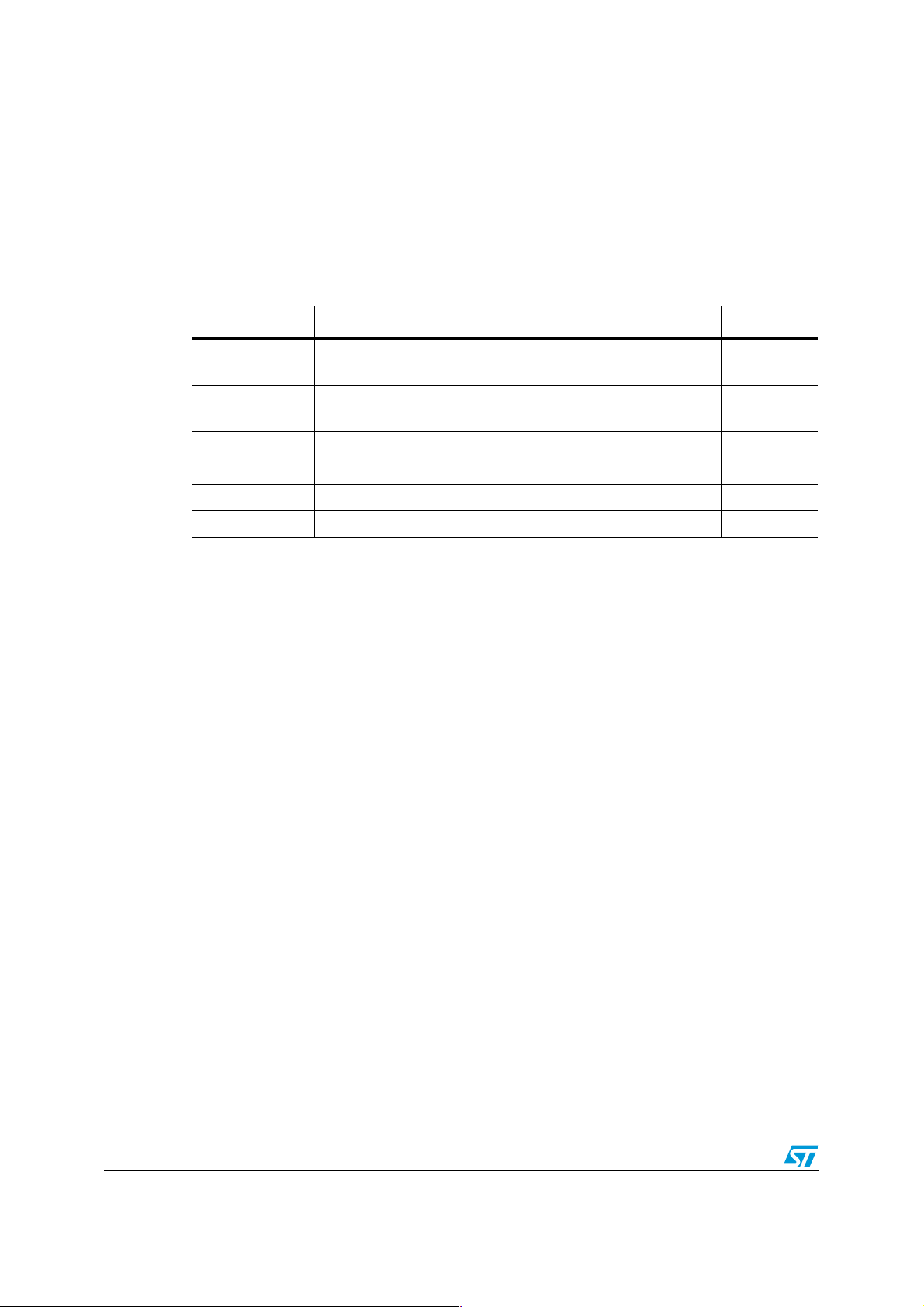
Figure 1. The STEVAL-PSQ001V1 demo board
The block diagram of the System Supply board is shown in Figure 2. There are four DC-DC
converters, two linear regulators and a reset circuit. These parts are split into five relatively
independent units: the input part, a dual DC-DC converter based on the PM6680A and
generating 2 outputs (Output 1 and Output 2), two single DC-DC converters based on the
L5970A (Output 3 and Output 4) with linear regulator, and the reset circuit.
Figure 2. Block diagram of System Supply board
Reset signal
Analog
5 V analog 500 mA
3.3 V analog 150 mA
Output 3
V
3.3 V 400 mA
sys
V
2.5 V 400 mA
aux
Output 2
V
1.0 - 3.3 V 2 A
i/o
V
voltage settings
i/o
Output 1
V
0.9 - 2.5 V 4 A
core
V
voltage settings
core
AI12693
Input
5 - 36 V
Input
protection
Skip mode
settings
PM6680A
V
core
Vi/o
E/D + start up
sequence settings
E/D analog
L5970AD
L5970AD
E/D V
FB V
FB V
sys
i/o
core
STM6719
LK112
M33
KF25
+ V
aux
5/35
Page 6
Description AN2559
2.1 Input part
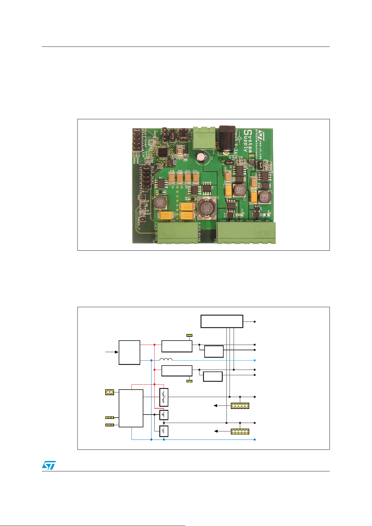
The input part shown in Figure 3 consists of the input connectors (industrial - J16 or power
jack - J3), input storage capacitor (C1) and transil (D1). The input electrolytic capacitor and
transil serve to reduce input voltage spikes (surge).
Figure 3. Schematic of input part
Vin
J16
J3
Figure 4 displays the placement of the input connectors on the board. The board can be
supplied either from the jack connector (J3) or the industrial removable terminal plate (J16).
The polarity of the input voltage must be correctly applied in accordance with the illustration
in Figure 4. If the connection is made incorrectly, the input protection D1 shorts the input
voltage. It should be pointed out that the total input current is about 4 A at maximum output
power and minimum input voltage.
1
2
3
D1
SM6T39AC147 µF / 50 V
AI12691
Figure 4. Location and correct polarity of the input supply connector on the board
-
+
+
-
+
+
6/35
Page 7
AN2559 PM6680A block
3 PM6680A block
Figure 5. Electrical diagram of the PM6680A section
core
S13
1 V
V
S14
1.2 V
S15
1.5 V
S16
1.8 V
S17
2.5 V
R206
6.8 kΩ
R205 200R
C29
330 µF /
6.3 V
C24
4.7µF / 50 V / X7R
C34 12 nF
R38 3.3 kΩ
L4 3.8 µH / 6 A
C23
R2762 kΩ
4.7µF / 50 V / X7R
Vin
SHDN
Q2
STS7NF60L
D10
4V7
51 kΩ
R29
C17
100 nF
C16
R9
3.3 Ω
Vin
VLDO
3.3 µF / 35 V
C15
470 nF
C14
4.7 µF / 10 V
C25
100nF
D7
BAW56/SOT
R37 47R
Vin
R210R
R26
23
10R
BOOT1
Vin
19
LDO5
18
CC
V
31
BOOT2
9
R25
10R
C31
220 nF
R230R
100 nF
C19
4
STS4DNF60
Q1
6
5
C18
4.7 µF / 50 V/X7R
C41
4.7 µF / 50 V/X7R
D9
STPS1L40
Q3
STS7NF60L
R220R
R19 1 kΩ
21
20
29
15
14
PGND
LGATE1
HGATE122PHASE1
CSENSE1
HGATE210PHASE211LGATE213CSENSE212V5SW17OUT28COMP22PGOOD227FB27SHDN
R240R
R10 1.8 kΩ
2
7
138
D8
STPS1L40
R40100 kΩ
L3 5.0 µH / 3 A
C35 10 nF
R39 3.3 kΩ
R110
4.7 kΩ
R105
S8
2.5 V
R109 3.3 kΩ
S12
1.8 V
S11
1.5 V
S10
1.2 V
io
S9
1 V
V
R208
820 kΩ
R201
1 kΩ
2 kΩ
9.1 kΩ
R202
R207
R203
3 kΩ
R204
3 kΩ
22 µF / 6.3 V
C40
330 µF / 6.3 V
C28
R20 680R
C27
C26 2.2 nF
OUT1
R11 560R
200R
120 pF
VLDO
R3210 kΩ
VLDO
16
26
28
30
FB1
NC
COMP1
R28 10 kΩ
VLDO
C20 1.8 nF
C22
330 µF / 6.3 V
C39
22 µF / 6.3 V
R104
R106
R103
R102
R101
6
SGND11SGND2
PGOOD1
3 kΩ
6.8 kΩ
3 kΩ
2 kΩ
1 kΩ
S7
3
FSEL
S6
SKIP
24
S5
32
VREF
EN1
25
EN2
4
5
2
3
SHDN
1
U5
PM6680
S3
VLDO
C21
91 pF
R108
820 kΩ
R107
9.1 kΩ
C30
100 nF
SKIP mode
S4
1
2
R36
51 kΩ
CH1 EN/SUS
3
R35
51 kΩ
CH2 EN/SUS
R31 10 kΩ
R3410 kΩ
AI14512
7/35
Page 8

PM6680A block AN2559
The PM6680A block is most important part of board. It contains two DC-DC converters.
Each output has a selectable output voltage level. The first converter is capable of delivering
up to 4 A for each voltage level, while the second converter can deliver up to 2 A on the
output.
Both converters are controlled by the PM6680A device. The PM6680A is a dual step-down
controller specifically designed to provide extremely high efficiency conversion, with lossless current sensing. The constant on-time architecture assures fast load transient response
and the embedded voltage feed-forward provides nearly constant switching frequency
operation. An embedded integrator control loop compensates the DC voltage error due to
the output ripple. The pulse skipping technique increases efficiency at very light loads.
Moreover, a minimum switching frequency of 33 kHz is selectable to avoid audio noise
issues. The PM6680A provides a selectable switching frequency, allowing either 200 / 300
kHz, 300 / 400 kHz or 400 / 500 kHz operation of the two switching sections. The output
voltages OUT1 and OUT2 can be adjusted from 0.9 V to 5 V and from 0.9 V to 3.3 V,
respectively. A detailed description of this device can be found in the datasheet.
Figure 5 shows the full electrical diagram of the block with the PM6680A that controls the
two DC-DC converters. The components around the PM6680A form several functional
blocks: the power management block, V
step down block, V
CORE
step down block and
I/O
start-up/enable control system block.
3.0.1 Power management block
The PM6680A has two supply voltage inputs - VCC and VIN. The VCC pin should be
connected to the 5 V bus (maximum input voltage is 6 V, minimum 4.5 V) and it is dedicated
for the supply of the chip itself. The V
it is used inside the chip for two reasons. The first is to supply the integrated LDO. The
second is the fact that the controller must sense the converter input voltage level for proper
functioning of the converter.
The V
pin is supplied from the integrated LDO (connected output of LDO and VCC) on the
CC
reference board. The V5SW feature of the LDO is disabled.
The power management block consists of components C14 - C17, C31, R9, R29, R37 and
D10. The important parts of the power management block of the device are the low pass
filters (R9, C16, C17 and R37, C31) applied to reduce the influence of transience on the
device V
and VIN main power inputs. The resistor R29 and the diode D10 generate the
CC
SHDN (shut down) signal, which is active in low level. This signal activates the PM6680A
immediately after V
is connected to the input. The V
IN
simultaneously with activation of the SHDN pin.
3.0.2 Start-up/enable block
The PM6680A has several inputs and outputs dedicated to the control of each channel.
Each channel has an independent Enable signal (EN - active in high level) and "power good"
signal (PGOOD - open collector) activated by channel in cases where the output voltage is
within 10% tolerance. These control pins can be used either for simple enabling/disabling or
for delaying the start-up of one channel rather than another.
pin should be connected to the input power bus and
IN
and LDO signals start to work
REF
The jumpers S3 and S4 with resistors R28, R31, R32, R34, R35 and R36 are used for
systems independently allowing either enabling or disabling of each channel or setting up a
different start-up sequence of both channels. Figure 6 displays the placement of jumpers S3
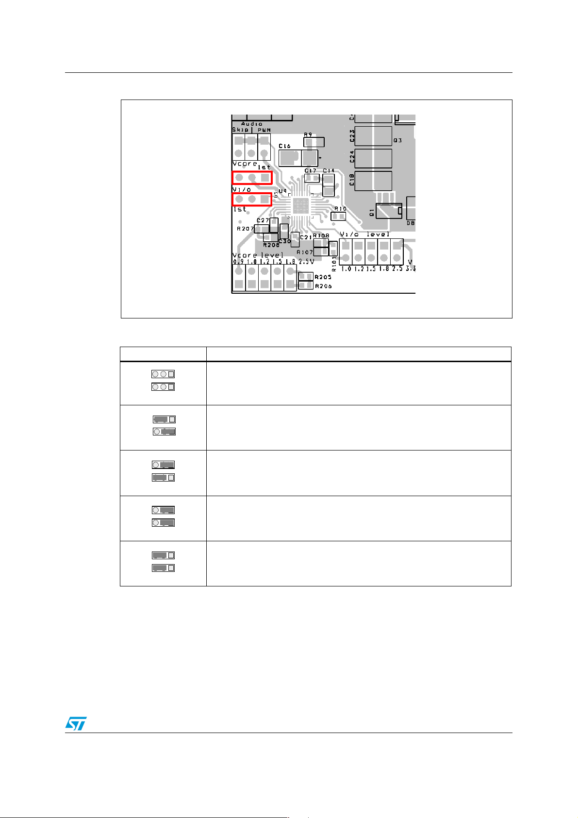
and S4 on the board, and the settings are shown in Ta b le 2 .
8/35
Page 9
AN2559 PM6680A block
V
V
V
V
V
V
V
V
V
V
V
V
Figure 6. The placement of the jumpers for start-up/enable settings
Table 2. Start-up/enable jumper settings
Jumper settings Function
Vi/o
Vi/o
1st
1st
Vi/o
Vi/o
Vi/o
Vcore
Vcore
1st
1st
Both channels are disabled. An open connector for each channel means
that the channel is disabled.
core
core
core
1st
1st
1st
Vi/o
Vi/o
Vi/o
1st
1st
1st
core
core
core
1st
1st
1st
Both channels are disabled.
Both channels are enabled and start at same time.
core
core
core
1st
1st
1st
Vi/o
Vi/o
Vi/o
core
core
core
1st
1st
1st
Vi/o
Vi/o
Vi/o
V
voltage starts first, and V
CORE
V
voltage starts first, and V
I/O
starts second.
I/O
starts second.
CORE
The Skip mode connector (shown in the schematic as S5 - S7) is dedicated for the control of
Skip mode. This connector setting is common for both channels. Figure 7 shows the
placement of the Skip mode connector, while the settings are shown in Tabl e 3 . There are
three possible settings. Standard Skip mode, No Audible mode or PWM mode. In Standard
Skip mode the converter reduces the switching frequency at light load to maintain good
efficiency even in this condition. There is no lower limit for switching frequency. In No
Audible mode the converter reduces switching frequency at light load, but this frequency
never drops below 30 kHz to avoid possible audible noise caused by the mechanical
9/35
Page 10
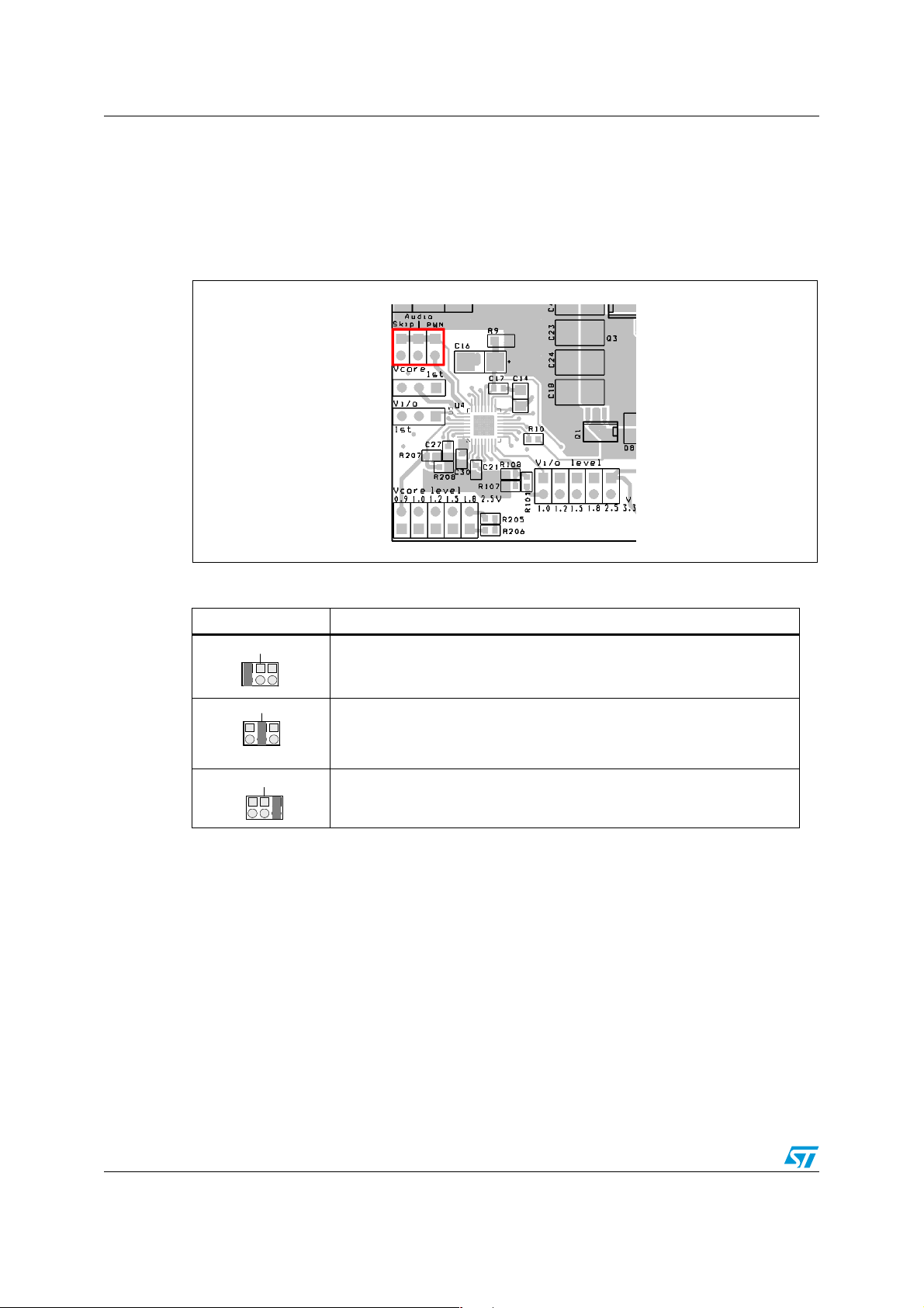
PM6680A block AN2559
construction of passive components (inductors or ceramic capacitors). In PWM mode the
converter maintains a constant switching frequency independently on the load.
The FSEL pin the PM6680A dedicated for operating frequency setting is connected to GND.
This means that the switching frequency of the V
frequency of V
is 300 kHz.
I/O
branch is 200 kHz and switching
CORE
Figure 7. Skip mode connector
Table 3. Skip mode connector jumper settings
Jumper settings Function
Audio
Audio
Audio
Skip PWM
Skip PWM
Skip PWM
Audio
Audio
Audio
Skip PWM
Skip PWM
Skip PWM
Audio
Audio
Audio
Skip PWM
Skip PWM
Skip PWM
3.0.3 Step-down parts
The PM6680A is a dual step-down controller and drives two step-down converters. The
schematic of both channels are almost identical, with only a few small differences. Since
each channel is for a different output power, the main difference is in the components’
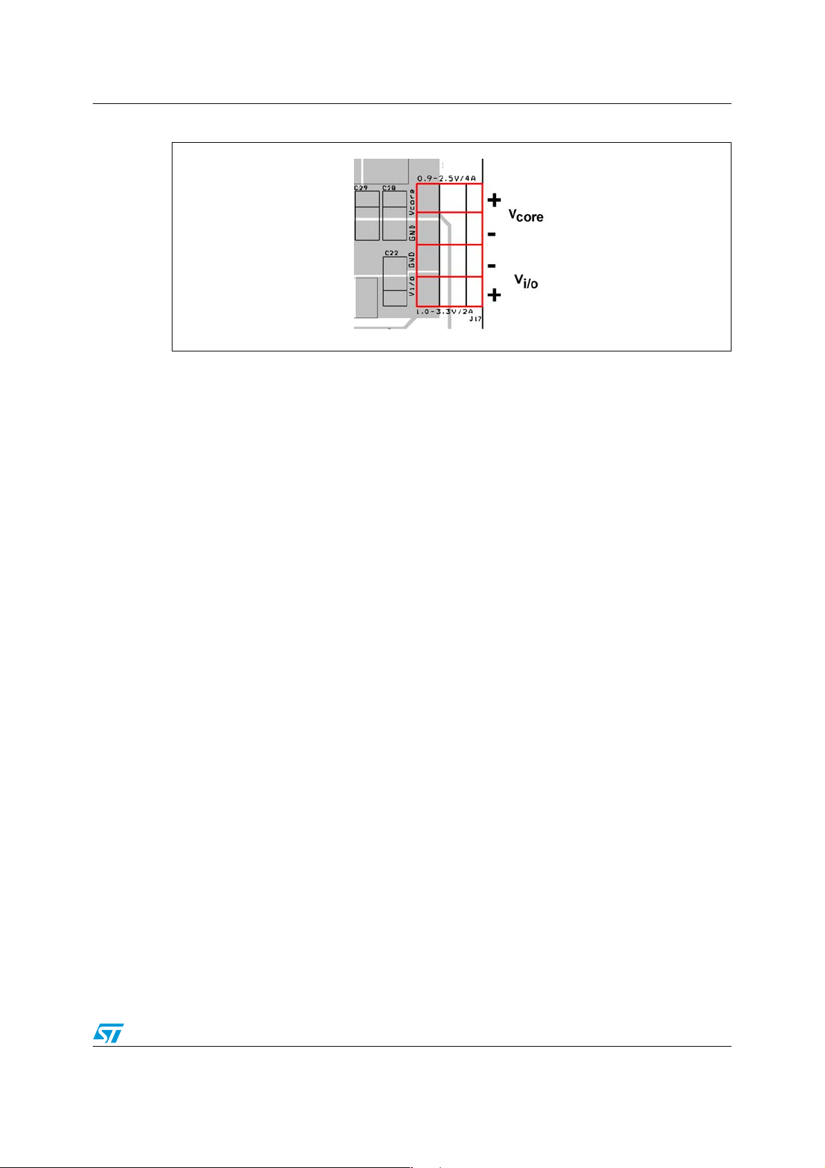
values. Figure 8 displays the output connector polarities of the PM6680A section.
Skip mode at light load.
No Audible Skip mode at light load (frequency never drops below 30 kHz).
PWM mode. Constant frequency even at light or zero load.
10/35
Page 11
AN2559 PM6680A block
Figure 8. Output connector
The power components of the step-down part are input capacitors (C23, C24 or C18, C41),
the half bridge driver containing two N-channel MOSFETs (Q2, Q3 or Q1), inductors (L4 or
L3) and output capacitors (C28, C29, C40 or C22, C39).
Ceramic high-capacitance capacitors are used as input capacitors. 60 V MOSFETs are
used for the half bridge driver. A relatively high breakdown voltage is used to guarantee
operation in industrial applications. Because the V
output is designed for lower currents
I/O
(2 A), both MOSFETs are integrated in one SO-8 package (Q1 - STS4NF60). This helps to
reduce the size on the PCB. Two discrete MOSFETs (STS7NF60) are used for the V
CORE
higher power output (4 A). Schottky diodes are also used in each channel (D9 or D8). These
diodes work mainly during dead time and are not mandatory for proper functioning, but their
application increases efficiency.
The 5 µH inductor (L3) is used for the V
output with saturation current at 3 A. The inductor
I/O
L4 has value of 3.8 µH with saturation current at 6 A.
A combination of tantalum low ESR and ceramic type are used as output capacitors.
Ceramic capacitors help to reduce total output ESR and reduce total output voltage ripple.
The PM6680A includes a half bridge driver for each channel. The external bootstrap diode
and capacitor must be applied (D7, C19 or C25) in order to drive the gates of the high side
MOSFETs.
The feedback signal is generated by the output voltage divider (R10x or R20x). The board
allows the setting of different output voltages for both channels. Figure 9 and Figure 10
display the output voltage connector placement on the board for each channel. The jumper
settings are shown in Tabl e 4 and Tab l e 5, respectively.
In classic Constant On Time control, the system regulates the valley value of the output
voltage and not the average value. In this condition, the output voltage ripple is a source of
DC static error. To compensate for this error, an integrator network is introduced in the
control loop by connecting the signal output voltage to the COMP1/COMP2 pin through a
capacitor (C20 or C26). An additional R-C network (R11 and C21 or R20 and C27) is
implemented as a low pass filter to reduce noise on the input of the COMP pin.
Since the feedback signal of the SMPS working in Constant On Time control is directly
connected to the PWM comparator, the stability of the SMPS is more sensitive to noise
injected into the FB signal. It is possible to attenuate the affect of the noise to stabilize the
SMPS by implementing the so called "Virtual ESR" network, which increases the amplitude
of the feedback ripple voltage and improves signal-to-noise ratio. The Virtual ESR network
does not increase the output ripple voltage. It is recommended to use the Virtual ESR
network in cases where the output voltage ripple is below 30 mV. However, it is necessary to
11/35
Page 12

PM6680A block AN2559
take into consideration that the influence of noise on the performance of the SMPS strictly
depends on the PCB layout. Therefore, the 30 mV is an indicative value. Virtual ESR
Networks are applied for each channel on the reference board described in this application
note. The main reason for this is the fact that the SMPS based on the PM6680A device can
generate different output voltages at a wide input voltage range. As output voltage ripple
depends also on input and output voltage level, there are configurations where the Virtual
ESR network could be mandatory. Virtual ESR networks consists of R40, R39, C35 or R27,
R38 or C34. The ESR network can be removed to observe influence of ESR network to
board function. To remove the Virtual ESR Network, R40 and R27 must be removed and
R39 and R38, respectively, must be shorted.
Figure 9. Jumper placement for V
Table 4. V
voltage level jumper settings
CORE
Jumper settings V
voltage level setting
CORE
CORE
2.5 V
1.8 V
1.5 V
1.2 V
1.0 V
0.9 V
12/35
Page 13

AN2559 PM6680A block
Figure 10. Jumper placement for V
Table 5. V
voltage level jumper settings
I/O
Jumper settings V
voltage level setting
I/O
CORE
3.3 V
2.5 V
1.8 V
1.5 V
1.2 V
1.0 V
13/35
Page 14

PM6680A block AN2559
3.1 DC-DC converters based on the L5970AD
There are two converters based on the L5970AD on the System Supply board: the analog
output and V
connector J18.
Figure 11. Output voltages of L5970A parts
output voltage. Figure 11 shows the arrangement of output voltages on
SYS
The L5970AD is a step-down monolithic power switching regulator with a switch current limit
of 1.5 A, capable of delivering more than 1 A of DC current to the load depending on the
application conditions. The output voltage can be set from 1.235 V to 35 V. The device uses
an internal P-channel D-MOS transistor (with a typical RDS
of 200 mΩ) as a switching
ON
element to avoid the use of a bootstrap capacitor and to guarantee high efficiency. An
internal oscillator fixes the switching frequency at 500 kHz to minimize the size of external
components. Having a minimum input voltage of only 4.4 V, it is particularly suitable for 5 V
buses, found in all computer-related applications. Pulse-by-pulse current limiting with
internal frequency modulation offers effective constant current short circuit protection.
The schematic of both SMPS’s is displayed in Figure 12. As the schematic shows, designing
with the L5970AD is very simple. It consists of a power part, feedback and enable/disable
connectors. The power part contains an input capacitor (C2 or C8 - ceramic is
recommended), an inductor (L1 or L2), an output capacitor (C5 or C11) and a freewheeling
diode (D4 or D6). The feedback part consists of a voltage divider (R2, R3, R4 or R6, R7, R8)
and a compensation RC network (R1, C3, C4 or R5, C9, C10).
14/35
Page 15

AN2559 PM6680A block
Figure 12. Schematic of the two SMPS’s based on the L5970AD
sys
aux
V
V5A
V3A3
4
OUT
LK112_33
SHDN1GND2BYPASS
IN
U2
5
R3
20 kΩ
R2
120 kΩ
33 µH / 1. 5 A
L1
1
5
FB
INH
OUT
GND
REF
V
CC
U1 L5970AD
V
COMP
8
SYNC
4
R1
3
C7
10 µF / 6 V
C5
R4
D4
3
7
6
2
4.7 kΩ
GNDA
C6
100 nF
47 µF / 10 V
5.6 kΩ
Vin
R4 1 51 kΩ
STPS2L40
EN
analog
V
S1
C4
22 nF
V
C13
10 µF / 4 V
1
GND
VOUT
7
6
GND
3
GND
2
GND
VIN
INH
U4 KF25_SOI C8
8
5
C12
100 nF
R7
240 kΩ
C11
100 µF / 6 V
R6
18 kΩ
R8
10 kΩ
L2 3 3 µH / 1.5 A
1
OUT
CC
U3 L5970AD
V
8
4
D6
5
FB
COMP
STPS2L40
INH
3
7
GND
6
REF
V
2
SYNC
C10
22 nF
4.7 kΩ
R5
AI12694
Vin
R4 2 51 kΩ
EN
sys
S2 V
C3
220 pF
C2
4.7 µF / 5 0 V
L5 10 µH / 1 A
Vin
C9
220pF
4.7 µF / 5 0 V
C8
Both converters can be switched on or off using the inhibit pin of L5970AD connected to
jumpers S1 and S2. If the jumper is left open, the DC-DC converter will not operate. Thus
the jumper must be shorted for the converter to operate (see Figure 13 for board placement
of the jumper and Tab l e 6 for the jumper settings).
15/35
Page 16

PM6680A block AN2559
Figure 13. Jumper placement for enable/disable function of analog output and
output3
Table 6. Jumper settings for enable/disable function of analog output and output3
Jumper settings V
E/DE/D
CORE
Analog disable
There is an LDO linear regulator (U2 and U4) on the output of each DC-DC converter. The
LK112_33 is a 3.3 V linear regulator in a SOT23-5 package. The KF25 is a very low dropout
regulator with an output voltage of 2.5 V and output current of up to 400 mA.
3.2 Reset circuit
The board also features a reset circuit which supervises the output voltages. It is based on
the STM6719 series of low voltage / low supply supervisors, which are designed to monitor
three system power supply voltages. Two monitored supplies (V
(factory trimmed) thresholds (V
externally adjustable RSTIN threshold (0.626 V internal reference). If any of the three
monitored voltages drop below its factory-trimmed or adjustable thresholds, or if MR is
asserted to logic low, an RST is asserted (driven low). Once asserted, RST is maintained at
Low for a minimum delay period after ALL supplies rise above their respective thresholds
and MR returns to High. This device is guaranteed to be in the correct reset output logic
state when V
pin SOT23 package.
and / or V
CC1
E/DE/D
E/DE/DE/D
E/DE/DE/D
Analog enable
Output3 disable
Output3 enable
and V
and V
RST1
is greater than 0.8 V. This device is available in a standard 6-
CC2
). The third voltage is monitored using an
RST2
CC1
) have fixed
CC2
16/35
Page 17

AN2559 PM6680A block
Figure 14 shows the schematic and placement of the reset part on the board. Typically in
real applications the reset circuit senses if the supply voltage drops below about 10% of
nominal value. This feature cannot be implemented on the System Supply board due to the
fact that the output voltage is selectable, while the reset voltage is factory set. There are
several types of reset circuits in the STM6719 family (see datasheet). Of these, the
STM6719TGWB6F was selected as optimal. The voltage thresholds of this device are
3.075 V, 1.11 V and 0.626 V.
Figure 14. Schematic of the reset circuit and board placement
V
sys
V
V
io
core
C32
1 nF
U6
STM6719TEWB6F
6
V
4
V
5
RSTIN
3
MR
C33
1 nF
CC1
CC2
RST
V
SS
2
R209
110 kΩ
1
J14 Reset
J15 Reset GND
AI12695
17/35
Page 18

PCB layout AN2559
4 PCB layout
The System Supply board utilizes a four-layer PCB. The copper layout of each layer is
shown in Figure 15 and Figure 16. The top and bottom layers show also the placement of
the components. To reduce the size of board while maintaining the ability to change some
components, size 0603 was used for the majority of the passive components. All views of
the PCB are from top side.
Figure 15. PCB top layer layout and first internal layer
Figure 16. PCB second internal layer and bottom layer layout
18/35
Page 19

AN2559 Bill of materials
5 Bill of materials
Table 7. Bill of materials
Item Part Description Type Size Manufacturer Part number
1 C1 47 µF / 50 V TH 6.3 x 11 E47M/50VMXA RM5
2 C2 4.7 µF / 50 V SMD 1812 AVX 18125C475KAT2A
3 C3 220 pF SMD 0603
4 C4 22 nF SMD 0603
5 C5 100 µF / 10 V SMD C AVX TPSC107M010X0150
6C6 N.A.
7 C7 10 µF / 6 V SMD B CTS 10M / 6.3 V
8 C8 4.7 µF / 50 V SMD 1812 AVX 18125C475KAT2A
9 C9 220 pF SMD 0603
10 C10 22 nF SMD 0603
11 C11 100 µF / 10 V SMD C AVX TPSC107M010X0150
12 C12 100 nF SMD 0805
13 C13 10 µF / 6.3 V SMD B CTS 10 M / 6.3 V
14 C14 6.8 µF / 10 V SMD B CTS 6 M 8 / 10 V
15 C15 470 nF SMD 0805
16 C16 3.3 µF / 50 V SMD 1812 C1210C335K5RAC
17 C17 100 nF SMD 0603
18 C18 4.7 µF / 50 V / X7R SMD 1812 AVX 18125C475KAT2A
19 C19 100 nF SMD 0603
20 C20 1.8 nF SMD 0603
21 C21 100 pF SMD 0603
22 C22 330 µF / 6.3 V SMD D AVX TPSD337M006X0045
23 C23 4.7 µF / 50 V / X7R SMD 1812 AVX 18125C475KAT2A
24 C24 4.7 µF / 50 V / X7R SMD 1812 AVX 18125C475KAT2A
25 C25 100 nF SMD 0603
26 C26 2.2 nF SMD 0603
27 C27 120 pF SMD 0603
28 C28 330 µF / 6.3 V / 45 mΩ SMD D AVX TPSD337M006X0045
29 C29 330 µF / 6.3 V / 45 mΩ SMD D AVX TPSD337M006X0045
30 C30 100 nF SMD 0603
31 C31 220 nF SMD 0805
32 C32 1 nF SMD 0603
19/35
Page 20

Bill of materials AN2559
Table 7. Bill of materials (continued)
Item Part Description Type Size Manufacturer Part number
33 C33 1 nF SMD 0603
34 C34 12 nF SMD 0603
35 C35 10 nF SMD 0603
36 C39 22 µF / 6.3 V SMD 1206 AVX 12066D226KAT2A
37 C40 100 µF / 6.3 V SMD 1210 AVX 12104D107MAT2A
38 C41 4 µF 7 / 50 V / X7R SMD 1812 AVX 18125C475KAT2A
39 D1 SM6T39A SMD SMB ST SMA6T39A
40 D4 STPS2L40 SMD SMB ST STPS2L40
41 D6 STPS2L40 SMD SMB ST STPS2L40
42 D7 BAW56/SOT SMD SOT23
43 D8 STPS1L40M SMD DO216-AA ST STPS1L40M
44 D9 STPS1L40M SMD DO216-AA ST STPS1L40M
45 D10 4.7 V SMD SOD80
46 S1 Header 1 x 2 TH
47 S2 Header 1 x 2 TH
48 S3 Header 1 x 3 TH
49 S4 Header 1 x 3 TH
50 V
51 V
level Header 2 x 5 TH
I/O
level Header 2 x 5 TH
CORE
52 Skip Header 2 x 3 TH
53 J3 Jack - PCB TH
54 J14 Header 1 x 1 TH
55 J15 Header 1 x 1 TH
56 J16 Ind. Con. 2 TH Ph. Con. MSTBA 2,5 / 2-G-5,08
57 J17 Ind. Con. 4 TH Ph. Con. MSTBA 2,5 / 4-G-5,08
58 J18 Ind. Con. 6 TH Ph. Con MSTBA 2,5 / 6-G-5,08
59 L1 33 µH / 1.5 A SMD Coilcraft MSS7341-333MLB
60 L2 33 µH / 1.5 A SMD Coilcraft MSS7341-333MLB
61 L3 5.0 µH / 3 A SMD Coilcraft MSS7341-502MLB
62 L4 3.8 µH / 6 A SMD Coilcraft MSS1038-382NLB
63 L5 1 µH / 1 A SMD Coilcraft ME3220-102MLB
64 Q1 STS4DNF60 SMD ST STS4DNF60L
65 Q2 STS7NF60L SMD ST STS7NF60L
66 Q3 STS7NF60L SMD ST STS7NF60L
67 R1 4. 7 kΩ SMD 0603
20/35
Page 21

AN2559 Bill of materials
Table 7. Bill of materials (continued)
Item Part Description Type Size Manufacturer Part number
68 R2 36 kΩ / 1% SMD 0603
69 R3 200 kΩ/ 1% SMD 0603
70 R4 10 kΩ / 1% SMD 0603
71 R5 4.7 kΩ SMD 0603
72 R6 18 kΩ / 1% SMD 0603
73 R7 240 kΩ / 1% SMD 0603
74 R8 10 kΩ / 1% SMD 0603
75 R9 3.3 Ω SMD 0805
76 R10 1.8 kΩ SMD 0603
77 R11 560 Ω SMD 0603
78 R110 4.7 kΩ / 1% SMD 0603
79 R19 1 kΩ SMD 0603
80 R20 680 Ω SMD 0603
81 R21 0 Ω SMD 0603
82 R22 0 Ω SMD 0603
83 R23 0 Ω SMD 0603
84 R24 0 Ω SMD 0603
85 R25 10 Ω SMD 0603
86 R26 10 Ω SMD 0603
87 R27 62 kΩ SMD 0603
88 R28 10 kΩ SMD 0603
89 R29 51 kΩ SMD 0603
90 R31 10 kΩ SMD 0603
91 R32 10 kΩ SMD 0603
92 R34 10 kΩ SMD 0603
93 R35 51 kΩ SMD 0603
94 R36 51 kΩ SMD 0603
95 R37 47 Ω SMD 0603
96 R38 3.3 kΩ SMD 0603
97 R39 3.3 kΩ SMD 0603
98 R40 100 kΩ SMD 0603
99 R41 51 kΩ SMD 0603
100 R42 51 kΩ SMD 0603
101 R101 1 k
102 R102 2 kΩ / 1% SMD 0603
Ω / 1% SMD 0603
21/35
Page 22

Bill of materials AN2559
Table 7. Bill of materials (continued)
Item Part Description Type Size Manufacturer Part number
103 R103 3 kΩ / 1% SMD 0603
104 R104 3 kΩ / 1% SMD 0603
105 R105 200 Ω / 1% SMD 0603
106 R106 6.8 kΩ / 1% SMD 0603
107 R107 9.1 kΩ / 1% SMD 0603
108 R108 820 kΩ / 1% SMD 0603
109 R109 3.3 kΩ / 1% SMD 0603
110 R201 1 kΩ / 1% SMD 0603
111 R202 2 kΩ / 1% SMD 0603
112 R203 3 kΩ / 1% SMD 0603
113 R204 3 kΩ / 1% SMD 0603
114 R205 200 Ω / 1% SMD 0603
115 R206 6.8 kΩ / 1% SMD 0603
116 R207 9.1 kΩ / 1% SMD 0603
117 R208 820 kΩ / 1% SMD 0603
118 R209 51 kΩ SMD 0603
119 U1 L5970AD SMD SO-8 ST L5970AD
120 U2 LK112_33 SMD SOT23-5 ST LK112M33TR
121 U3 L5970AD SMD SO-8 ST L5970AD
122 U4 KF25_SOIC8 SMD SO-8 ST KF25BD-TR
123 U5 PM6680A SMD
124 U6 STM6719TEWB6F SMD SOT23-6 ST STM6719TGWB6F
VFQFPN-
32 5X5
ST PM6680A
22/35
Page 23

AN2559 Measurements
6 Measurements
The performance and properties of each part of the board is indicated in the measurements
below. These measurements were performed for the PM6680A and L5971AD blocks
independently.
6.1 PM6680A block - measurements
The performance measurements of the PM6680A part focus mainly on efficiency, light load
consumption, output ripple and transients.
6.1.1 Efficiency and light load consumption modes
Since the device consists of three power parts (two controllers and one LDO) it makes
sense to measure total efficiency. Figure 17 displays how efficiency depends on input
voltage level at full load output (V
Figure 17. Efficiency of the dual step-down converter at full load
Efficency (%)
2.5 V / 4 A, V
CORE
3.3 V / 2 A).
I/O
100.0
90.0
80.0
70.0
60.0
50.0
40.0
30.0
20.0
10.0
0.0
0 5 10 15 20 25 30 35 40
Vin (V)
AI12696
The efficiency is in the range of 83 - 91%. It should be noted that the total efficiency strictly
depends on the performance of each component. The System Supply board was designed
to satisfy a wide input voltage range. Therefore, 60 V MOSFETS are used on the board. If
the input voltage of the end application is less (up to 30 V for instance), efficiency can be
improved by using lower RDS
30 V MOSFETs in the same package. The expected
ON
efficiency gain is about 3 - 4%.
The PM6680A can work in several modes with regard to light load. These options are mainly
used for battery applications where relatively high consumption at light load can drain the
battery even when no power is requested. The PM6680A allows three modes (see 3.0.2):
PWM, No Audible Noise and Skip. Figure 18 shows the consumption of the board for
different modes of the PM6680A. There is no load on the output and other parts of the
SMPS are disabled.
23/35
Page 24

Measurements AN2559
Figure 18. PM6680A consumption at no load condition, in the different modes
lin (mA)
70.0
60.0
50.0
40.0
30.0
20.0
10.0
0.0
0 5 10 15 20 25 30 35 40
PWM
No Audible
SKIP
Vin (V)
In analyzing the data in Figure 18, it should be noted that the consumption is slightly
increased by several passive components which generate inhibit of the L5970ADs. Total
consumption of these parts at 35 V on the input is about 1.5 mA. This is not compensated
for in the chart in Figure 18. It is possible to see the effect of the different operating modes of
the converter by observing the output ripple voltage waveforms in Figure 19. These
measurements are made under the following conditions: V
output set to 2.5 V, no load,
CORE
at 12 V on the input.
Figure 19. Output voltage ripple in different modes of light load operation
AI12697
6.1.2 Output voltage ripple
Output voltage ripple depends on the current ripple flowing through the choke. The current
ripple depends on the input and output voltage levels. Therefore, it is mandatory to measure
the output voltage ripple for different input and output voltage conditions. Figure 20 shows
the output voltage ripple of V
displays the output voltage ripple of V
shows the output voltage ripple of V
displays the output voltage ripple of V
figures represent the minimum and maximum output voltages at maximum load (0.9 V and
2.5 V at 4 A for V
24/35
and 1 V and 3.3 V at 2 A for V
CORE,
at the minimum input voltage (5 V), while Figure 21
CORE
CORE
I/O
I/O
at the maximum output voltage (36 V). Figure 22
at the minimum input voltage (5 V), and Figure 20
at the maximum input voltage (36 V). All of the
).
I/O
Page 25

AN2559 Measurements
Figure 20. Output voltage ripple of V
Figure 21. Output voltage ripple of V
at the minimum input voltage (5 V)
CORE
at the maximum output voltage (36 V)
CORE
Figure 22. Output voltage ripple of V
at the minimum input voltage (5 V)
I/O
25/35
Page 26

Measurements AN2559
Figure 23. Output voltage ripple of V
at the maximum input voltage (36 V)
I/O
Figure 24. Start-up without setting the sequence
Figure 25. Start-up with a set sequence
26/35
Page 27

AN2559 Measurements
6.1.3 Start-up sequence
The correct start-up sequence of the supply voltage is typically requested by the FPGA
device. Therefore, there it is possible to set a dedicated start-up sequence on the System
Supply board (see 3.0.2. Figure 24) shows the start-up sequence waveform of V
V
outputs when the jumpers described in Tab l e 2 are set in accordance with line 3 in the
I/O
CORE
and
table.
The waveforms shown in Figure 25 illustrate different start-up sequences in accordance with
the jumper settings displayed in Tabl e 2 , lines 4 and 5.
6.1.4 Transient response
Transient response refers to the behavior of the output voltage when the load changes fast.
This test was also performed on the outputs of the PM6680A branch. The load was changed
between maximum and zero load (0 ↔ 2 A on V
output). The input voltage was 12 V and output voltage was 3.3 V and 2.5 V, respectively.
The repetition of load change was 500 Hz. The results of the measurements are shown in
Figure 26 and Figure 27. The voltage spikes caused by increasing the load are quite low. It
is possible to observe that the converter reacts very fast to a rising load and the
undervoltage is small (left waveform in figures). If the load is decreasing fast the overvoltage
spikes appear on the output (right side of picture). This effect depends partly on the reaction
of the controller and partly on the parameters of the output filter. There is remaining energy
stored in the inductor and if the load decreases this energy should be stored in the output
capacitor. This effect can be reduced by either reducing the value of the inductor (to reduce
the amount of energy stored in the inductor), or by increasing the value of the output
capacitor (a higher capacitance is capable of absorbing more energy from the inductor).
output and 0 ↔ 4 A on the V
I/O
CORE
Figure 26. Load transient response on V
CORE
output
27/35
Page 28

Measurements AN2559
Figure 27. Load transient response on V
output
I/O
28/35
Page 29

AN2559 Measurements
6.2 L5970AD blocks - measurements
6.2.1 Efficiency
The L5970AD is a powerful converter with very good performance and efficiency. Because a
diode is used as a low side switch, however, the efficiency is a slightly less compared to a
synchronous converter such as the PM6680A. Theoretically, the efficiency declines when
output voltage is decreasing and input voltage is increasing. Figure 28 displays the
efficiency of Output 3, depending on the input voltage at full load (800 mA). Figure 29
displays the same measurement for the Analog output. The efficiency of the Analog output
is better thanks to the higher output voltage level. The efficiency of the Analog output
voltage was measured in a range of 7 - 35 V. It should be noted that the output voltage is
5 V, so the device does not work as a switching converter in cases where the input and
output voltage are similar or lower than the required output. In this case the L5973AD works
with 100% duty cycle.
Figure 28. Efficiency of output 3, by input voltage level
Efficency (%)
90.0
80.0
70.0
60.0
50.0
40.0
30.0
20.0
10.0
0.0
0 5 10 15 20 25 30 35 40
Vin (V)
AI12698
29/35
Page 30

Measurements AN2559
Figure 29. Efficiency of analog output, by input voltage level
Efficency (%)
100.0
90.0
80.0
70.0
60.0
50.0
40.0
30.0
20.0
10.0
0.0
0 5 10 15 20 25 30 35 40
Vin (V)
AI14500
6.2.2 Output voltage ripple
The output voltage ripple of the switching parts of the Analog and V
Figure 30 and Figure 31. The measurements were made for different input voltages,
because the current ripple influence on the output voltage ripple depends on the input
voltage level. The output voltage ripple on the 3.3 V Analog output and the V
displayed in Figure 32 and Figure 33. As these outputs are generated by LDOs, the output
voltage ripple is the same (independent) for all input voltages, and is very low. Therefore,
only one output voltage ripple image is shown in the figures 32 and 33. All of the
measurements were taken at full output load.
Figure 30. Analog 5 V - output voltage ripple
outputs are shown in
SYS
output are
AUX
30/35
Page 31

AN2559 Measurements
Figure 31. V
- output voltage ripple
SYS
Figure 32. Analog 3.3 V - output voltage ripple
31/35
Page 32

Measurements AN2559
Figure 33. V
2.5 V - output voltage ripple
AUX
32/35
Page 33

AN2559 Measurements
6.2.3 Transient
Transient responses were measured only for V
displayed in Figure 34 and Figure 35. The transient waveforms of the L5970AD section
show the response time. The most visible difference between the L5970AD in classic
voltage mode and the PM6680A working in Constant On Time mode is the reaction when
there is a fast load increase. Whereas the PM6680A reacts asfast as possible on the rising
load, the L5970AD will wait short time as the compensation network is implemented in
feedback loop (see Figure 24 and Figure 25).
Figure 34. Transient response of V
based on the L5970AD
SYS
AUX
and V
. The transient responses are
SYS
Figure 35. Transient response of V
generated by the LDO KF25
AUX
33/35
Page 34

References AN2559
7 References
1. Datasheet PM6680A
2. Datasheet L5970AD
3. Datasheet LK112
4. Datasheet KF25
5. STM6719
6. AN1330 - designing with the L5970D, 1 A high efficiency DC-DC converter.
8 Revision history
Table 8. Document revision history
Date Revision Changes
25-Sep-2007 1 Initial release
34/35
Page 35

AN2559
Please Read Carefully:
Information in this document is provided solely in connection with ST products. STMicroelectronics NV and its subsidiaries (“ST”) reserve the
right to make changes, corrections, modifications or improvements, to this document, and the products and services described herein at any
time, without notice.
All ST products are sold pursuant to ST’s terms and conditions of sale.
Purchasers are solely responsible for the choice, selection and use of the ST products and services described herein, and ST assumes no
liability whatsoever relating to the choice, selection or use of the ST products and services described herein.
No license, express or implied, by estoppel or otherwise, to any intellectual property rights is granted under this document. If any part of this
document refers to any third party products or services it shall not be deemed a license grant by ST for the use of such third party products
or services, or any intellectual property contained therein or considered as a warranty covering the use in any manner whatsoever of such
third party products or services or any intellectual property contained therein.
UNLESS OTHERWISE SET FORTH IN ST’S TERMS AND CONDITIONS OF SALE ST DISCLAIMS ANY EXPRESS OR IMPLIED
WARRANTY WITH RESPECT TO THE USE AND/OR SALE OF ST PRODUCTS INCLUDING WITHOUT LIMITATION IMPLIED
WARRANTIES OF MERCHANTABILITY, FITNESS FOR A PARTICULAR PURPOSE (AND THEIR EQUIVALENTS UNDER THE LAWS
OF ANY JURISDICTION), OR INFRINGEMENT OF ANY PATENT, COPYRIGHT OR OTHER INTELLECTUAL PROPERTY RIGHT.
UNLESS EXPRESSLY APPROVED IN WRITING BY AN AUTHORIZED ST REPRESENTATIVE, ST PRODUCTS ARE NOT
RECOMMENDED, AUTHORIZED OR WARRANTED FOR USE IN MILITARY, AIR CRAFT, SPACE, LIFE SAVING, OR LIFE SUSTAINING
APPLICATIONS, NOR IN PRODUCTS OR SYSTEMS WHERE FAILURE OR MALFUNCTION MAY RESULT IN PERSONAL INJURY,
DEATH, OR SEVERE PROPERTY OR ENVIRONMENTAL DAMAGE. ST PRODUCTS WHICH ARE NOT SPECIFIED AS "AUTOMOTIVE
GRADE" MAY ONLY BE USED IN AUTOMOTIVE APPLICATIONS AT USER’S OWN RISK.
Resale of ST products with provisions different from the statements and/or technical features set forth in this document shall immediately void
any warranty granted by ST for the ST product or service described herein and shall not create or extend in any manner whatsoever, any
liability of ST.
ST and the ST logo are trademarks or registered trademarks of ST in various countries.
Information in this document supersedes and replaces all information previously supplied.
The ST logo is a registered trademark of STMicroelectronics. All other names are the property of their respective owners.
© 2007 STMicroelectronics - All rights reserved
STMicroelectronics group of companies
Australia - Belgium - Brazil - Canada - China - Czech Republic - Finland - France - Germany - Hong Kong - India - Israel - Italy - Japan -
Malaysia - Malta - Morocco - Singapore - Spain - Sweden - Switzerland - United Kingdom - United States of America
www.st.com
35/35
 Loading...