


AN2555
Application note
Porting an application from the ST10F269Zx to the ST10F276Z5
Introduction
The ST10F276Z5 is a member of the STMicroelectronics ST10 family of 16-bit single-chip
CMOS microcontrollers. It is functionally upward compatible with the ST10F269Zx.
The goal of this document is to highlight the differences between ST10F269Zx and
ST10F276Z5 devices. It is intended for hardware or software designers who are adapting an
existing application based on the ST10F269Zx to the ST10F276Z5.
This document presents the ST10F276Z5’s modified functionalities and the new ones then it
describes the modified registers and the new registers. For each part, the differences with
the ST10F269Zx that may have an impact when replacing the ST10F269Zx by the
ST10F276Z5 are stressed and some advice is given on the way they can be handled.
This document applies from the second silicon version of the ST10F276Z5, that is from the
BA step where a new sectorization of the Flash memory was introduced. The silicon version
can be verified by reading the IDCHIP register at location 00’F07Ch. The values for these
silicon versions are 114Xh with X > 1.
July 2007 Rev 1 1/33
www.st.com

AN2555 - Application note Contents
Contents
1 Modified features . . . . . . . . . . . . . . . . . . . . . . . . . . . . . . . . . . . . . . . . . . . . 3
1.1 Pinout . . . . . . . . . . . . . . . . . . . . . . . . . . . . . . . . . . . . . . . . . . . . . . . . . . . . . . . . . 3
1.2 XRAM . . . . . . . . . . . . . . . . . . . . . . . . . . . . . . . . . . . . . . . . . . . . . . . . . . . . . . . . . 5
1.3 Flash EEPROM . . . . . . . . . . . . . . . . . . . . . . . . . . . . . . . . . . . . . . . . . . . . . . . . . . 6
1.4 A/D converter . . . . . . . . . . . . . . . . . . . . . . . . . . . . . . . . . . . . . . . . . . . . . . . . . . . . 7
1.5 Real Time Clock . . . . . . . . . . . . . . . . . . . . . . . . . . . . . . . . . . . . . . . . . . . . . . . . 12
1.6 CAN modules . . . . . . . . . . . . . . . . . . . . . . . . . . . . . . . . . . . . . . . . . . . . . . . . . . 13
1.7 Port input control . . . . . . . . . . . . . . . . . . . . . . . . . . . . . . . . . . . . . . . . . . . . . . . . 14
1.8 Port output control . . . . . . . . . . . . . . . . . . . . . . . . . . . . . . . . . . . . . . . . . . . . . . . 15
1.9 PLL and main on-chip oscillator . . . . . . . . . . . . . . . . . . . . . . . . . . . . . . . . . . . . 16
2 New features . . . . . . . . . . . . . . . . . . . . . . . . . . . . . . . . . . . . . . . . . . . . . . 18
2.1 Additional XPeripherals . . . . . . . . . . . . . . . . . . . . . . . . . . . . . . . . . . . . . . . . . . . 18
2.2 New multiplexer for X-Interrupts . . . . . . . . . . . . . . . . . . . . . . . . . . . . . . . . . . . . 18
2.3 Programmable divider on CLKOUT . . . . . . . . . . . . . . . . . . . . . . . . . . . . . . . . . . 20
2.4 Additional port input control: XPICON register . . . . . . . . . . . . . . . . . . . . . . . . . 21
3 Modified registers . . . . . . . . . . . . . . . . . . . . . . . . . . . . . . . . . . . . . . . . . . 22
3.1 XPERCON register . . . . . . . . . . . . . . . . . . . . . . . . . . . . . . . . . . . . . . . . . . . . . . 22
3.2 IDCHIP register . . . . . . . . . . . . . . . . . . . . . . . . . . . . . . . . . . . . . . . . . . . . . . . . . 23
4 New registers . . . . . . . . . . . . . . . . . . . . . . . . . . . . . . . . . . . . . . . . . . . . . . 25
4.1 XADRS3 register . . . . . . . . . . . . . . . . . . . . . . . . . . . . . . . . . . . . . . . . . . . . . . . . 25
4.2 XPEREMU register . . . . . . . . . . . . . . . . . . . . . . . . . . . . . . . . . . . . . . . . . . . . . . 26
4.3 Emulation-dedicated registers . . . . . . . . . . . . . . . . . . . . . . . . . . . . . . . . . . . . . . 26
4.4 XMISC register . . . . . . . . . . . . . . . . . . . . . . . . . . . . . . . . . . . . . . . . . . . . . . . . . 27
5 Electrical characteristics . . . . . . . . . . . . . . . . . . . . . . . . . . . . . . . . . . . . 28
5.1 DC characteristics . . . . . . . . . . . . . . . . . . . . . . . . . . . . . . . . . . . . . . . . . . . . . . . 28
5.2 AC characteristics at 40 MHz . . . . . . . . . . . . . . . . . . . . . . . . . . . . . . . . . . . . . . 29
6 Revision history . . . . . . . . . . . . . . . . . . . . . . . . . . . . . . . . . . . . . . . . . . . 32
2/33
AN2555 - Application note Modified features
1 Modified features
1.1 Pinout
1.1.1 Pinout modification summary
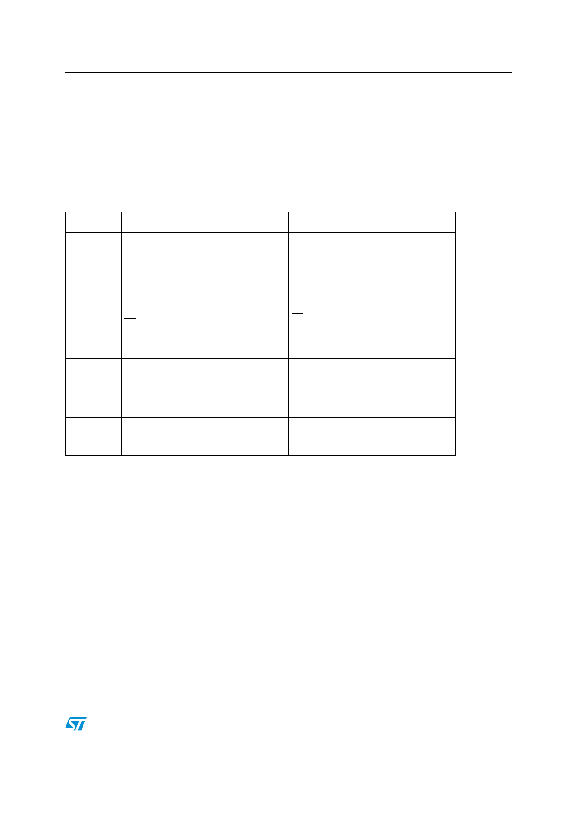
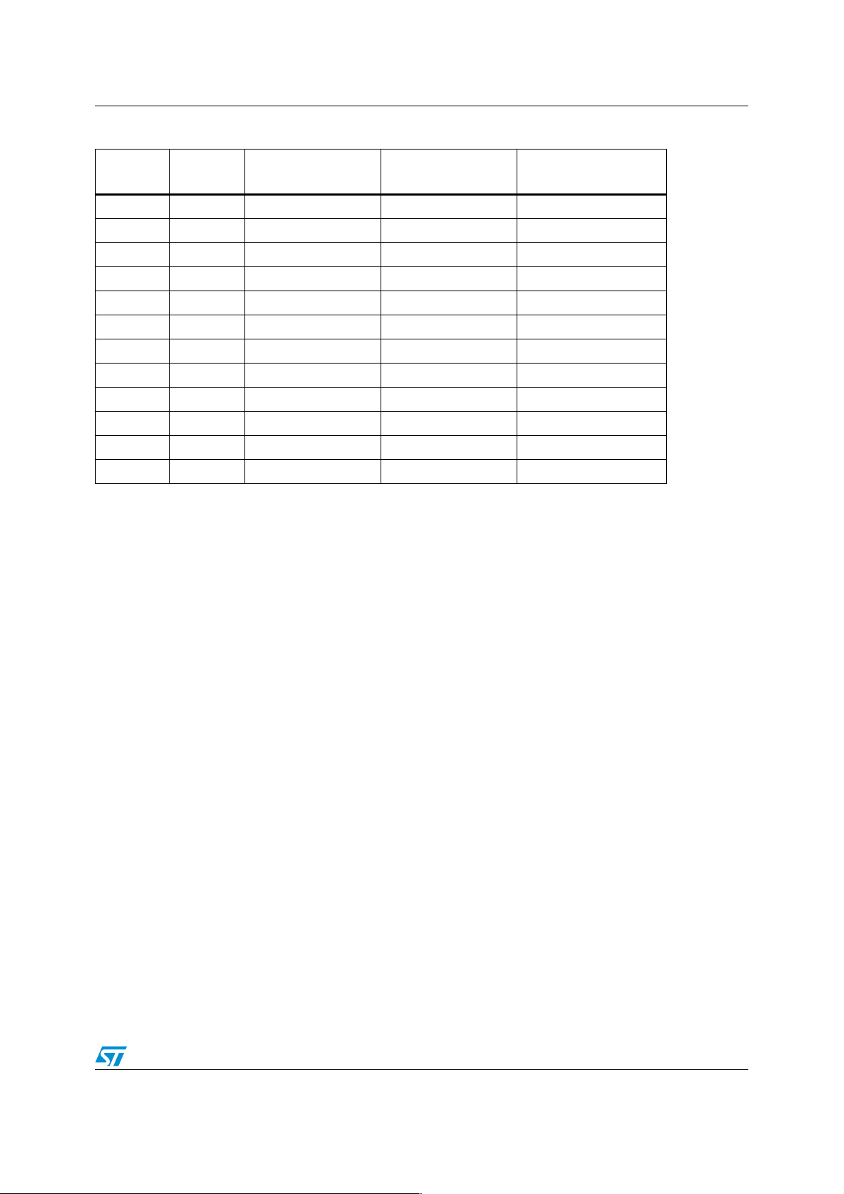
Ta bl e 1 summarizes the modifications made in the pinout.
Table 1. Pinout modifications
Pin number ST10F269Zx name and function ST10F276Z5 name and function
DC: Internal voltage regulator decoupling.
17
56
99
143 VSS: Ground pin
Connect to nearest V
capacitor.
DC1: Internal voltage regulator
decoupling. Connect to nearest V
330nF capacitor.
EA: Selects code execution out of internal
Flash memory or external memory
according to level during reset.
via a 330 nF
SS
SS
via a
: 5 V power supply pin
V
DD
V18: Internal voltage regulator
decoupling. Connect to nearest VSS via a
10-100nF capacitor.
-V
EA
internal Flash memory or external
memory according to level during reset.
Power supply input for standby mode.
XTAL3: Input to the 32 kHz oscillator
amplifier circuit. When not used shall be
tied to ground to avoid consumption.
Besides, bit OFF32 in RTCCON register
must be set.
: Selects code execution out of
STBY
XTAL4: Output of the 32 kHz oscillator
144 V
: 5V power supply pin
DD
amplifier circuit. When not used must be
left open to avoid spurious consumption.
1.1.2 Pin 17
On the ST10F269Zx, a decoupling capacitor of 330nF minimum has to be connected between the pin 17
(named DC2) and the nearest V
This is no longer the case for the ST10F276Z5 device where pin 17 is a V
Hardware impact
PCB must be adapted.
Software impact
None.
SS
pin.
DD
pin.
3/33

AN2555 - Application note Modified features
1.1.3 Pin 56
On the ST10F269Zx, a decoupling capacitor of 330nF minimum has to be connected between the pin 56
(named DC1) and the nearest V
On the ST10F276Z5, pin 56 is named V
maximum must be connected between it and the nearest V
SS
pin.
and a capacitor of value between 10nF minimum to 100nF
18
SS
pin.
Hardware impact
Change on the capacitor value. As the value is much lower, the footprint of the capacitor might be smaller
and a modification of the PCB might be needed.
Software impact
None.
1.1.4 Pin 99
On the ST10F269Zx, pin 99 is EA and used upon reset to select the start from the internal Flash memory
or the external memory.
On the ST10F276Z5, pin 99 has the additional function of providing the 5V power supply to the device in
standby mode (new power-saving mode), it is called EA
-V
STBY
.
Hardware impact
The modification depends on the previous use of the ST10F269Zx and on whether the Standby mode is
used or not.
For an application where the Standby mode is not used, no change to the PCB is required. If the new
application uses the Standby mode, the EA
-V
pin must be separated from the common 5V and have
STBY
a specific supply path.
Software impact
None.
1.1.5 Pins 143 and 144
These pins are VSS and VDD, respectively, in the ST10F269Zx. On the ST10F276Z5 they are used as
XTAL3 and XTAL4 for connection to an optional 32 kHz crystal to clock the Real Time Clock during
power-down.
Hardware impact
PCB must be redesigned.
If the optional 32 kHz is not used:
● pin 143 (XTAL3) must be linked to ground like on the ST10F269Zx
● pin 144 (XTAL4) must be left open. It can also be connected to ground via a capacitor to reduce the
potential RF noise that might be propagated inside the device if the pin is left floating.
4/33

AN2555 - Application note Modified features
Software impact
In case the optional 32 kHz is not used, the OFF32 bit of the RTCCON register must be set. Prior to
setting the OFF32 bit in RTCCON register, the RTC must be enabled by setting RTCEN, bit 4 of
XPERCON, and XPEN, bit 3 of SYSCON.
1.2 XRAM
The ST10F269Zx has 10 Kbytes of extension RAM whereas the ST10F276Z5 has 66 Kbytes.
The XRAM of the ST10F269Zx is divided into 2 ranges, XRAM1 of 2 Kbytes and XRAM2 of 8 Kbytes:
● The XRAM1 address range is 00’E000h - 00’E7FFh if enabled (XPEN and XRAM1EN, bit 2 of
SYSCON register and of XPERCON register, respectively, must both be set).
● The XRAM2 address range is 00’C000h - 00’DFFFh if enabled (XPEN and XRAM2EN, bit 2 of
SYSCON register and bit 3 of XPERCON register, respectively, must both be set).
The XRAM of the ST10F276Z5 is divided into 2 ranges, XRAM1 of 2 Kbytes and XRAM2 of 64 Kbytes:
● The XRAM1 address range is 00’E000h - 00’E7FFh if enabled (XPEN and XRAM1EN, bit 2 of
SYSCON register and bit 2 of XPERCON register, respectively, must both be set).
● The XRAM2 address range is 0F’0000h - 0F’FFFFh if enabled (XPEN and XRAM2EN, bit 2 of
SYSCON register and bit 3 of XPERCON register, respectively, must both be set).
1.2.1 Hardware impacts
None.
1.2.2 Software impacts
There is no change in the enabling of the XRAM blocks: XPERCON register bits, XRAM1EN and
XRAM2EN, and SYSCON register bit, XPEN, are used to enable them.
The memory mapping of the application is impacted by the different XRAM size and the different location
of XRAM2 in segment 15. In the ST10F269Zx the whole XRAM is in page 3 of segment 0.
Variables and PEC transfers
For architecture reasons, the PEC destination and source pointers must be in segment 0. Therefore all
RAM variables and arrays that will be PEC addressed must be located within either the DPRAM
(00’F600h - 00’FDFFh) or XRAM1 (00’E000h - 00’E7FFh).
About Toolchain memory model
A change in the Toolchain configuration is needed to take into account the new XRAM2 location. In the
ST10F269Zx, the entire XRAM is in page 3 and is then automatically addressed using DPP3 that points
to page 3 (in order to access the DPRAM and the SFR/ESFR). For the ST10F276Z5, it is necessary to
dedicate a DPP to access some of XRAM2.
Example in case of Small Memory Model with Tasking toolchain
The Small memory model makes it possible to have a total code size up to 16 Mbytes, up to 64 Kbytes of
fast accessible 'normal user data' in three different memory configurations and the possibility to access
far/huge data, if more than 64 Kbytes of data is needed.
5/33
AN2555 - Application note Modified features
The three memory configurations possible for this 64 Kbytes of 'normal user data' are:
● Default
The four DPP registers are assumed to contain their system startup value (0-3), providing one linear
data area of 64 Kbytes in the first segment (00’0000h - 00’FFFFh).
● Addresses Linear
DPP3 contains page number 3, allowing access to ST10 registers and bit-addressable memory.
DPP0 - DPP2 provide a linear data area of 48 Kbytes anywhere in memory.
● Paged
DPP3 contains page number 3, allowing access to ST10 registers and bit-addressable memory.
DPP0, DPP1 and DPP2 contain the page numbers of data areas of 16 Kbytes anywhere in memory.
The Default configuration can no longer be used. The other configurations offer the following possibilities:
● with the Addresses Linear configuration the XRAM2 block is almost entirely covered with DPPs but
then accesses to constants must be made via EXTP instructions.
● In the Paged configuration up to two DPPs can be assigned to XRAM2 and one DPP for constants.
1.3 Flash EEPROM
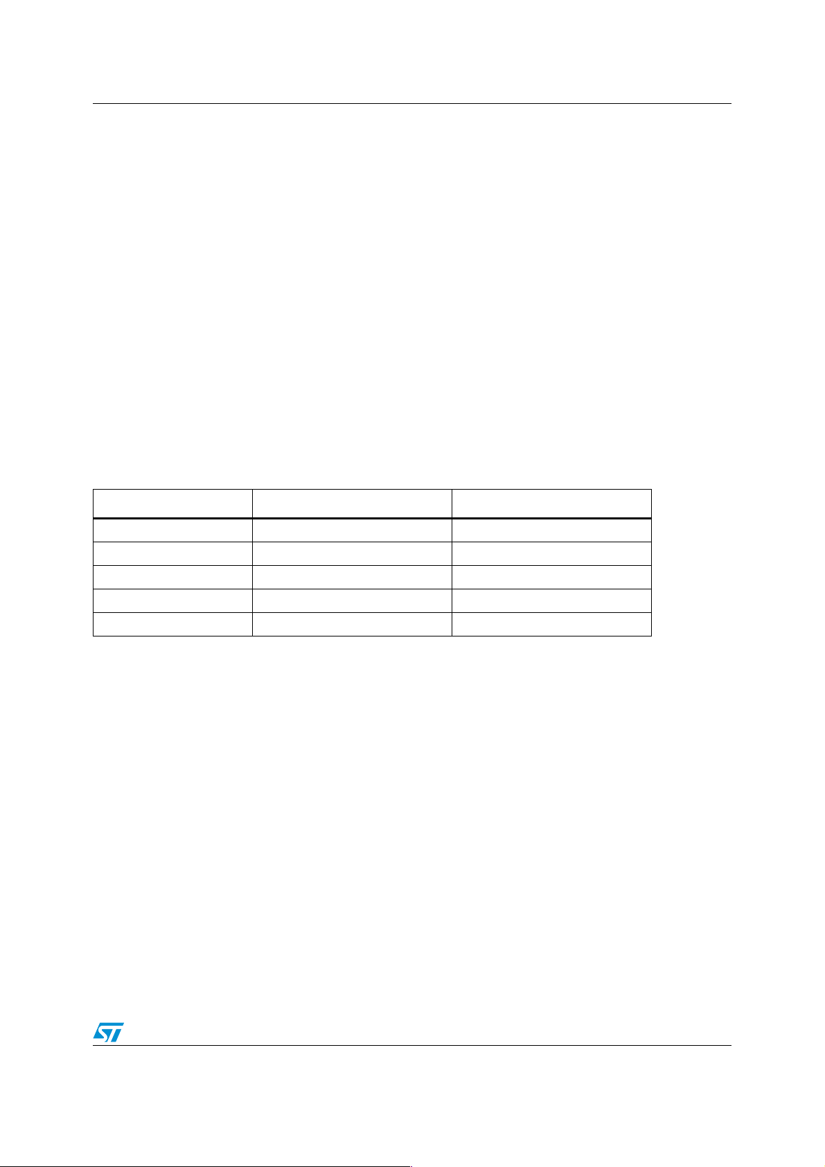
Table 2. Flash memory key characteristics
ST10F269Zx ST10F276Z5
Flash Size 256 Kbytes 832 KBytes
Flash Organization 7 blocks 4 banks, 17 blocks
Programming voltage 5 Volts 5 Volts
Programming method Write/Erase Controller Write/Erase Controller
Program/Erase cycles 100000 cycles 100000 cycles
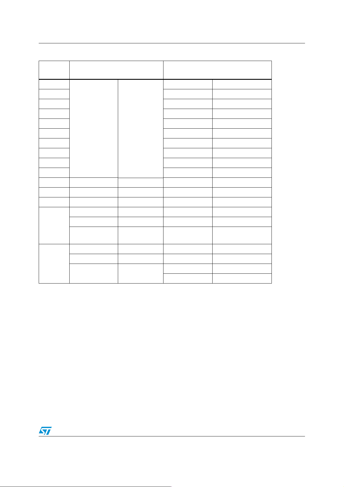
Table 3: Flash memory mapping shows the Flash memory address ranges of the 2 devices.
6/33
AN2555 - Application note Modified features
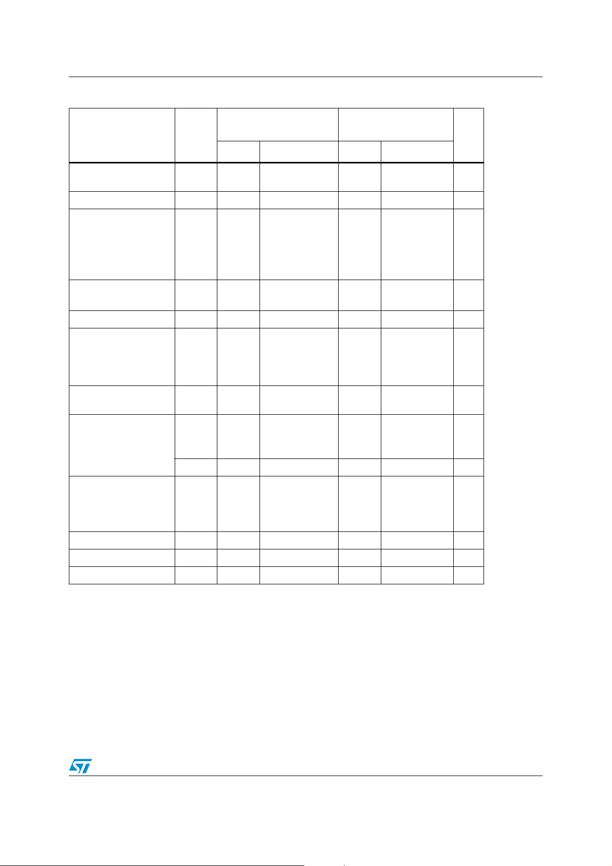
Table 3. Flash memory mapping
Segment
number
14
13 0D’0000 - 0D’FFFF X-Bank3, Block1: 64KB
12 0C’0000 - 0C’FFFF X-Bank3, Block0: 64KB
11 0B’0000 - 0B’FFFF X-Bank2, Block2: 64KB
10 External memory 0A’0000 - 0A’FFFF X-Bank2, Block1: 64KB
9 09’0000 - 09’FFFF X-Bank2, Block0: 64KB
8 08’0000 - 08’FFFF I-Bank1, Block1: 64KB
7 07’0000 - 07’FFFF I-Bank1, Block0: 64KB
6 06’0000 - 06’FFFF I-Bank0, Block9: 64KB
5 05’0000 - 05’FFFF I-Bank0, Block8: 64KB
4 04’0000 - 04’FFFF Block6: 64KB 04’0000 - 04’FFFF I-Bank0, Block7: 64KB
3 03’0000 - 03’FFFF Block 5: 64KB 03’0000 - 03’FFFF I-Bank0, Block6: 64KB
2 02’0000 - 02’FFFF Block 4: 64KB 02’0000 - 02’FFFF I-Bank0, Block5: 64KB
1
ST10F269Zx Flash mapping ST10F276Z5 Flash mapping
0E’0000 - 0E’FFFF Flash registers
05’0000 - 0E’FFFF
01’8000 - 01’FFFF Block 3: 32KB 01’8000 - 01’FFFF I-Bank0, Block4: 32KB
01’0000 - 01’7FFF External memory 01’0000 - 01’7FFF External memory
00’8000 - 00’FFFF
00’6000 - 00’7FFF Block 2: 8KB 00’6000 - 00’7FFF I-Bank0, Block3: 8KB
External memory
Internal RAM
00’8000 - 00’FFFF
External memory
Internal RAM
0
00’4000 - 00’5FFF Block 1: 8KB 00’4000 - 00’5FFF I-Bank0, Block2: 8KB
00’2000 - 00’3FFF I-Bank0, Block1:8KB
00’0000 - 00’3FFF Block 0: 16KB
00’0000 - 00’1FFF I-Bank0, Block0: 8KB
1.3.1 Hardware impacts
None.
1.3.2 Software impacts
The mapping of the application, the programming and erasing routines are impacted.
1.4 A/D converter
In the ST10F276Z5, the Analog Digital converter has been re-designed (compared to the A/D converter
in the ST10F269Zx). The ST10F276Z5 still provides an Analog / Digital Converter with 10-bit resolution
and an on-chip sample & hold circuit.
1.4.1 Hardware / Software impact: conversion timing control
The A/D Converter in the ST10F276Z5 is not fully compatible to that in the ST10F269Zx (timing and
programming model).
7/33
AN2555 - Application note Modified features
In the ST10F269Zx, the sample time (to charge the capacitors) and the conversion time are
programmable and can be adjusted to the external circuitry. The total conversion time is compatible with
the formula used for ST10F269Zx, while the meanings of the ADCTC and ADSTC bit fields are no longer
compatible.
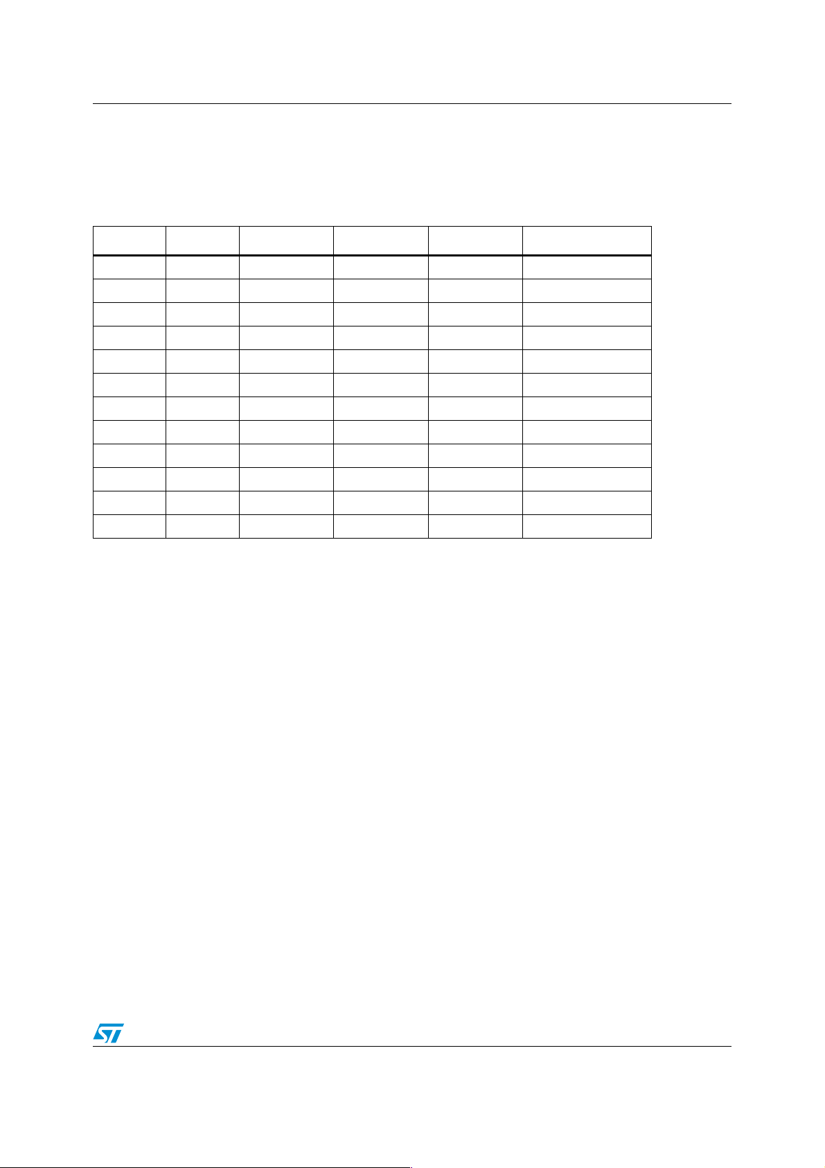
Table 4. ST10F276Z5 conversion timing table
ADCTC ADSTC Sample Comparison Extra Total Conversion
00 00 TCL * 120 TCL * 240 TCL * 28 TCL * 388
00 01 TCL * 140 TCL * 280 TCL * 16 TCL * 436
00 10 TCL * 200 TCL * 280 TCL * 52 TCL * 532
00 11 TCL * 400 TCL * 280 TCL * 44 TCL * 724
11 00 TCL * 240 TCL * 120 TCL * 52 TCL * 772
11 01 TCL * 280 TCL * 560 TCL * 28 TCL * 868
11 10 TCL * 400 TCL * 560 TCL * 100 TCL * 1060
11 11 TCL * 800 TCL * 560 TCL * 52 TCL * 1444
10 00 TCL * 480 TCL * 960 TCL * 100 TCL * 1540
10 01 TCL * 560 TCL * 1120 TCL * 52 TCL * 1732
10 10 TCL * 800 TCL * 1120 TCL * 196 TCL * 2116
10 11 TCL * 1600 TCL * 1120 TCL * 164 TCL * 2884
The parameter to take care of is the Sample time: This is the time during which the capacitances of the
converter are charged via the respective analog input pins. Table 5: ST10F276Z5 vs. ST10F269Zx
sample time comparison table shows the respective sample times of the 2 devices.
8/33
AN2555 - Application note Modified features
Table 5. ST10F276Z5 vs. ST10F269Zx sample time comparison table
ADCTC ADSTC
00 00 TCL * 48 TCL * 120 2.5
00 01 TCL * 96 TCL * 140 1.46
00 10 TCL * 192 TCL * 200 1.04
00 11 TCL * 384 TCL * 400 1.04
11 00 TCL * 96 TCL * 240 2.5
11 01 TCL * 192 TCL * 280 1.46
11 10 TCL * 384 TCL * 400 1.04
11 11 TCL * 768 TCL * 800 1.04
10 00 TCL * 192 TCL * 480 2.08
10 01 TCL * 384 TCL * 560 1.46
10 10 TCL * 768 TCL * 800 1.04
10 11 TCL * 1538 TCL * 1600 1.04
ST10F269Zx Sample
Time
ST10F276Z5 Sample
Time
Ratio F276Z5 / F269Zx
In the default configuration the sample time of the ST10F276Z5 is 2.5 times longer compared to that of
the ST10F269Zx. This has an impact on the frequency of the input signal that can be applied to the
ST10F276Z5.
1.4.2 Hardware impacts
Electrical characteristics
Ta bl e 6 lists the differences in the DC characteristics of the two devices. The main points are:
● I
● C
● DNL, INL and OFS are different: the ADC conversion curves for the 2 devices are different.
is 10 times higher on the ST10F276Z5. The V
AREF
pad must therefore be directly connected
AREF
to the power supply: Connecting a resistor would create a voltage shift in the analog reference.
, input pin capacitances are different.
AIN
9/33
AN2555 - Application note Modified features
Table 6. ADC differences
Parameter Symbol
Analog Reference
voltage
V
Analog Input Voltage V
ADC Input capacitance
Port5, Not sampling
Port5, Sampling
Port1, Not Sampling
Port1, sampling
Sample time t
Conversion time t
Total Unadjusted Error
Por t5
Port1 - No overload
Port1 - Overload
Internal resistance of
analog source
R
AREF
AIN
C
AIN
S
C
TUE
ASRC
Limit values for
ST10F269Zx
Limit values for
ST10F276Z5
min. max. min. max.
4.0 VDD + 0.1 4.5 V
V
AGND
V
AREF
V
AGND
C
-
-
-
-
48TCL 1536TCL
10
15
N.A.
N.A.
-
-
-
-
1µs
120TCL
V
AREF
+ CP2 +C
P1
10.5
12.5
1600TCL
DD
7
9
388TCL 2884TCL 388TCL 2884TCL
-2.0
-
-
+2.0
-
-
-2.0
-5.0
-7.0
+2.0
+5.0
+7.0
tS[ns]/150 - 0.25 kΩ
Unit
V
V
S
pF
LSB
R
SW
Analog switch
resistance
Por t5
Por t1
R
AD
N.A. N.A. -
-
600
1000
N.A. N.A. - 1300 Ω
Ω
Reference supply
current
running mode
power-down mode
I
AREF
-
-
500
1
-
-
5000
1
µA
Differential Nonlinearity DNL -0.5 +0.5 1 1 LSB
Integral Nonlinearity INL -1.5 +1.5 -1.5 1.5 LSB
Offset Error OFS -1.0 +1.0 -1.5 1.5 LSB
Note: The V
pin is also used as a supply pin for the ADC module. As there is a higher current
AREF
sink on this pin on the ST10F276Z5 compared to the ST10F269Zx, it is recommended not
to connect a resistor (for example because of an RC filter), to prevent creating an offset in
the reference.
1.4.3 Software impacts
Self-calibration and ADC initialization routine
An automatic self-calibration adjusts the ADC module to process parameter variations at each reset
event. After reset, the busy flag (read-only) ADBSY is set because the self-calibration is ongoing. The
10/33
 Loading...