

AN2544
Application note
Designing a low cost power supply using a
VIPer12/22A-E in a buck configuration
Introduction
Many appliances today use nonisolated power supply to furnish low output power required
to run a micro, LED display, and a few relays or AC switches. This type of power supply has
a single rectifier so as to reference the neutral to output ground in order to fire TRIACs or AC
switches. This article describes the use of the VIPer12A-E and the VIPer22A-E which are
pin-for-pin compatible and can supply power for many applications. This paper provides an
off-line, nonisolated power supply evaluation board based on the VIPer12/22A-E. Four
different examples are covered. The VIPer12A-E is used for 12 V at 200 mA and 16 V at 200
mA. The VIPer22A-E is used for 12 V at 350 mA and 16 V at 350 mA. The same board can
be used for any output voltage from 10 V to 35 V. For outputs less than 16 V, D6 and C4 are
populated and W1 is omitted. For outputs greater than 16 V, D6 and C4 are omitted and W1
is populated. For more design detail, see AN1357 "VIPower: low cost power sullies using
the VIPer12A-E in nonisolated application." The objective of this application note is to
familiarize the end user with this reference design and to quickly modify it for different
voltage output. This design gives:
■ Lowest possible component count
■ Integrated thermal overload protection
■ About 200 mW at no-load consumption
■ Efficiency measured between 70% to 80% at full load
■ Integrated Short circuit protection
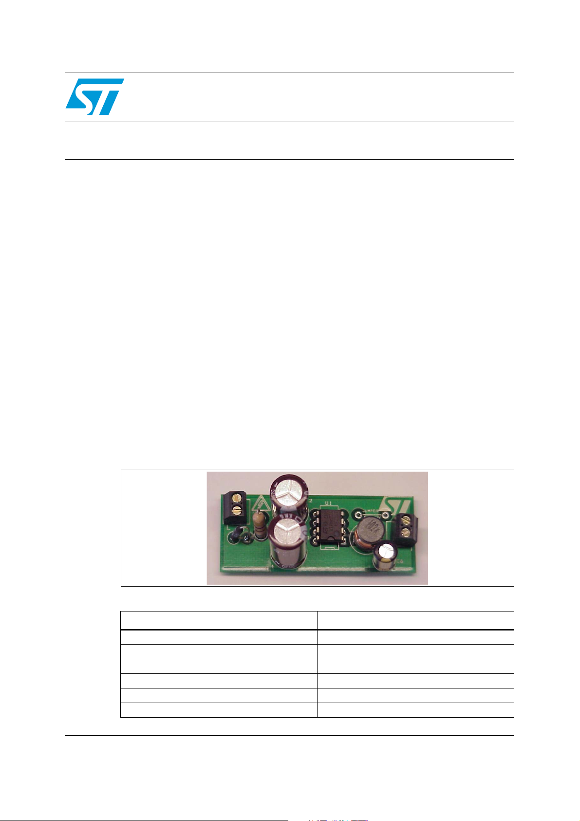
Figure 1. Evaluation board (STEVAL-ISA035V1)
Table 1. Operating conditions for the four samples
Board version (with changes) Output voltage and current
Input voltage range 85 V
Input voltage frequency range 50/60 Hz
Output version 1 VIPer22ADIP-E 12 V at 350 mA 4.2 W
Output version 2 VIPer12ADIP-E 12 V at 200 mA 2.4 W
Output version 3 VIPer22ADIP-E 16 V at 350 mA 5.6 W
Output version 4 VIPer12ADIP-E 16 V at 200 mA 3.2 W
November 2007 Rev 4 1/17
to 264 V
ac
ac
www.st.com

Contents AN2544
Contents
1 Circuit operation . . . . . . . . . . . . . . . . . . . . . . . . . . . . . . . . . . . . . . . . . . . . 4
1.1 Input line rectification and line conducted filter . . . . . . . . . . . . . . . . . . . . . . 4
1.2 Start circuit . . . . . . . . . . . . . . . . . . . . . . . . . . . . . . . . . . . . . . . . . . . . . . . . . 4
1.3 Inductor selection . . . . . . . . . . . . . . . . . . . . . . . . . . . . . . . . . . . . . . . . . . . . 5
1.4 Design example . . . . . . . . . . . . . . . . . . . . . . . . . . . . . . . . . . . . . . . . . . . . . 5
1.5 Design hints and trade-off . . . . . . . . . . . . . . . . . . . . . . . . . . . . . . . . . . . . . 5
1.6 Board layout . . . . . . . . . . . . . . . . . . . . . . . . . . . . . . . . . . . . . . . . . . . . . . . . 9
1.7 Burst mode in no-load or very light load . . . . . . . . . . . . . . . . . . . . . . . . . . 11
1.8 Short circuit . . . . . . . . . . . . . . . . . . . . . . . . . . . . . . . . . . . . . . . . . . . . . . . 12
1.9 Performance . . . . . . . . . . . . . . . . . . . . . . . . . . . . . . . . . . . . . . . . . . . . . . . 13
1.10 EMI conducted . . . . . . . . . . . . . . . . . . . . . . . . . . . . . . . . . . . . . . . . . . . . . 15
2 Conclusion . . . . . . . . . . . . . . . . . . . . . . . . . . . . . . . . . . . . . . . . . . . . . . . . 16
3 Revision history . . . . . . . . . . . . . . . . . . . . . . . . . . . . . . . . . . . . . . . . . . . 16
2/17

AN2544 List of figures
List of figures
Figure 1. Evaluation board (STEVAL-ISA035V1) . . . . . . . . . . . . . . . . . . . . . . . . . . . . . . . . . . . . . . . . 1
Figure 2. Inductor current: 470 µH VS 1000 µH. . . . . . . . . . . . . . . . . . . . . . . . . . . . . . . . . . . . . . . . . . 6
Figure 3. Schematic for 12 V at 350 mA . . . . . . . . . . . . . . . . . . . . . . . . . . . . . . . . . . . . . . . . . . . . . . . 7
Figure 4. Schematic for 16 V at 350 mA . . . . . . . . . . . . . . . . . . . . . . . . . . . . . . . . . . . . . . . . . . . . . . . 8
Figure 5. Composite. . . . . . . . . . . . . . . . . . . . . . . . . . . . . . . . . . . . . . . . . . . . . . . . . . . . . . . . . . . . . . . 9
Figure 6. Top side . . . . . . . . . . . . . . . . . . . . . . . . . . . . . . . . . . . . . . . . . . . . . . . . . . . . . . . . . . . . . . . . 9
Figure 7. Bottom side and surface mount components (viewed from top) . . . . . . . . . . . . . . . . . . . . . . 9
Figure 8. Bad start . . . . . . . . . . . . . . . . . . . . . . . . . . . . . . . . . . . . . . . . . . . . . . . . . . . . . . . . . . . . . . . 11
Figure 9. Good start . . . . . . . . . . . . . . . . . . . . . . . . . . . . . . . . . . . . . . . . . . . . . . . . . . . . . . . . . . . . . . 11
Figure 10. Burst mode . . . . . . . . . . . . . . . . . . . . . . . . . . . . . . . . . . . . . . . . . . . . . . . . . . . . . . . . . . . . . 12
Figure 11. Operation during a short . . . . . . . . . . . . . . . . . . . . . . . . . . . . . . . . . . . . . . . . . . . . . . . . . . . 12
Figure 12. Load regulations for 12 V output. . . . . . . . . . . . . . . . . . . . . . . . . . . . . . . . . . . . . . . . . . . . . 14
Figure 13. Line regulation . . . . . . . . . . . . . . . . . . . . . . . . . . . . . . . . . . . . . . . . . . . . . . . . . . . . . . . . . . 14
Figure 14. Efficiency . . . . . . . . . . . . . . . . . . . . . . . . . . . . . . . . . . . . . . . . . . . . . . . . . . . . . . . . . . . . . . 15
Figure 15. VIPer22-E, 12 V at 350 mA output . . . . . . . . . . . . . . . . . . . . . . . . . . . . . . . . . . . . . . . . . . . 15
Figure 16. VIPer12-E, 12 V at 200 mA output . . . . . . . . . . . . . . . . . . . . . . . . . . . . . . . . . . . . . . . . . . . 15
Figure 17. VIPer22-E, 16 V at 350 mA output . . . . . . . . . . . . . . . . . . . . . . . . . . . . . . . . . . . . . . . . . . . 16
Figure 18. VIPer12-E, 16 V at 200 mA output . . . . . . . . . . . . . . . . . . . . . . . . . . . . . . . . . . . . . . . . . . . 16
3/17

Circuit operation AN2544
1 Circuit operation
1.1 Input line rectification and line conducted filter
The circuit operations for all four versions are basically the same. The difference is in the
circuit for startup. Version 1 will be described here with reference to Figure 3. The output of
the converter is not isolated from the input. This makes neutral common to output ground
thus giving a reference back to neutral. The buck is less expensive due to the fact that it
does not use a transformer and an opto coupler. The AC line is applied through D1 which
rectifies the line input every other half cycle.
C1, L0, C2 form a pie filter to reduce EMI noise. The value of the capacitor is chosen to
maintain a reasonable valley, because the caps are charged every other half cycle. Two
diodes can be used in place of D1 to sustain burst pulses of 2 kV. R10 serves two purposes,
one is for inrush limiting and the other is to act as a fuse in case of a catastrophic failure. A
wire wound resistor handles the energy of the inrush. Flame proof resistor and a fuse can be
used depending on system and safety requirements. C7 helps the EMI by balancing line and
neutral noise without using an Xcap. This will pass EN55022 level "B". If the requirement is
less, then this cap can be left out of the circuit.
1.2 Start circuit
The voltage across C2 is fed to the drain, pin 5 through 8. Inside the VIPer, the constant
current source delivers 1mA to the V
the V
pulsing. During this time, the energy is being supplied from the V
must be greater than the energy needed to supply the output current plus the energy to
charge of the output capacitor, before the V
Figure 8 and Figure 9. The value of the capacitor is therefore chosen to accommodate the
startup time. During a short circuit, the V
the internal high voltage current generator to initiate a new startup sequence. The charging
and discharging of the capacitor determine the time period that the power supply is to be on
and off. This reduces the RMS heating effect on all components. The regulation circuit
consists of Dz, C4 and D8. D8 peak charges C4 during the freewheeling time when D5 is
conducting. During this time, the source or reference to the VIPer is one diode drop below
ground, which compensates for the D8 drop. So basically the Zener voltage is the same as
the output voltage. C4 is connected across V
is a BZT52C12, ½ W Zener with a specified test current of 5 mA. These Zeners that are
specified at a lower current give better accuracy of the output voltage. If the output voltage is
lower than 16 V, the circuit can be configured as in Figure 3 where V
V
case condition. A 16 V Zener with a 5% low tolerance can be 15.2 V plus the internal
resistance to ground is 1230 Ω which is an additional 1.23 V for a total of 16.4 V. For 16 V
output and higher, the V
similar to Figure 4.
pin reaches 14.5 V nominal, the current source turns off and the VIPer starts
dd
pin. When the internal current source charges the Vdd cap, Vdd can reach 16V at worse
fb
pin 4. This current charges C3. When the voltage on
dd
cap. The energy stored
dd
cap falls below 9 V. This can be seen in
dd
cap discharges below the minim value enabling
dd
and source to filter the regulation voltage. Dz
fb
is separated from the
dd
pin and the Vfb pin can share a common diode and capacitor filter
dd
4/17

AN2544 Circuit operation
1.3 Inductor selection
A starting point for the inductor operating in discontinuous mode can be derived from the
following formula which gives a good approximation of the inductor.
Equation 1
Pout
------------------------------- -
•=
L2
()2f•
Id
peak
Where Id
is the minimum peak drain current, 320 mA for the VIPer12A-E and 560 mA for
peak
the VIPer22A-E, f is the switching frequency at 60 kHz. The maximum peak current limits
the power delivered in the buck topology. Therefore, the calculation above is for an inductor
that operates in discontinuous mode. If the current swings down to zero, than the peak
current is twice the output. This limits the output current to 280 mA for a VIPer22A-E. If the
inductor is a larger value, operating between continuous and discontinuous mode, we can
reach 200 mA comfortably away from the current limit point. C6 has to be a low ESR
capacitor to give the low ripple voltage
Equation 2
D5 needs to be a fast recovery diode but D6 and D8 can be standard diodes. DZ1 is used to
clamp the voltage to 16 V. The nature of the buck topology is to peak charge at no-load. A
Zener 3 to 4 V higher than the output voltage is recommended.
1.4 Design example
Figure 3 is the schematic for the evaluation board. It is set up for 12 V with a maximum
current of 350 mA. If less current is required, then the VIPer22A-E can be changed to a
VIPer12A-E and C2 can be decreased from 10 µf to 4.7 µF. This delivers up to 200 mA.
Figure 4 shows the same board but for 16 V output or higher, D6 and C4 can be left out. The
jumper bridges the output voltage to the V
V
rippleIripple
pin.
dd
Cesr•=
1.5 Design hints and trade-off
The value of L determines the boundary condition between continuous and discontinuous
mode for a given output current. In order to operate in discontinuous mode, the inductor
value has to be lower than
Equation 3
L
Where R is the load resistance, T is the switching period, and D is the duty cycle.
There are two points to consider. One is, the more discontinuous the higher the peak
current. This point should be kept lower than the minimum pulse by pulse current limit of the
VIPer22A-E which is 0.56 A. The other is if we use a larger value inductor to run continuous
all of the time, we run into excess heat from switching losses of the MOSFET inside the
VIPer. Of course, the inductor current rating must be higher than the output current to
prevent the risk of saturating the core.
1
-- -
RT 1D–()•••=
2
5/17

Circuit operation AN2544
Figure 2. Inductor current: 470 µH VS 1000 µH
The blue trace is the current with 470 µH inductor and the purple trace is the current with a
1000 µH inductor.
On the above scope plot in Figure 2, the trace represents the current going through the
inductor. Current charges up the inductor during the time the MOSFET is on. At this time,
the source pin is the same as the rectified line input and the current is ramping up. At 350
mA output current, the peak of the current is 550 mA for a 470 µH inductor, the blue trace.
The worse case condition for the VIPer Idlim is 560 mA. So therefore we are close to the
pulse by pulse current limit trip point. This is manifested by the output voltage dropping as
the output current is being raised past the limit. 470 µH inductor is the minimum value that
can be used from the calculations for a 350 mA output. A good compromise is a 1000 µH
making the swing less, keeping the peak at 443 mA, away from the 560 mA current limit.
Looking at the purple trace the turn-on losses are increased and the turn-off losses are
decreased in the MOSFET inside the VIPer.
It is best to choose the inductor to give ½ the ripple current between discontinuous to
continuous. This is the best compromise when working close to the maximum current. The
trade-off is a little more heat for the safety margin away from the current trip point.
VIPer temperature rise with two different inductors at 350 mA is:
Table 2. VIPer temperature rise with different inductors
Inductor Maximum peak current VIPer22ADIP-E temperature rise
470 µH 550 mA 34 °C
1000 µH 443 mA 40.5 °C
6/17
 Loading...