

Page 1
AN2531
Application note
Generating multicolor light using RGB LEDs
Introduction
The new high power and brightness RGB LEDs are coming to be used in many different
lighting applications as backlighting, general lighting systems, traffic signals, automotive
lighting, advertising signs, etc. They are becoming popular mainly because it is possible to
generate an easy multicolor light with special lighting effects and their brightness can be
easy changed. On top of this, their long lif etime and small siz e make them the light source of
the future.
This document describes how to drive RGB LEDs, how to calculate a power dissipation,
how to design an over temperature protection, how to use a software PWM modulation and
why over voltage protection should be implemen ted for this kind of application.
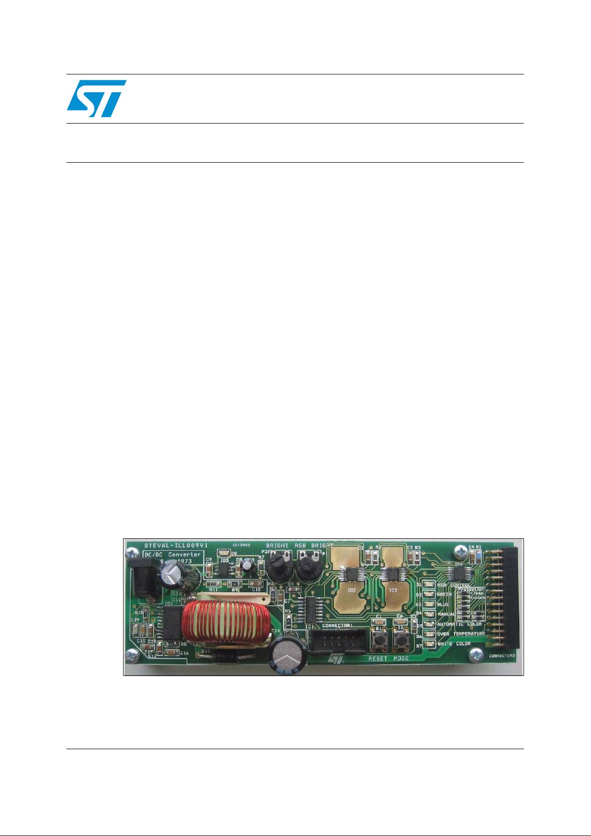
STEVAL-ILL009V1 reference board shown in Figure 1 was developed in order to
demonstrate this design concept. This board was designed f o r driving super high brightness
multicolor RGB LEDs with current up to 700 mA per L ED. The LED brightness and color can
be very easy changed by potentiometers a nd an automatic color change mode continuously
modulates the color of the LED to generate multicolor light. The LED over-temperature
protection is designed on this board and therefore the power delivered to the LED can be
automatically limited to prevent LED overheating.
The STEVAL-ILL009V1 is a mother board assembled without LEDs. To evalua te light effect
features, it is ne cessary to order a load board (additional board wit h assembled RGB LEDs).
Two load boards are available for easy performance evaluation. The first one with the
OSTAR Projection Module (refer to Chapter 11, point 1) has ordering code STEVALILL009V3 and the second one with the Golden Dragon LEDs (refer to Chapter 11, point 2)
has ordering code STEVAL-ILL009V4. All technical information about these reference
boards such as bill of materials, schematics, software, temperature protection and so on are
described in the sections below.
Figure 1. STEVAL-ILL009V1 reference board
May 2007 Rev 1 1/37
www.st.com
Page 2

Contents AN2531
Contents
1 Driving concept for RGB LEDs . . . . . . . . . . . . . . . . . . . . . . . . . . . . . . . . 6
2 How to drive many LEDs . . . . . . . . . . . . . . . . . . . . . . . . . . . . . . . . . . . . . 7
3 How to set high current for LEDs . . . . . . . . . . . . . . . . . . . . . . . . . . . . . . 9
4 Color control - software modulation . . . . . . . . . . . . . . . . . . . . . . . . . . . 10
5 Power dissipation . . . . . . . . . . . . . . . . . . . . . . . . . . . . . . . . . . . . . . . . . . 12
6 Over-voltage protection . . . . . . . . . . . . . . . . . . . . . . . . . . . . . . . . . . . . . 14
6.1 Description . . . . . . . . . . . . . . . . . . . . . . . . . . . . . . . . . . . . . . . . . . . . . . . . 14
6.2 Type of solutions . . . . . . . . . . . . . . . . . . . . . . . . . . . . . . . . . . . . . . . . . . . . 15
7 LED temperature protection . . . . . . . . . . . . . . . . . . . . . . . . . . . . . . . . . . 16
8 STEVAL-ILL009V1 reference board . . . . . . . . . . . . . . . . . . . . . . . . . . . . 17
8.1 General description . . . . . . . . . . . . . . . . . . . . . . . . . . . . . . . . . . . . . . . . . 17
8.2 Getting started . . . . . . . . . . . . . . . . . . . . . . . . . . . . . . . . . . . . . . . . . . . . . 18
8.3 Schematic description . . . . . . . . . . . . . . . . . . . . . . . . . . . . . . . . . . . . . . . 19
8.4 Bill of materials (BOM) . . . . . . . . . . . . . . . . . . . . . . . . . . . . . . . . . . . . . . . 22
8.5 Design calculation . . . . . . . . . . . . . . . . . . . . . . . . . . . . . . . . . . . . . . . . . . 23
8.5.1 LED supply voltage . . . . . . . . . . . . . . . . . . . . . . . . . . . . . . . . . . . . . . . . 23
8.5.2 Temperature protection . . . . . . . . . . . . . . . . . . . . . . . . . . . . . . . . . . . . . 23
8.5.3 SW PWM frequency calculation . . . . . . . . . . . . . . . . . . . . . . . . . . . . . . 25
8.6 Software . . . . . . . . . . . . . . . . . . . . . . . . . . . . . . . . . . . . . . . . . . . . . . . . . . 26
9 STEVAL-ILL009V3 Load board . . . . . . . . . . . . . . . . . . . . . . . . . . . . . . . . 30
9.1 Schematic description . . . . . . . . . . . . . . . . . . . . . . . . . . . . . . . . . . . . . . . 30
9.2 Bill of materials . . . . . . . . . . . . . . . . . . . . . . . . . . . . . . . . . . . . . . . . . . . . . 31
10 STEVAL-ILL009V4 Load board . . . . . . . . . . . . . . . . . . . . . . . . . . . . . . . . 33
10.1 Schematic description . . . . . . . . . . . . . . . . . . . . . . . . . . . . . . . . . . . . . . . 34
10.2 Bill of materials . . . . . . . . . . . . . . . . . . . . . . . . . . . . . . . . . . . . . . . . . . . . . 34
2/37
Page 3

AN2531 Contents
11 Reference and related materials . . . . . . . . . . . . . . . . . . . . . . . . . . . . . . 36
12 Revision history . . . . . . . . . . . . . . . . . . . . . . . . . . . . . . . . . . . . . . . . . . . 36
3/37
Page 4

List of tables AN2531
List of tables
Table 1. BOM - STEVAL-ILL009V1 . . . . . . . . . . . . . . . . . . . . . . . . . . . . . . . . . . . . . . . . . . . . . . . . . 22
Table 2. Temperature limit setting using STLM20 . . . . . . . . . . . . . . . . . . . . . . . . . . . . . . . . . . . . . . 24
Table 3. Temperature limit setting using NTC . . . . . . . . . . . . . . . . . . . . . . . . . . . . . . . . . . . . . . . . . 24
Table 4. STEVAL-ILL009V3 bill of materials . . . . . . . . . . . . . . . . . . . . . . . . . . . . . . . . . . . . . . . . . . 31
Table 5. STEVAL-ILL009V4 bill of materials . . . . . . . . . . . . . . . . . . . . . . . . . . . . . . . . . . . . . . . . . . 34
Table 6. Document revision history . . . . . . . . . . . . . . . . . . . . . . . . . . . . . . . . . . . . . . . . . . . . . . . . . 36
4/37
Page 5

AN2531 List of figures
List of figures
Figure 1. STEVAL-ILL009V1 reference board. . . . . . . . . . . . . . . . . . . . . . . . . . . . . . . . . . . . . . . . . . . 1
Figure 2. Driving concept for RGB LEDs . . . . . . . . . . . . . . . . . . . . . . . . . . . . . . . . . . . . . . . . . . . . . . . 6
Figure 3. LED driver connection - serial configuration. . . . . . . . . . . . . . . . . . . . . . . . . . . . . . . . . . . . . 7
Figure 4. LED driver connection - parallel configuration . . . . . . . . . . . . . . . . . . . . . . . . . . . . . . . . . . . 8
Figure 5. Common drain configuration. . . . . . . . . . . . . . . . . . . . . . . . . . . . . . . . . . . . . . . . . . . . . . . . . 9
Figure 6. Software brightness modulation . . . . . . . . . . . . . . . . . . . . . . . . . . . . . . . . . . . . . . . . . . . . . 10
Figure 7. RGB LED configuration . . . . . . . . . . . . . . . . . . . . . . . . . . . . . . . . . . . . . . . . . . . . . . . . . . . 13
Figure 8. Over-voltage on STP04CM596. . . . . . . . . . . . . . . . . . . . . . . . . . . . . . . . . . . . . . . . . . . . . . 14
Figure 9. Possible over voltage protections. . . . . . . . . . . . . . . . . . . . . . . . . . . . . . . . . . . . . . . . . . . . 15
Figure 10. Temperature protection . . . . . . . . . . . . . . . . . . . . . . . . . . . . . . . . . . . . . . . . . . . . . . . . . . . 16
Figure 11. Components position on the STEVAL-ILL009V1 . . . . . . . . . . . . . . . . . . . . . . . . . . . . . . . . 18
Figure 12. STEVAL-ILL009V1 schematics - LED drivers part . . . . . . . . . . . . . . . . . . . . . . . . . . . . . . . 20
Figure 13. STEVAL-ILL009V1 power sources schematic . . . . . . . . . . . . . . . . . . . . . . . . . . . . . . . . . . 21
Figure 14. Send data time diagram . . . . . . . . . . . . . . . . . . . . . . . . . . . . . . . . . . . . . . . . . . . . . . . . . . . 25
Figure 15. Main program flowchart . . . . . . . . . . . . . . . . . . . . . . . . . . . . . . . . . . . . . . . . . . . . . . . . . . . 26
Figure 16. Blink function flowchart - first part. . . . . . . . . . . . . . . . . . . . . . . . . . . . . . . . . . . . . . . . . . . . 27
Figure 17. Blink function flowchart - second part. . . . . . . . . . . . . . . . . . . . . . . . . . . . . . . . . . . . . . . . . 28
Figure 18. Manual color modulation. . . . . . . . . . . . . . . . . . . . . . . . . . . . . . . . . . . . . . . . . . . . . . . . . . . 29
Figure 19. Blink function flowchart - third part . . . . . . . . . . . . . . . . . . . . . . . . . . . . . . . . . . . . . . . . . . . 29
Figure 20. STEVAL-ILL009V3 . . . . . . . . . . . . . . . . . . . . . . . . . . . . . . . . . . . . . . . . . . . . . . . . . . . . . . 30
Figure 21. STEVAL-ILL009V3 schematic diagram . . . . . . . . . . . . . . . . . . . . . . . . . . . . . . . . . . . . . . . 32
Figure 22. STEVAL-ILL009V4 . . . . . . . . . . . . . . . . . . . . . . . . . . . . . . . . . . . . . . . . . . . . . . . . . . . . . . . 33
Figure 23. STEVAL-ILL009V4 schematic diagram . . . . . . . . . . . . . . . . . . . . . . . . . . . . . . . . . . . . . . . 35
5/37
Page 6
Driving concept for RGB LEDs AN2531
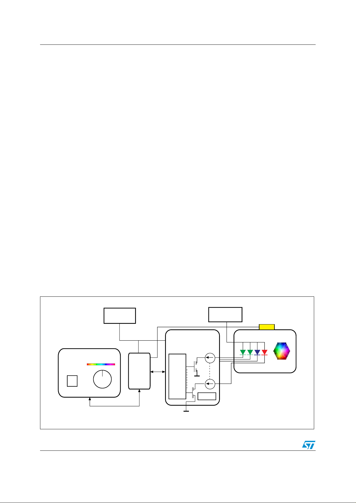
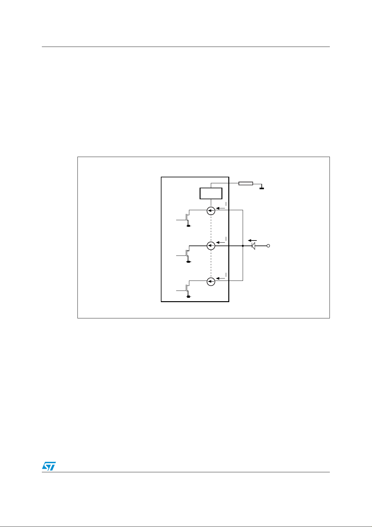
1 Driving concept for RGB LEDs
RGB refers to the three primary colors, red, green, and blue. Different colors can be
generated by controlling the power to each LED. In this application, the microcontroller
provides three software PWM signals (principle is described below in Chapter 4) for L ED
drivers STP04CM596 so the color can be regulated.
The STP04CM596 is a high-power LED driver with 4- bit shift register designed for power
LED applications. In the output stage, four regulated current sources provide 80-500 mA
constant current to drive high power LEDs.
Figure 2 shows the driving concept for RGB LEDs using an STP04CM596 LED driver. The
LED supply voltage is conn ected to anode s of RGB L ED and LEDs cathodes a re connected
to the ground through constant current sources. The supply voltage value is very important
due to the power dissipation on drivers (detail explanation is described in Chapter 5).
The value of the constant current is set by only one e xternal resistor for all the four driver
channels. The control unit in this application is a microcontroller, which sends data through
serial peripheral interface (SPI) to the shift registers inside STP04CM596. The data are
shifted bit by bit to the next driv ers in a cascade with falling edge of the clock frequency (the
maximum communication frequency for this drivers is 25 MHz). When all data are
transmitted to the drivers through SPI, the micro sets latch input terminal (LE) pin “log 1" to
rewrite the data to the storage registers and to turn on or off the LEDs. More details on
timings and features are available in Application Note AN2141 (refer to Chapter 11, point 3)
and Datasheet of the STP04CM596 (refer to Chapter 11, point 4).
Temperature protection is designed in order to protect LEDs and increase their lifetime.
A sensor (STLM20) is assembled close to the RGB LEDs and informs the microcontroller
about RGB LED temperature. If the tem perature is abov e its limit, the microcontroller
decreases LED brightness (LED power) through PWM signal.
An easy and user friendly hardware interface (potentiometers and b u ttons) w as de signed t o
demonstrate fe atures such as color set, brightness regulation, mode changes, etc.
Figure 2. Driving concept for RGB LEDs
IC supply
voltage
CONTROL PANEL
SPI
MODE
Micro
COLOR
STP04CM596
Control
and
logic
part
Constant
current
I - reg.
LED supply
voltage
Temperature sensor
Full color pixel
6/37
AI12675
Page 7
AN2531 How to drive many LEDs
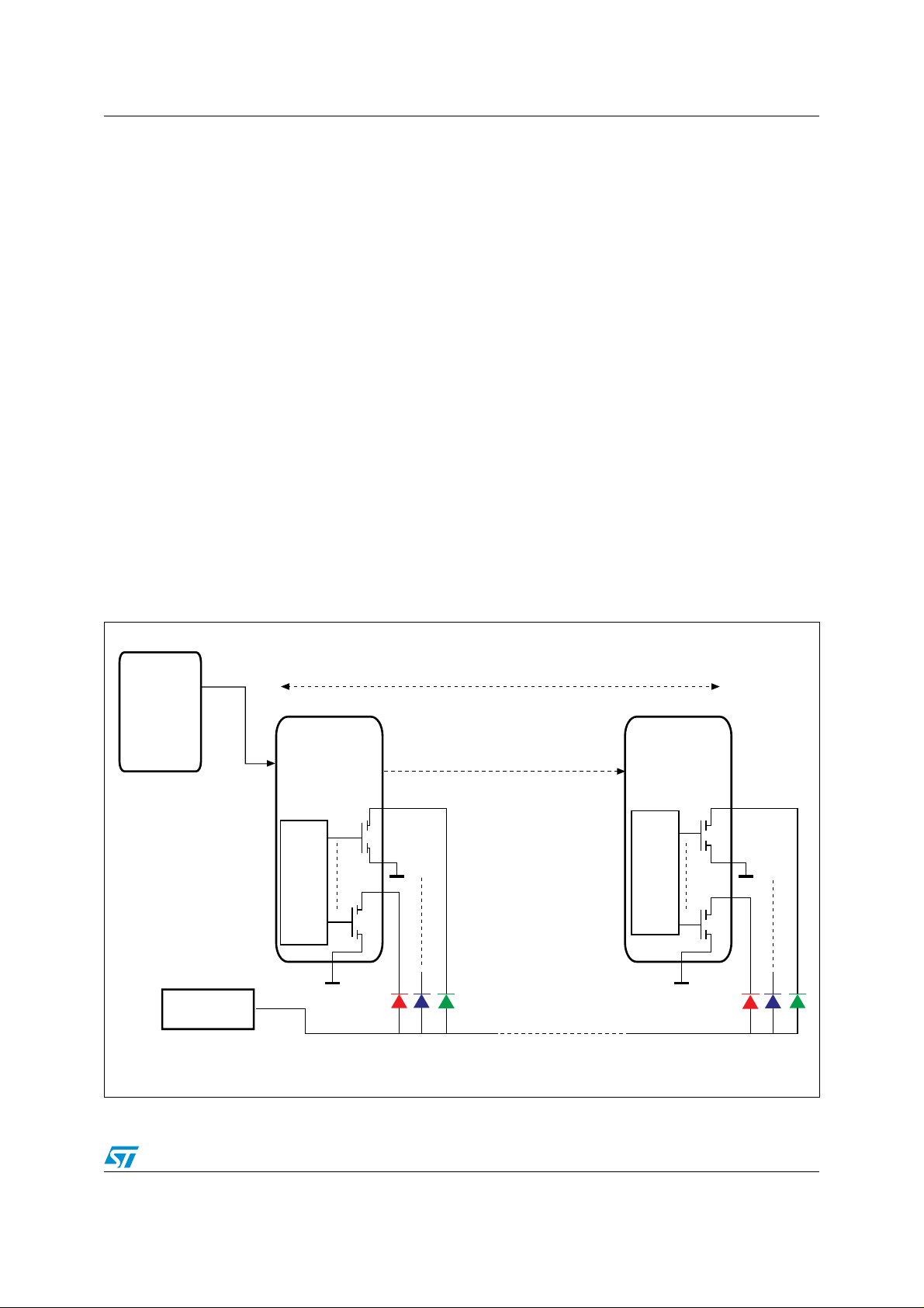
2 How to drive many LEDs
In several applications not only one RGB LED, but many of them must be driven. There are
at least two possible ways to drive many RGB LEDs using the STP04CM5 96 LED driver,
depending on the specific lighting application.
If the request is to control each RGB LED independently, a serial configuration (drivers in
cascade connection) must be used as shown in Figure 3. The data are sent thr ough all LE D
drivers via the SPI and then latched to the outputs. The main advantage is that current in
each channel can be regulated by software PWM modulation, which in fact means color
control of each RGB LED. The disadvantage of this solution is lower PWM resolution for a
higher number of RGB LEDs, because it needs time to send data to all drivers. More
information about this principle is described in Chapter 4: Color control - software
modulation.
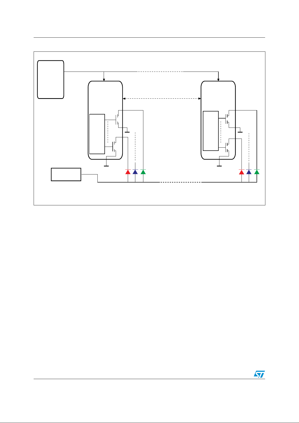
If the request is to build up a high power light with many LEDs of the same color, drivers can
be connected in parallel as shown in Figure4. Main advantages are a simpler solution and
better PWM resolution, because only four bits are sent through the SPI and it takes a short
time. Color is also regulated by software PWM signals as described in Chapter 4.
Note: It is also possible to mix serial and parallel config urations in order to provide se v eral diff erent
colors with high lighting power . For e xample , two diff erent colors using 10 RGB LEDs can be
implemented using two STP04CM596 connected in series and five such blocks connected
in parallel.
Figure 3. LED driver connection - serial configuration
SPI
Micro
STP04CM596
Control
and
logic
part
LED supply
voltage
Serial connection
SPI
STP04CM596
Control
and
logic
part
AI12687
7/37
Page 8
How to drive many LEDs AN2531
Figure 4. LED driver connection - parallel configuration
SPI
Micro
LED supply
voltage
STP04CM596
Control
and
logic
part
Parallel connection
STP04CM596
Control
and
logic
part
AI12676
8/37
Page 9
AN2531 How to set high current for LEDs
3 How to set high current for LEDs
The STP04CM596 is focused on driving high brightness and power LEDs and its output
constant current can be set between 80 and 500 mA. In case a LED with even higher
current is used, there is still a solution to control such LED using the STP04CM596. Thanks
to a common drain configuration, th e outputs can be connected together as shown in
Figure 5. This increases the performance and current capability of this driver. This
configuration allows driving the whole range of HB LEDs available on the market. For
example, this principle is also used in the STEVAL-ILL009V1 presented in this application
note, because the board has maximum current capability of 700 mA (2 channels x 350 mA).
Figure 5. Common drain configuration
STP04CM596
I-REG
R
ext
V
o
V
f
+ V
c
V
o
V
o
AI12677
9/37
Page 10

Color control - software modulation AN2531
4 Color control - software modulation
Software control modulation allows adjusting power to each channel of the STP04CM596
driver (i.e. LED brightness). Figure 6 explains the principle sho wing an example of how to
set an 8% duty cycle for red, 28% duty cycle for blue, 6 % duty cycle f or green and 98% duty
cycle for a fo urth LED. For one comp lete dimming cycle, the microcontroller sends a certain
number of “0”s and “1”s to each LED. First, the microcontroller sends four bits in “logical 1"
(i.e. 1111b or Fh) to the driver in order to turn ON all the output channels. Then
microcontroller sends the same data (1111) until an output should be turned OFF
(depending on desired preset color). (Each bit of the 4-bit frame controlling its
corresponding output.) In this example, it is output 3 with green LED (6% duty cycle
required). From that moment, the microcontroller keeps sending 1101. In the next step the
output 1 with red LED (8% duty cycle) should be turned OFF and so data frame changes to
0101. This frame is sent until output 2 with blue LED (28% duty cycle) should be turned OFF
and when the frame 0001 is used. Finally, the output 4 with another LED (usually second
green LED) is turned OFF with 98% duty cycle, which means than 0000 is being sent until
maximum time for one cycle is reached. After that, the entire period for all outputs can start
again.
Figure 6. Software brightness modulation
T
SW_PWM
1111 1111 or new data1101 0101 0001 0000
DATA
T SEND_DATA
Output 1
Output 2
Output 3
Output 4
LEVELS
t
8 % Duty Cycle
t
28 Duty Cycle
t
6 % Duty Cycle
t
98 % Duty Cycle
AI12678
The resolution of the LED dimming defines how many steps are possible to change the duty
cycle from 0% to 100% (e.g. 6-bit means 64 steps; 7-bit means 128 steps and so on). It is
obvious that it is preferred to design the control signal with a resolution as high as possible,
but several limitations should be taken into account. Limitations concern mainly the speed of
the serial communication interface inside the microcontroller (SPI) and the general
calculation power of the microcontroller. First, the general LED frequency should be
10/37
Page 11

AN2531 Color control - software modulation
selected. This value is recommended to be above 100 Hz in order to avoid flickering as at
100 Hz and above it is not detected by the human eye and is considered as a stable light.
Using Equation 1 and Equation 2, the resolution can be obtained as shown in Equation 3.
Equation 1
t =
SW_PWM
Equation 2
t
SEND_DATA
Equation 3
LEVELS
In order to have a good resolution, the time for sending data (t
as possible. In an ideal case, this time takes into account the number of sent bits and the
speed of the SPI clock (one bit is sent during one SPI period). As described in Figure 6, the
number of sent bits corresponds to the number of driven LEDs , therefore in Equat ion 4, the
number of driven LEDs is the same as number o f bits sent (BITS = LEDS).
Equation 4
t
SEND_DATA
=
BITS
f
SPI_CLK
1
f
SW_PWM
t
SW_PWM
=
LEVELS
×
SPI_CLK
1
tf
SEND_DATASW_PWM
SEND_DATA
BITSt
×==
) must be as short
The maximum number of used LEDs is (assumption BITS = LEDS):
Equation 5
LEDS
Note: The above calculation is only v alid only when the da ta are sent to the driv er throug h the SPI
without any delay. This means the data (BYTES) are sent thought the SPI and at the end of
this communication the next data (BYTES) are immediately sent, etc.
In case the data are sent through the SPI and then microcontroller executes some other
instructions (checking temperature , checking ADC in or der to set next PWM signal, et c.), the
period (t
resolution.
SEND_DATA
) for sending data is longer and it decreases the real maximum
=
11/37
1
LEVELStf
SPI_CLKSW_PWM
××
Page 12

Power dissipation AN2531
()(
)
(
)
+
+
5 Power dissipation
The maximum power dissipation can be calcula ted with ambient temperature and thermal
resistance of the chip. The thermal resistance depends on the type of package and can be
found together with maximum junction temperatur e in the datasheet. The maximum
allowable power consumption without a heatsink is calculated as follows:
Equation 6
T–T
P =
dmax
P
……. maximum power dissipation [W]
d max
T
……….…. ambient temperature [°C]
a
T
……... maximum junction temperature [°C]
j max
R
………. junction to ambient thermal resistance [°C/W].
thja
A high power RGB LED is in fact driven in linear mode with STP LED driver family. The
current flowing through each chann el of the LED drive r is const ant and so p o wer d issipation
depends on the voltage on each channel, which is the diffe rence between the su pply voltage
(DC bus) and the forward voltage drop on the LEDs. Therefore it is recommended to keep
the supply voltage as lo w a s possible, but alw ays abov e th e maxim um LED forward voltage.
Figure 7 shows the RGB LED connection to the driver . Total power dissipation in this case is
calculated using the following equation:
R
ajmax
thja
Equation 7
=
P
……….…….power dissipation on chip [W]
tot
I…………………constant LED current set by external resistor [A]
V
………………LED supply voltage [V]
c
V
………….red LED forward voltage [V]
f_red
V
….…….blue LED forward voltage [V]
f_blue
V
……....green LED forward voltage [V].
f_green
V–VI*2V–V*IV–V*IP
f_greenCf_blueCf_redCtot
12/37
Page 13

AN2531 Power dissipation
Figure 7. RGB LED configuration
STP04CM596
I-REG
R
ext
V
f_red
V
o
V
f_blue
V
o
V
f_green
V
o
V
f_green
V
o
V
c
AI12679
Note: Red, blue and green LEDs have different forward voltages ( refer to Chapter 2). In general,
the red LED has a lower forward voltage and therefore the pow er dissipat ion on the red LED
channel is the highest. There is quite simple wa y to de crease this pow er dissipation by using
a serial resistor with the red LED. Calculation example is shown in Section 9.1 and 10.1.
13/37
Page 14

Over-voltage protection AN2531
6 Over-voltage protection
6.1 Description
The maximum voltage on the output channels of STP04CM596 is 16 V. Any wire or PCB
track connection be tween LEDs and ST P04CM596 driver present s a parasitic inductance a s
shown in Figure 8. This parasitic inductance produces voltage spikes on the outputs of the
driver when the driver is t urning off the LEDs an d it can be danger ous for the STP04CM596
as it can exceed the maximum output voltage rating. Generally, higher current and higher
parasitic inductance (long cable) means higher volt age peaks. Therefore over voltage
protection is very important for high brightness LEDs in case of long connections between
the driver and LEDs.
Figure 8. Over-voltage on STP04CM596
4 V at 3 A
Temperature sensor
STP04CM596
Maximum output
voltage 16 V
Full color pixel
SPI
Control
and
logic
part
Over-voltage
Lp
Lp
Lp
Lp
AI12680
14/37
Page 15
AN2531 Over-voltage protection
6.2 Type of solutions
Figure 9 shows possible types of over voltage protection. The first solution proposes a
transil or a zener diode connected between each channel of the LED driver and ground.
Unidirectional transils with break down voltage lower than 16 V such as the SMAJ transil
family (refer to Chapter 11, point 5) can be used.
The second solution proposes to use a standard diode or Shottky diode as a freewheeling
diode. Diodes are connected betw een the LED supply v oltage (DC b us) and driver's channe l
and so limit the voltage on the channels.
The third solution is the most cost effective and uses only a single zener diode which
protects all channels. It can be used only if the connection bet ween the LED drive r and LED
cathodes is a quite short and if the connection between LED supply voltage and ano des is
long. This protection limits over voltage peaks on LED anodes.
Figure 9. Possible over voltage protections
STP04CM596
SPI
Control
and
logic
part
Maximum output
voltage 16 V
Transil
4 V at 3 A
3
21
Zener
diode
Lp
Temperature sensor
Full color pixel
Lp
D
Lp
Lp
Lp
4
Zener
diode
AI12681
15/37
Page 16

LED temperature protection AN2531
7 LED temperature protection
The STEVAL-009V1 was designed for high power RGB LEDs with a no minal power even
higher then ten watts . As the lifetime of LEDs significantly decreases with temperature, the
proper temperature management must be implemented to check and limit its maximum
values.
Two different temperature protections are used in this design as shown in Figure 10 - the
STLM20 temperature sensor and NTC (negative temperature coefficient) resistor. The
STEVAL-ILL009V3 uses an NTC resistor directly assembled on the aluminum LED board
(OSTAR projection module). The STEVAL-ILL009V4 has assembled the STLM20
temperature sensor in the middle of LEDs on the PCB. The microcontroller checks the
voltage from the sensor s and sets the correct output PWM signal on the OE pin of the LED
drivers. The microcontroller can increase the duty cycle of the PWM signal (0% duty cycle is
max bright and 100% duty cycle is no bright) or can turn OFF the RGB LED if over
temperature occurs. Software implementation is up to designers. Temperature protection
calculation using the STLM20 or NTC is presented in Chapter 8.5.2.
Figure 10. Temperature protection
STEVAL - ILL009V4 STEVAL - ILL009V3
Vc
ADC
STLM20 Micro
R
NTC
AI12682
16/37
Page 17

AN2531 STEVAL-ILL009V1 reference board
8 STEVAL-ILL009V1 reference board
STEVAL-ILL009V1 reference board shown in Figure 1 was designed to demonstrate how
high power and high brightness RGB LEDs can be driven and to confirm the principles
described in the paragraphs above.
This board has the following main features:
● Different LEDs as a load can be used (additional boards connected through 30 pin
connector)
● 8 LEDs with 350 mA can be driven (e.g. GOLDEN DRAGON module - STEVAL-
ILL009V4)
● 4 LEDs with 700 mA can be driven (e.g. OSTAR module - STEVAL-ILL009V3)
● LED over temperature protection using STLM20 or NTC resistor
● LED temperature limit set by software
● 3 A at 4 V DC/DC converter using L4973D3.3 f or user friendly input (8 - 30 V)
● Color regulation (manual / auto)
● Brightness PWM regulation with 64 levels using OE pin (dimming all LEDs)
● Red, Green, Blue individual tuning
● White color preset mode
● LED frequency = 100 Hz
● 64 Levels of brightness for each LED with software color control
● 262144 color variations (64 x 64 x 64)
● SW start up implemented (200 ms)
● Over voltage protection implemented using clamp schottky diodes (BAT46)
● 6 different light MODES available
● Input over voltage protection done by transil (SMAJ33A)
● Over temperature signalization
● I
connector for SW evaluation and change.
CC
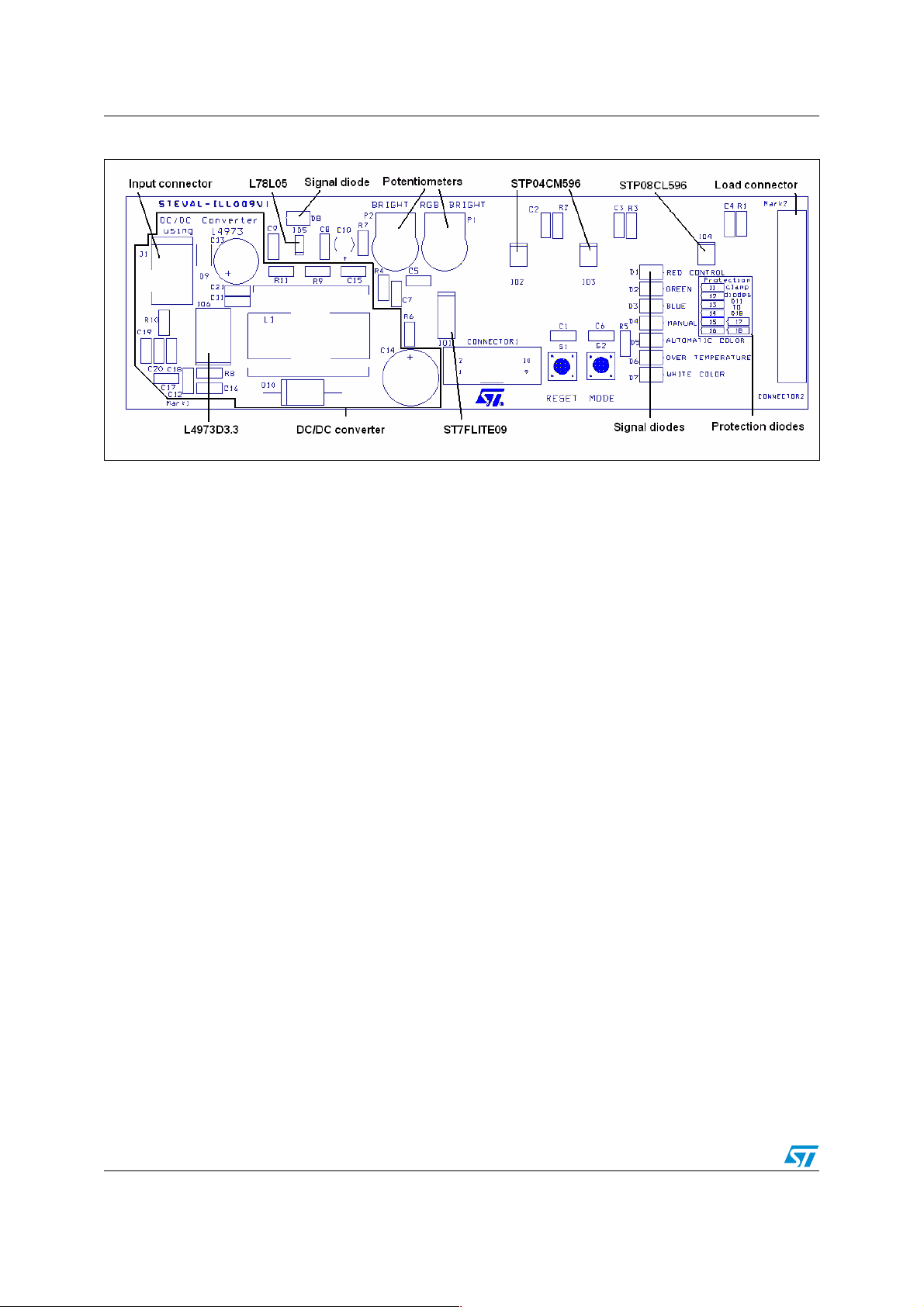
8.1 General description
Figure 11 shows components position on the STEVAL-ILL009V1. On the left side there is
DC/DC converter with L4973D3.3 (ref. toChapter 11, point 6) with power capability 3 A
at 4 V. The input voltage range is fr om 8 to 30 V and it is connect ed through input connecto r.
The L78L05 (ref. to Chapter 11, point 7) provides 5 V supply voltage for the microcontroller
and LED drivers (signal diode D8 is used to show connected power). Potentiometers P1 and
P2 are used to set brightness for all LEDs or tuning ea ch of them separately. High power
RGB LEDs are driven by STP04CM596 and STP08CL596 is used to control signal LEDs
(D1-D7) which are implemented to show which of the se v era l lighting modes is currently set.
30 pins load connector provides better flexibility, because different types of LEDs can be
connected to the same board. As an example two load boards with LEDs were designed STEVAL-ILL009V3 and STEVAL-ILL009V4.
17/37
Page 18
STEVAL-ILL009V1 reference board AN2531
Figure 11. Components position on the STEVAL-ILL009V1
8.2 Getting started
Getting started chapter briefly describes how to use the STEVAL-ILL009V1 as a step by
step guide in order to quickly start with the evaluation.
1. Connect LED board to the STEVAL-ILL009V1 reference board using the 30-pin load
connector2. STEVAL-ILL009V3 or STEVAL-ILL009V4 is LED boards.
2. Connect the supply voltage between 8 to 30 V on the board using J1 connector. The
power capability of the adapter must be higher then 14 W in order to have enough
energy for the application.
Note: The maximum channel current is set to 350 mA and so the LEDs and driver power
consumption is P
is approximately 80 % (P
= 4V x 0.35 mA x 8 = 11.2 W . The efficien cy of the DC/DC con v erter
LEDout
= 13.44 W). Considering the microcontroller and LED drivers
LEDin
themselves must be also supplied (consumption is less than 0.5 W) the total consumption is
~14 W and therefore the power capability of the adapter must be higher then 14 W in order
to have enough energy for the application.
3. If the application is supplied, the green LED (D8) is lighted ON. It shows that there is a
supply voltage for the micro and the drivers. Also LED D5 is turned ON at the start-up
as the Automatic Color Control mode is set. Colo r automatically changes from blue to
green, green to red and red to blue . During this mode, the brightness of all LEDs can be
changed by potentiometer P2, but the function of the potentiometer P1 is disabled in
this mode.
4. Press the button (S2) to change the mode. The next mode is White Color Control
mode. LED D7 is turned ON. The brightness of all LEDs can be changed by
potentiometer P2 and the function of the potentiometer P1 is disabled in this mode.
5. Press the button (S2) to set the next mode. It is Red Color Control mode. In this mode
the brightness for the Red LED can be changed by potentiometer P1. There are 64
levels of brightness implemented. LED D1 is turned ON and the potentiometer P2 has
the same function as in point 4 - changing the brightness of all LEDs.
6. Press the button (S2) to set brightness for the Green LED. In this mode the brightness
for the Green LED can be changed by potentiometer P1. LED D2 is turned ON. The
potentiometer P2 has again the same function - chang ing the brightness of all LEDs.
18/37
Page 19

AN2531 STEVAL-ILL009V1 reference board
Note: The brightness level of the RED light is set by previous mode and stor ed in the mem ory and
so the effect of the GREEN color is added to the RED one.
7. Press the button (S2) to set brightness for the Blue LED. In this mode the brightness for
the Blue LED can be changed by potentiometer P1. LED D3 is turned ON. The
potentiometer P2 has the same function - changing the brightness of all LEDs.
Note: The brightness levels o f the RED and GREEN lights were set b y pre vious modes and stored
in the memory and so the BLUE color is added to the RED and GREEN one.
8. The next mode (press button S2) is a Manual Color Control mode. It means the color
can be set as requested (going through predefined R-G-B curve) by the potentiome ter
P1. LED D4 is turned ON. The potentiometer P2 has the same function - changing the
brightness of all LEDs.
9. During all modes described above, LED temperature control is implemented. If
over temper ature occurs, th e brightness of all LEDs is decreased b y PWM signal on the
general OE/ pin (64 leve ls). The temperature is checked every 2.55 s and if it is still
above the limit, the d uty cycle of PWM is further increased (OE/ pin has a “not output
enable” function, i.e. higher the duty cycle lower the brightness and vice versa). The
maximum temperature o n the LED board is set to 50 °C for the GOLDEN Dr agon LEDs
and 72 °C for the O STAR Projection module. Note that th e higher t empera ture limit can
be very easily set by software.
10. How to demonstrate over temperature protection? Set full brightness by
potentiometer P2 in White Color Control mode and wait approximately 3 minutes with
STEV AL-ILL009V3 ( board with heatsink) o r 1½ minutes with STEVAL-ILL009V4 (board
without heatsink). Temperature on LEDs is increased and if the over temperature is
detected, LED D6 is turned ON and the PWM duty cycle is increased and the
brightness decreased overcoming the potentiometer setti ngs. The temperature of LED
board then should go down and if no over temperature is detect ed after the period of
time, the duty cycle is decreased again and normal operation is resumed.
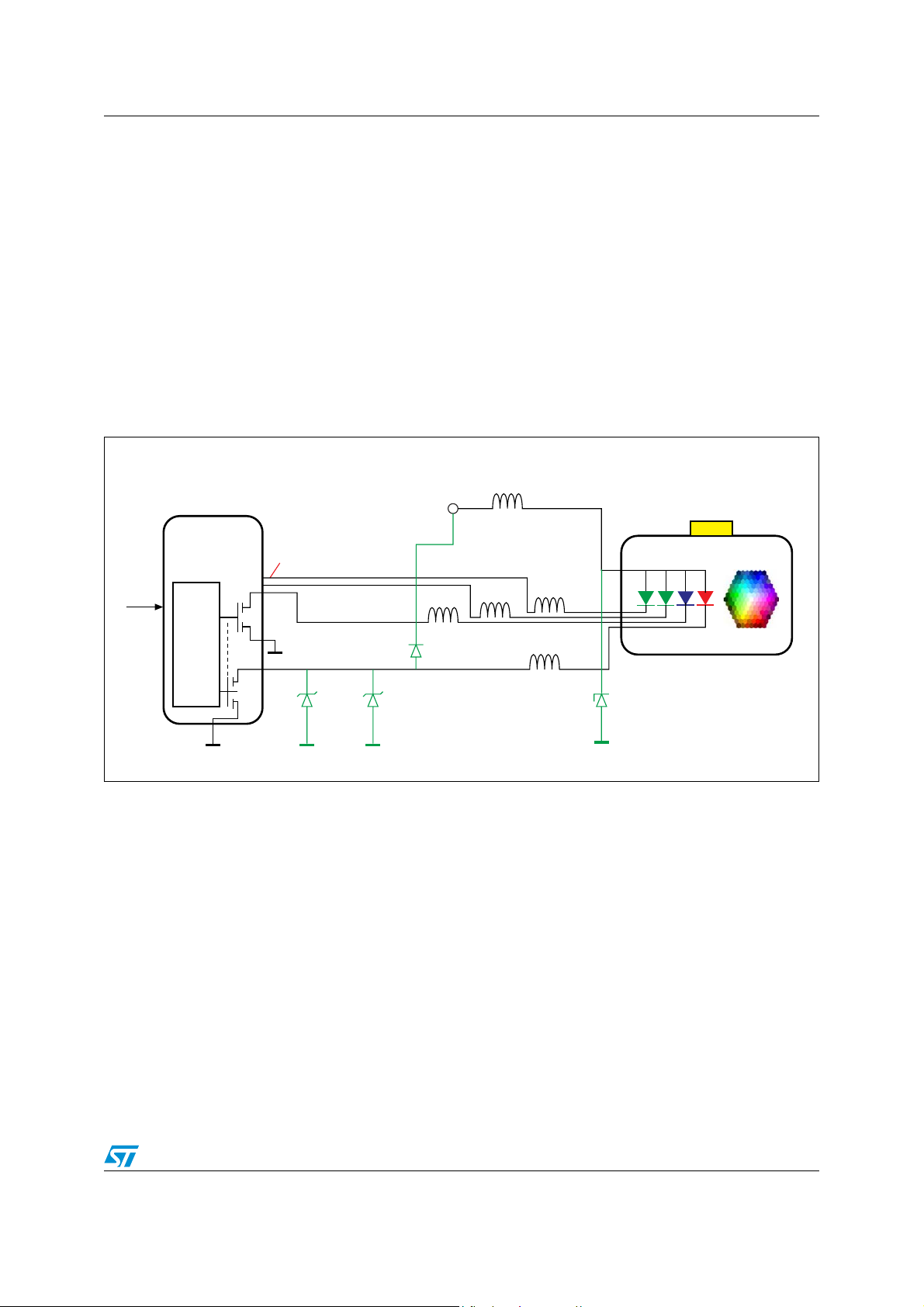
8.3 Schematic description
The STEVAL-ILL009V1 reference board schematic diagr am is shown in Figure 12 and
Figure 13. It is divided into two figures for easier understanding.
Figure 12 shows the components needed for LED driving. Resistors R2 and R3 set a
maximum constant current 350 mA f or each output channel of the STP04 CM596. Thanks to
this configuration, eight high brightness LEDs with the forward current 350 mA or 4 LEDs
with the forward current 700 mA (two outputs are in parallel) can be driven. The
STP08CL596 drives signal LED diodes with the constant current set to appr o ximately 8 mA.
The signal coming from the NTC resistor or STLM20 temperature sensor assembled in
additional board (load boards) is filtered b y a low-pass filter using capacitor C7 and resistor
R6.
Figure 13 shows the power sources for the application. A 12W DC-DC SMPS converter is
built on L4973D3.3 and design calculations are described in the datasheet (ref. to
Chapter 11, point 6) or in the AN938 (ref. to Chapter 11, point 8). The L78L05 is a linear
voltage regulator with output voltage set to 5 V used for microcontroller and driver s supply.
19/37
Page 20

STEVAL-ILL009V1 reference board AN2531
Figure 12. STEVAL-ILL009V1 schematics - LED drivers part
R1
CC
V
C4 100 nF
14
16
15
DD
V
SDO
R-EXT
GND1SDI2CLK3/LE4OUT05OUT16OUT27OUT3
IO4
13
/OE
3 KΩ
9
OUT712OUT611OUT510OUT4
8
STP08CL596
AI12671
CC
V
C3 100 nF
CC
V
C2 100 nF
IO3
IO2
IO1
15
16
DD
V
GND1GND2SDI3CLK
15
16
DD
V
GND1GND2SDI3CLK
16
Vss
V
2
1
14
R_ext
14
R_ext
DD
R3
9
12
13
11
NC
/OE
SDO
OUT210OUT3
/LE5OUT06OUT17NC
8
4
R2
9
12
13
11
NC
/OE
SDO
OUT210OUT3
/LE5OUT06OUT17NC
8
4
9
10
13
11
NC12NC
PA214PA115PA0
ICCCLK
ICCDATA
RESET3AIN04SCK5AIN26MOSI7CLKIN
8
NC
NC
PA7
220
STP04CM596
220
596
STP04CM
LI
ST7FLITE09
LED0
LED1
Vd
PROTECTION
1 BAT46
D12 B AT46
D1
R5 10 KΩ
CC
V
D13 B AT46
LED2
D14 B AT46
S2
LED3
D15 B AT46
C6
10 nF
SWITCH
CC
I
LED4
CONNECTOR1
1 2
3 4
5 6
7 8
9 10
INFORMATION SIGNALS
LED5
LED6
CC
V
D18 B AT46
D16 B AT46
D17 B AT46
CC
V
LED0 - RED LED CONTROL
LED1 - GREEN LED CONTROL
LED2 - BLUE LED CONTROL
LED3 - MANUAL COLOR CONTROL
LED4 - AUTOMATIC COLOR CONTROL
LED5 - OVER TEMPERATURE
LED6 - WHITE COLOR
Vd
30
Vd
29
Vd
28
Vd
27
NC
26
NC
25
CC
V
24
NC
23
Vo
22
NC
21
GND
20
19
GND
NC
18
NC
17
B2
16
B2
15
14
G2b
CONNCON ECTOR2
13
G2b
12
G2a
11
G2a
R2
10
R2
9
B1
8
B1
7
6
G1b
5
G1b
a
4
G1a
3
G1
R1
2
R1
1
R6 470
CC
V
C5
CC
V
Brightness
P1
10 KΩ
Color
100 nF
C1
10 nF
C1
S1
Switch
CC
V
20/37
C7
R4
4.7 KΩ
100 nF
P2
10 KΩ
Page 21

AN2531 STEVAL-ILL009V1 reference board
Figure 13. STEVAL-ILL009V1 power sources schematic
R11
C17
100 nF
STPS5L60
D10
C20
C2
6.2 kΩ
22 nF
C19
220 pF
C18
100 nF
V
CC
IO5 L78L05ACD
R9
1.3 kΩ
Vd
C15
100 nF
+
DMT2-149-3.8L
COILCRAFT
L1
R7
1
OUT
V
IN
V
8
D8
390
B
INHI
GND
GND
GND
GND
C8
5
7
6
3
2
0
C1
C9
Green LED
/
35 V
33 µF
100 nF
100 nF
IO6
R8
C21
C11
13
10
VFB
BOOT
L4973D3.3
SYNC
20
CC
V
9
8
CC
V
OSC
SS19V3.3
1
20 kΩ
100 nF
2
100 nF
OUT3OUT
GND
GND
GND
D
GN
18
GND
GND
GND
GND
INH
COMP
150 µF
17
16
15
14
7
6
5
4
11
12
C14
4700 µF / 10 V
R10
9.1 kΩ
AI12672
123
J1 CON3
FROM 8 UP TO 30 V
INPUT VOLTAGE
21/37
C12
100 nF
D9
2,7 nF
C16
+
+
C13
SMAJ33A-TR
470 µF /35 V
Page 22

STEVAL-ILL009V1 reference board AN2531
8.4 Bill of materials (BOM)
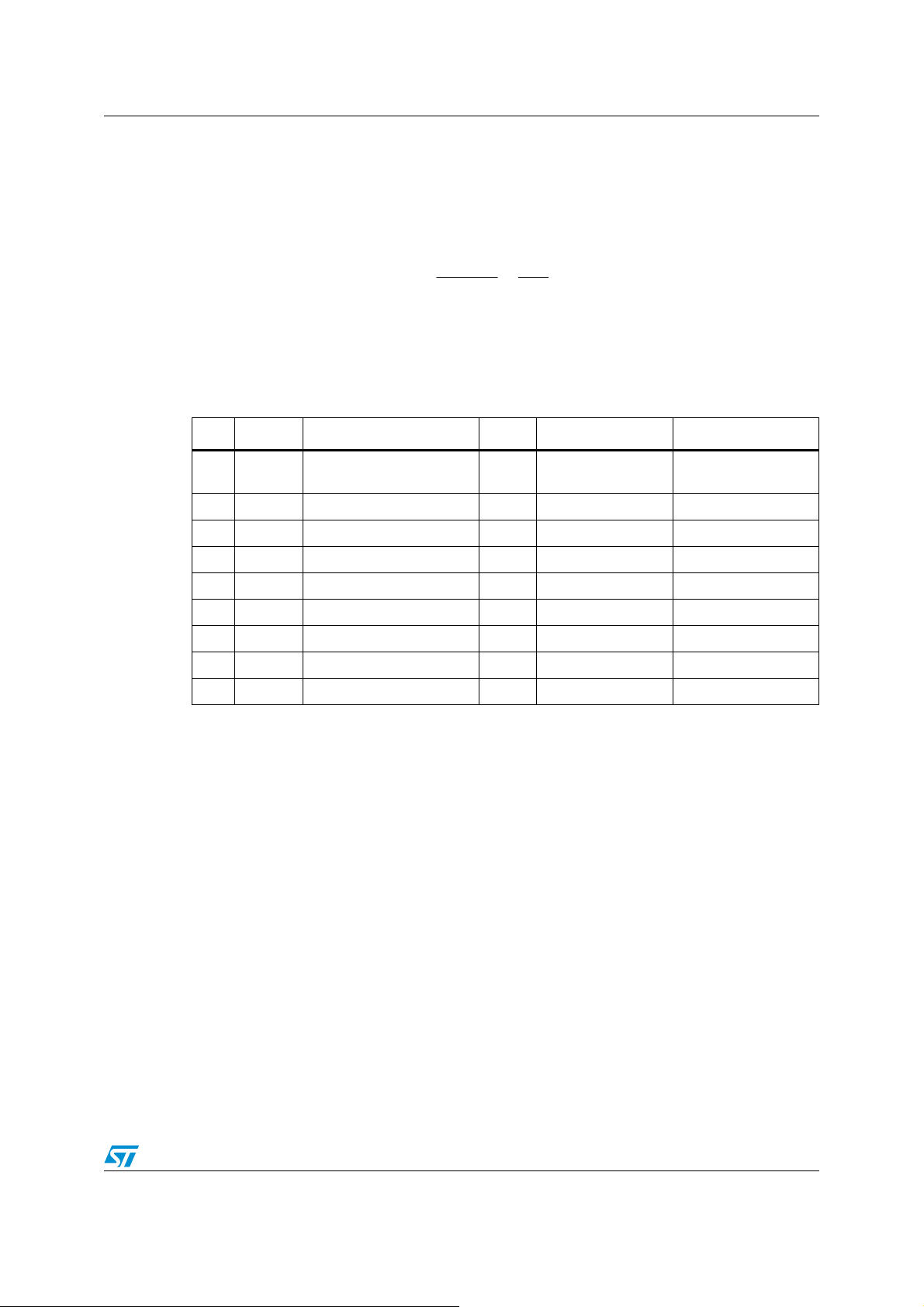
Table 1. BOM - STEVAL-ILL009V1
Item Qty Reference Part Note Ordering code
1 1 CONNECTOR1 I
CC
10 PIN
2 1 CONNECTOR2 CON 30 PIN
3 2 C1, C6 10 nF Ceramic SMD1206
413
C2, C3, C4, C5, C7, C8, C9, C11, C12,
C15, C17, C18, C21
100 nF Ceramic SMD1206
5 1 C10 33 µF / 35 V Electrolytic
6 1 C13 470 µF / 35 V Electrolytic
7 1 C14 4700 µF / 10 V Electrolytic
8 1 C16 2,7 nF Ceramic SMD1206
9 1 C19 220 pF Ceramic SMD1206
10 1 C20 22 nF Ceramic SMD1206
11 7 D1, D2, D3, D4, D5 , D6, D7 Red LED SMD LED 1206
12 1 D8 Green LED SMD LED 1206
13 1 D9 SMAJ33A-TR ST - Transil SMAJ33A-TR
14 1 D10 STPS5L60 ST - Diode STPS5L60
15 8 D11, D12, D13, D14, D15, D16, D17, D18 BAT46 ST - Schottky diode BAT46JFILM
16 1 IO1 ST7FLITE09 ST - Microcontroller ST7FLITE09Y0M6
17 2 IO2, IO3 STP04CM596 ST - LED driver STP04C596XTTR
18 1 IO4 STP08CL596 ST - LED driver STP08CL596TTR
19 1 I O5 L78L05 ST - Voltage regulator L78L05ACD
20 1 IO6 L4973D3.3 ST - DC/DC converter L4973D3.3
21 1 J1 CON3 Input connector
22 1 L1 150 µH COILCRAFT Inductor DMT2-149-3.8L
23 2 P1, P2 10 kΩ Pot. with ax is
24 1 R1 3 kΩ SMD resistors 1206
25 2 R2, R3 220 SMD resistors 1206
26 1 R4 4.7kΩ SMD resistors 1206
27 1 R5 10 kΩ SMD resistors 1206
28 1 R6 470 Ω SMD resistors 1206
29 1 R7 390 Ω SMD resistors 1206
30 1 R8 20 kΩ SMD resistors 1206
31 1 R9 1.3 kΩ SMD resistors 1206
32 1 R10 9.1 kΩ SMD resistors 1206
33 1 R11 6.2 kΩ SMD resistors 1206
34 2 S1, S2 SWITCH Switch
22/37
Page 23

AN2531 STEVAL-ILL009V1 reference board
8.5 Design calculation
8.5.1 LED supply voltage
In order to have low power dissipation on STP04CM596 LED drivers it was chosen to have
LED supply voltage 4 V. The maximum current flowing through LEDs is 2.8 A (0.35 A x 8).
Therefore L4973D3.3 DC-DC converter with output power capability 12 W - 4 V at 3 A was
designed. The output voltage is calculated in Equation 8:
Equation 8
R
6.2
11
RR
+
911
3.3–4
=×==
1.3KΩ
3.3
VV
=
dF
Where:
V
……. Converter feedback input - > 3.3 V
F
V
…… LED supply voltage --> 4 V
d
From Equation 9 below resulting R9 = 1300 Ω (R11 is chosen 6.2 kΩ)
Equation 9
V–V
RR
119
V
Fd
F
8.5.2 Temperature protection
Using STLM20 temperature sensor
The STLM20 is a precise analog temperature sensor f or low current app lications. It oper ates
over a –55 to 130 °C (G rade 7) or –40 to 85 °C (Grade 9) temperature range. The power
supply operating range is 2.4 to 5.5 V. The accuracy of the STLM20 is ± 1.5 °C, at an
ambient temperature of 25 °C. More information about the STLM20 is described in the
datasheet (refer to Chapter 11, point 9).
A simple linear transfer function, with good accuracy near 25 °C is expressed as:
Equation 10
o
–3
If the sensor temperature is 50 °C, the output volt age is 1.263 V (resulting from
Equation 10). This analog voltage is then sensed by the 8-bit ADC with an input voltage
range 0 to 5 V inside the microcontroller. This number is used by software to limit the
temperature. The software also includes the table with pre-calculated int eger numbers for
temperatures of 60, 70 and 80 °C and so it is very easy to change temperature limits (see
Table 2).
Note: Temperature limit set to 50 °C was chosen in order to demonstrate temperature limitation
feature (it takes a long time to heat LEDs assembled on heatsink to high temperature). In
final application higher temperatur e limit can be set according the LEDs used and their
maximum operating temperature.
1.263V1.85285010–11.791.8528VTC–11.79mV/V
=+××=+×°=
23/37
Page 24

STEVAL-ILL009V1 reference board AN2531
Table 2. Temperature limit setting using STLM20
Temperature [°C] Sensor voltage [V] ADC integer number
50 1.263 65
60 1.145 59
70 1.027 53
80 0.909 47
Using NTC resistor on the OSTAR module
Figure 10 shows a voltage divider using resistor R and NTC resistor to obtain a voltage in
function of temperature . Resistor was ch osen R = 4700 Ω and the calculat ed sensor v oltage
and ADC integer number according used NTC resistance for 50, 60, 70 and
80 °C using following equation:
Equation 11
NTC
×=
RNTC
+
Note: V
CC
= 5 V.
VV
CCsensor
The software also includes a look-up table with pre-calculated integer numbers for 50, 60,
70 and 80 °C and so it is very easy to change the temperature limit (see Table 3).
Note: The software implemented in the STEVAL-ILL009V1 sets the integer number to 65. This
means that the temperature is limited to 50 °C for the board using STLM20 (STEVALILL009V4) and to 72 °C for the board using OSRAM module with NTC resistor (STEVALILL009V3).
Table 3. Temperature limit setting using NTC
Temperature [°C] NTC resistance [kΩ] Sensor voltage [V] ADC integ er number
50 3.5 2.13 109
60 2.5 1.73 89
70 1.7 1.32 68
80 1.3 1.08 55
24/37
Page 25

AN2531 STEVAL-ILL009V1 reference board
8.5.3 SW PWM frequency calculation
In order to have a correct PWM signal on each output, it is necessary to always send data
after the same time. This means that the t
explained in Figure 6). The ST7FLITE09 microcontroller has a 12-bit auto-reload ti mer used
to generate a constant time base for data sending. It is set to 156 µs and so after each 156
µs period, the data are sent. Resolution is 6 bits and therefore 64 brightness levels are
available. One period of the SW dimming signal is:
Equation 12
Equation 13
f
SW_PWM
Note: Some applications often require a PWM frequency higher than 100 Hz (even 100 Hz is
observed as a still color without any flickering) and also a PWM resolution higher than 6-bit
(64 LEVELS). Figure 14 shows the waveform of SPI clock frequency that explains why the
6-bit resolution of the PWM signal and frequency 100 Hz was designed. The time for
sending data is 156 µs, but the SPI communication takes only 4 µs (8 bit times 0.5 µs - SPI
clock is 2 MHz) and the rest (152 µs) is software execution due to many features as
temperature protection, lighting modes, ADC reading, etc. As shown, there is still room to
improve the SW PWM resolution by decreasing time for data sending. Software
improvements that d emonstrate higher resolutio ns are already under de velopme nt ev en with
existing hardware only done by code optimization.
1
t
SW_PWM
SEND_DATA
SEND_DATASW_PWM
==
value must be always same (as
–6
9.984ms1015664tLEVELSt
=××=×=
1
×
=
3–
109.984
Hz 100.16
Figure 14. Send data time diagram
25/37
Page 26
STEVAL-ILL009V1 reference board AN2531
8.6 Software
The software is written in C language with several modules, but the most important files for
proper operation of the STEVAL-ILL009V1 reference board are the following:
● main.c
● blink.c
● pwm_ar_timer_12bit.c
● spi.c
● adc_8bit.c
Note: The final code has slightly less than 1.4 KBytes and it will fit the ST7FLITE09 memory.
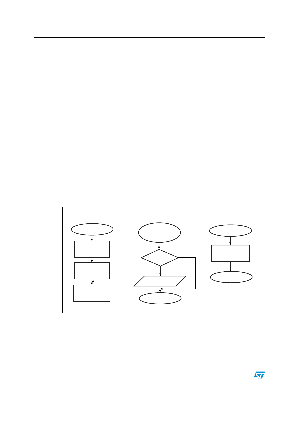
Main programming flowchart is shown in Figure 15. The program starts in main.c and
initializes the microcontroller functions such as RC oscillator calibration, ports initialization,
PWM AR timer setting for ti me base generation and SPI initialization (SPI clock frequency).
Afterwards, the interrupts are enabled and the program runs in a never-ending loop in
function blink.c.
Basically three interrupts can occur. First, an AR timer overflo w interrupt, which generates a
time base 156 µs for the software dimming in order to have precise brightness regulation.
When this interrupt occur , the program checks if all data have been already sent through
SPI or not. If not the data ar e missed a nd the pr ogr am w aits for next interrupt (156 µs), b ut it
is only some kind of backup protection. The second int errupt is a SPI interrupt, which
informs that data (single byte) ha v e been alread y sent. The last interrupt is an external input
interrupt, which detects that button was pressed.
Figure 15. Main program flowchart
FLOWCHARTS for the RGB color control board
MAIN
Microcontroller
initialization
Enable
interrupts
Main procedure
BLINK
AR_Timmer_OF
interrupt after
each 156 µs
All DATA
are sent
Y
Time base
ON
Return
SPI interrupt
N
All DATA are sent
YES
Return
AI12683
The heart of the software is a blink function running in a never-ending loop. In the start part
(Figure 16), the program waits until a PWM interrupt occurs during synchronization the n the
Counter_SW value is incremented. Genera lly, Counter_SW represents the number of levels
for the software PWM modulation and in this case it is 64 (6-bit resolution) (described in
detail in Chapter 4). The Brightness value set by potentiometer P2 is con verted by the ADC
to a value between 0 and 64 in each SW PWM period (each 10 ms / 100 Hz) and this value
sets the PWM brightness on the Output Enable (OE) pin.
26/37
Page 27
AN2531 STEVAL-ILL009V1 reference board
The next block checks the temperature every 2.55 seconds. This time is considered fast
enough because, due to its inertia, there is no need to check the temperature any faster. If
its value is higher than the limit, the PWM duty cycle is increased (0% duty cycle is full bright
and 100% is no light) by one step. Therefore, the light is absolutely turned OFF after 163.2
seconds (64 levels tim es 2.55). If the temperature is lower then the limit, the PWM duty
cycle starts decreasing down to maximum brightness (0%) and normal operation.
Time3 = 200 ms is used as a stabilization time for the DC-DC conv erter and linear regulator .
The output capacitors C10 and C14 (Figure 13) should be charged first to avoid resetting
the microcontroller (low voltage detector) and the flickering application due to the high load.
At the end, the high power RGB LEDs are turned ON after 200 ms. This time delay occurs
only once, when the application starts.
Figure 16. Blink function flowchart - first part
Start
BLINK
Time base 156 µs
?
Y
Counter_SW ++
Time1 = 10 ms
64 x 156 µs
N
1
N
Y
Read brightness
from potentiometer
P2 (digital value
from ADC)
Time1 = 0
1
Time1 = 2.55 s
255 x 64 x156 µs
N
Time3 = 200 ms
20 x 64 x156 µs
2
Y
Time2 = 0
Temperature
Limit > measured
value
N
Increase bright
about 1 step
Time3 = 0
Startup = OFF
Negative
temperature
Y
coeficient
Decrease bright
about 1 step
AI12684
Figure 17 shows the second part of the blink function - the brightness setting (based on
value read on P2 in first pa rt) and mode selection (mode is selected b y pres sing b utto n S2).
MODE 1, MODE 2 and MODE 3 sets the brightness for the red, g reen and b lue LEDs where
the brightness level (0 to 64) is obtained from the potentiometer P1 after each SW PWM
period (10 ms).
R, G & B elements could be set in single step with MODE 4 and MODE 5. This means the
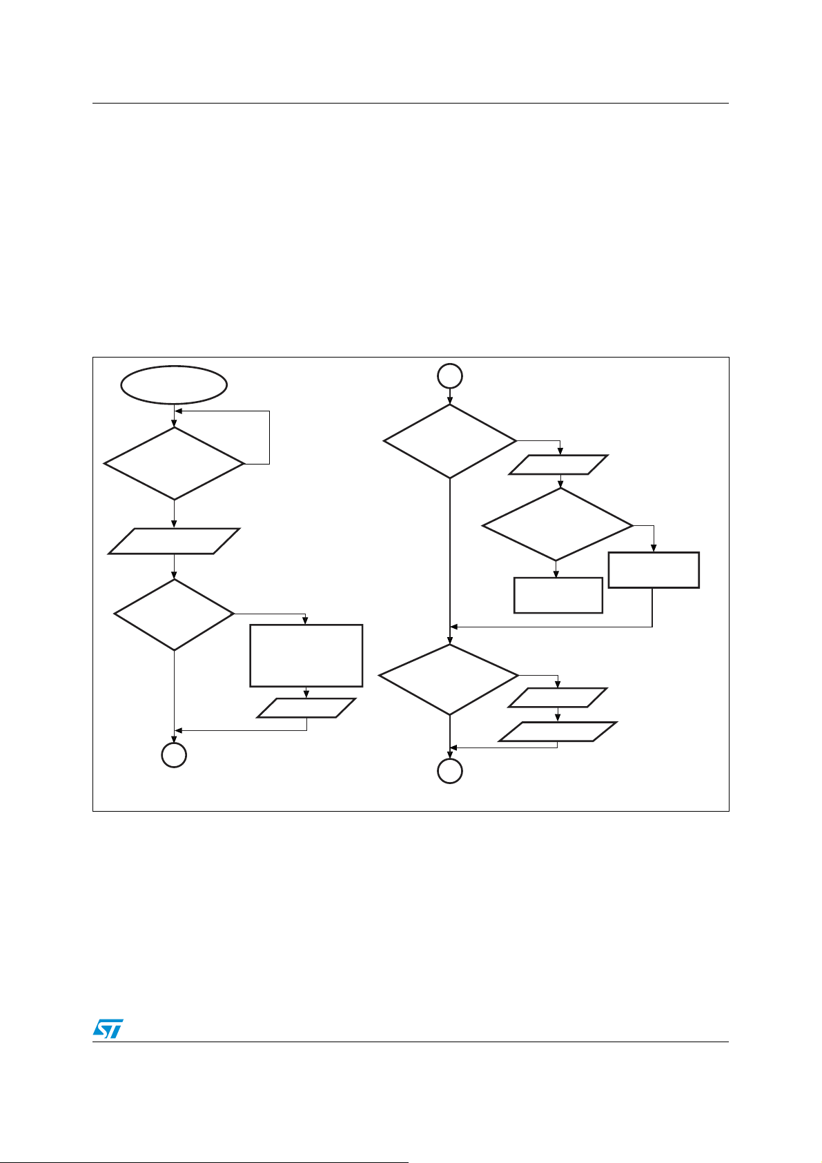
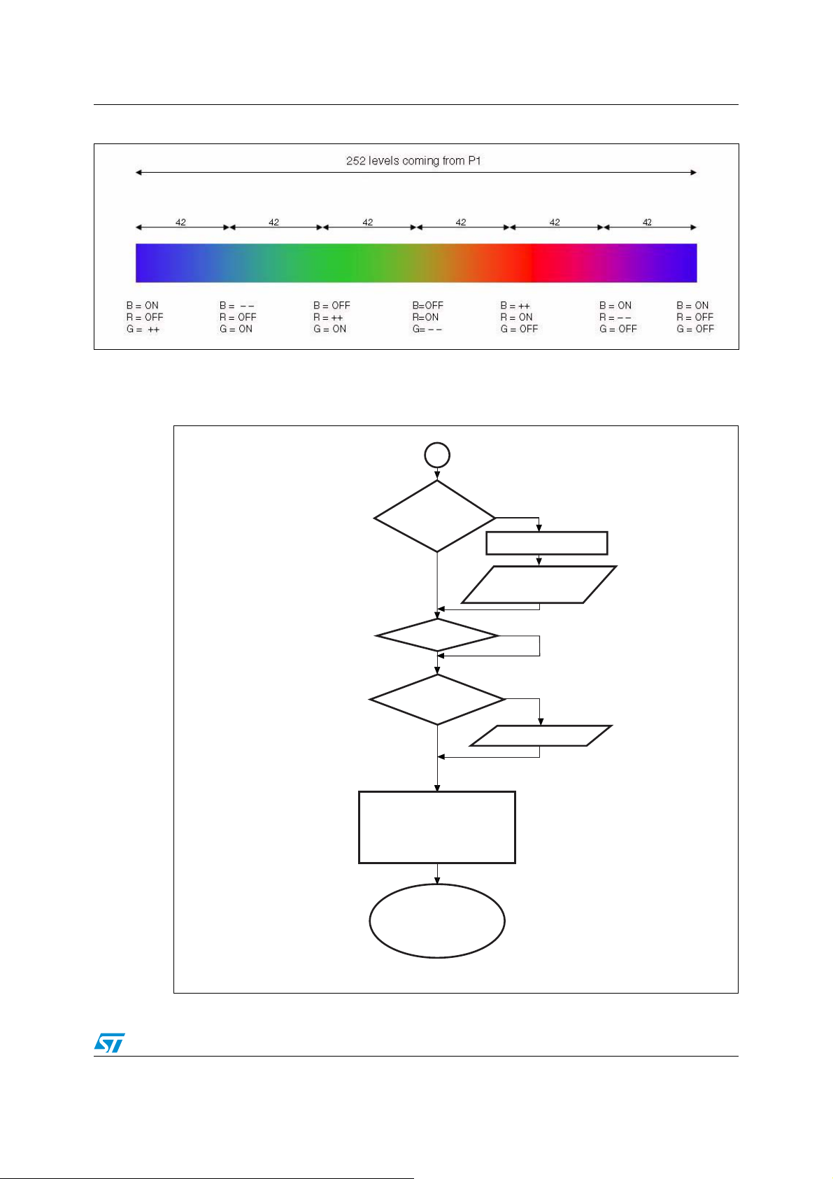
color is moving on a predefined curve as indicated in Figure 18. The difference between
MODE 4 and MODE 5 is that MODE 4 is controlled by potentiometer P1 and MODE 5 is
working automatically (simulating the P1 input). Figure18 shows how it works. The integer
27/37
Page 28

STEVAL-ILL009V1 reference board AN2531
number coming from ADC (potentiometer P1) has r ange from 0 to 252. This r ange is divided
to six segments where always just one color is changed and two are constant ( ON or O FF).
Blue color is set if the potentiometer is in the left side (0 from ADC), because B = ON (blue),
R = OFF (red) and G = OFF (green). If the value from ADC is increased to 42, the PWM of
green color is decreased. In case ADC has value 42 the green is fully turned ON together
with blue and red is OFF. The ADC value fr om 43 to 84 increases blue color (light is going
down) and if ADC has value 84 only green LED is O N. In this wa y it is possible to mo v e light
through all basic colors. MODE 5 represents automatic color changing. The principle of the
automatic color change is similar to manual color control, because the color level is not
adjusted by potentiometer P1 (0-252), but automatically using the 156 µs time base
generated by the auto-reload timer.
Note: In order to demonstrate the best lighting effects, the application automatically starts in
MODE 5 - automatic color changing mode.
Figure 17. Blink function flowchart - second part
2
Set bright
PWM on OE pin
Mode changed
N
MODE 1
N
MODE 2
N
Y
Set starting
conditions
Y
Set RED bright
Set DATA_blink1
Set DATA_blink2
Y
Set GREEN bright
Set DATA_blink1
Set DATA_blink2
3
MODE 3
N
MODE 4
N
MODE 5
N
Y
Set BLUE bright
Set DATA_blink1
Set DATA_blink2
Y
Set manual color
Set DATA_blink1
Set DATA_blink2
Y
Startup = ON
Set auto color
Set DATA_blink1
Set DATA_blink2
Overtemperature
3
28/37
4
AI12685
Page 29
AN2531 STEVAL-ILL009V1 reference board
Figure 18. Manual color modulation
The last mode implemented is MODE 6, which is the simplest one - all the LEDs are turned
ON, which produce the pure white color. Figure 19 describes this last part.
Figure 19. Blink function flowchart - third part
4
Y
MODE 6
N
Default
Counter_SW = 64
N
Write to the SPI
Register
SPIDR = DATA_blink1
SPIDR = DATA_blink2
Return
Blink procedure
starts again
Set WHITE color
Set DATA_blink1
Set DATA_blink2
Y
Counter_SW = 0
AI12686
29/37
Page 30
STEVAL-ILL009V3 Load board AN2531
9 STEVAL-ILL009V3 Load board
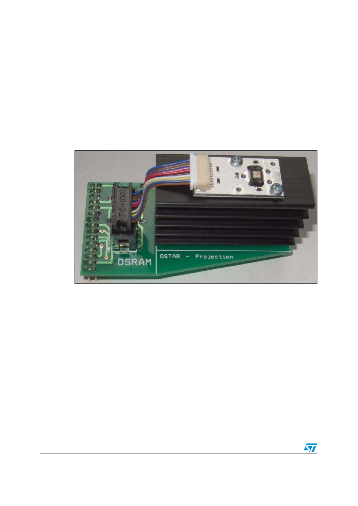
The STEVAL-ILL009V3 demo board is shown in Figure 20. This board should be connected
through the 30-pin connector to the ST EVAL-ILL009V1 control board to be able to sho w t he
light effect with the board. The OSTAR projection module (ref er to Chapter 11, point 1), used
as light source, has a maximum forward current 700 mA. The NTC resistor is directly
assembled on the OSTAR module. As the power of the module is above 10 W the heatsink
had to be designed in order to k ee p the t emper a ture in r a nge . Th e bigg est advantage of the
OSTAR module is that red, green and blue LEDs are in the same package, very closely
assembled and therefore color effect is better than with three separate LEDs.
Figure 20. STEVAL-ILL009V3
9.1 Schematic description
The schematic of the STEVAL-ILL009V3 is shown in Figure 21. As described, the constant
current flowing through each channel is set to 350 m A , but because 700 mA is needed to
drive the OSTAR module, two outputs are connected in parallel (Figure 21). Resistor R4
represents together with the NTC resistor the voltage divider for the temperature sensing
(described in detail in Chapter 8.5.2). The software has a preset temperature limitation 50
°C for Golden Dragon LEDs using STLM20 temperature sensor, which means a voltage of
1.263 V on the ADC. The NTC has a resistance of 1588 Ω at72 °C and the voltage coming
from resistor divider to the ADC is exactly 1.263 V. So, the default temperature limit for the
OSTAR module is 72 °C, but it can be v ery easy changed by software. The HB LEDs are
supplied from the DC/DC converter 4 V at 3 A.
The maximum green and b lue LEDs f orw ard v oltage is 4 V, but the red f orw ard v oltage is 3.4
V. If 3.4 V is around red LED, the rest of the supply voltage (4 V) must be on the driver
(0.6 V) causing a power loss and therefore the design includes the connection of resistors
R1, R2 and R3 to decrease power dissipat ion on LED drivers and move these losses to th e
resistors.
30/37
Page 31
AN2531 STEVAL-ILL009V3 Load board
=
=
Equation 14
Equation 15
9.2 Bill of materials
Table 4. STEVAL-ILL009V3 bill of materials
Item Quantity Reference Part Note Ordering code
1 1 OSTAR projection module
2 1 Cable with connector 10 lines cable SHR-10V-S-B -> JST
3 1 Heatsink SEMIC Trade 8150/50/N
4 1 Connector1 10 pin s
5 1 Female Connector1 10 pins
6 1 Connector2 30-pin connector
=
R
diss
F_RED_MAXdR
V
R
I
RED_LED
0.6
===
0.7
OSRAM OSTAR
Projection Module
0.6V3.4–4V–VV
0.85Ω
LE ATB A2A
71 R1 0
8 2 R2, R3 1.5 Ω Through-hole 0.6 W
9 1 R4 4.7 kΩ Through-hole 0.6 W
31/37
Page 32

STEVAL-ILL009V3 Load board AN2531
Figure 21. STEVAL-ILL009V3 schematic diagram
R3
R2
1.5
1.5 Ω
5 Ω
1R12
R1
10
U_r = Ud - Uf_red_max = 4 - 3.4 = 0.6 V
ICC
123456789
CONNECTOR1
R_diss = U/I = 06 / 0.7 = 0.85 => 0.75 Ω
R2 = R3 = 1.5 Ω R2 || R3 = 0.75 Ω
R1
0
0
R4
47 kΩ
5 V
4700 Ω
9
10
7
3
G1
G1
8
4
5
6
B1
R2
G1
b
a
B1
a
G1
R2
b
15B216
11
12
13
14
17
G2
B2
a
G2
a
NC
G2
b
G2
b
22
20
19
18
21
23
NC
GND
NC
Vo
NC
GND
24
Vcc
28
29
27
30
26
25
NC
Vd
Vd
NC
Vd
Vd
NTC 1.263 V for 72 ˚C
CONNECTOR2ICC
32/37
R_ntc (72 ˚C) = 1588 Ω
AI12673
Page 33

AN2531 STEVAL-ILL009V4 Load board
10 STEVAL-ILL009V4 Load board
The STEVAL-ILL009V4 demo board is shown in Figure 22. This board is an option to the
STEVAL-ILL009V3. As a light source, there are four Golden Dragon LEDs (refer to
Chapter 11, point 2) used with a maximum forward current of 350 mA. As described in
Chapter 8, the STEVAL-ILL009V1 can d rive eight Golden Dr agon LEDs. To demonstrate the
driving capability of the STP04CM596, only four LEDs are used on the load board. In fact,
this means that one STP04CM596 driver is not used. The STLM20 temperature sensor is
assembled in the middle of the LEDs to protect against overheating (as described in
Section 8.5).
Figure 22. STEVAL-ILL009V4
33/37
Page 34

STEVAL-ILL009V4 Load board AN2531
=
=
10.1 Schematic description
The schematic of the STEVAL-ILL009V4 is shown in Figure 23. The temperature limitation
of the Golden Dragon LEDs is set to 50 °C on this boar d. Similar to the STEVAL-ILL009V3,
resistors R4, R5 and R6 are used to decrease the power dissipation on LED driver. The
resistor value is calculated using the following equation:
Equation 16
Equation 17
10.2 Bill of materials
Table 5. STEVAL-ILL009V4 bill of materials
Item Quantity Reference Part Note Ordering code
1 2 G1a, G1b L TW5SM HZ-3
2 1 R1 LRW5SM HY-1
3 1 B1 LBW5SM FX-3
=
R
F_RED_MAXdR
V
R
I
RED_LED
1.4
0.35
===
Dragon Green LED
1.4V2.6–4V–VV
4Ω
OSRAM Golden
OSRAM Golden
Dragon Red LED
OSRAM Golden
Dragon Blue LED
Q65110A5876
Q65110A4386
Q65110A4396
4 1 C7 100 nF / 50 V Ceramic SMD1206
5 3 R4, R5, R6 10 Ω Through-hole resistor
6 1 IO7 STLM20 ST Temperature sensor STLM20W87F
7 1 Connector2 30-pin connector
34/37
Page 35

AN2531 STEVAL-ILL009V4 Load board
Figure 23. STEVAL-ILL009V4 schematic diagram
Vd
30
used (R4||R5||R6)
Ω
=> 3.3
Ω
1
3
2
Vo
NC
GND
V+
IO5
GND
4
5
Temperature sensor
CC
V
C7
100 nF
STLM20
29
28
27
26
25
24
23
22
21
20
19
18
17
16
15
14
13
12
11
10
9
8
7
6
5
4
3
2
1
Vd
Vd
Vd
NC
NC
CC
V
NC
Vo
NC
GND
GND
NC
NC
B2
B2
G2b
G2b
G2a
G2a
R2
R2
B1
B1
G1b
G1b
G1a
G1a
R1
R1
AI12674
2
CONNECTOR
C
IC
R4 10
R = U_r / I = 1,4 / 0.35 = 4
U_r = U_d - U_f_red = 4 - 2.6 = 1.4 V
R5 10R5 10
R6 10R6 10
R1 G1a G1b B1
35/37
Page 36

Reference and related materials AN2531
11 Reference and related materials
1. OSRAM Opto Semiconductors, LE ATB A2A, Datasheet of OSTAR Projection Module
http://www.osram-os.com
2. OSRAM Opto Semiconductors, Datasheet of GOLDEN Dragon LEDs
http://www.osram-os.com
3. STMicroelectronics, AN2141, LEDs Array Reference Board Design
http://www.st.com
4. STMicroelectronics, STP04CM596, 4-bit constant current for power-LED sink driver,
data-sheet; http://www.st.com
5. STMicroelectronics, SMAJ, Transil, Datasheet; http://www.st.com
6. STMicroelectronics, L4973D3.3, 3.5 A step down switching regulator, Datasheet;
http://www.st.com
7. STMicroelectronics, L78L05, Positive voltage regulators, Datasheet; http://www.st.com
8. STMicroelectronics, AN938, Designing with L4973, 3.5 A high efficiency DC-DC
converter http://www.st.com
9. STMicroelectronics, STLM20, Ultra - low Current 2.4 V precision analog temperature
sensor, Datasheet; http://www.st.com.
12 Revision history
Table 6. Document revision history
Date Revision Changes
3-May-2007 1 Initial release.
36/37
Page 37

AN2531
Please Read Carefully:
Information in this document is provided solely in connection with ST products. STMicroelectronics NV and its subsidiaries (“ST”) reserve the
right to make changes, corrections, modifications or improvements, to this document, and the products and services described herein at any
time, without notice.
All ST products are sold pursuant to ST’s terms and conditions of sale.
Purchasers are solely res ponsibl e fo r the c hoic e, se lecti on an d use o f the S T prod ucts and s ervi ces d escr ibed he rein , and ST as sumes no
liability whatsoever relati ng to the choice, selection or use o f the ST products and services described herein.
No license, express or implied, by estoppel or otherwise, to any intellectual property rights is granted under this document. If any part of this
document refers to any third pa rty p ro duc ts or se rv ices it sh all n ot be deem ed a lice ns e gr ant by ST fo r t he use of su ch thi r d party products
or services, or any intellectua l property c ontained the rein or consi dered as a warr anty coverin g the use in any manner whats oever of suc h
third party products or servi ces or any intellectual property contained therein.
UNLESS OTHERWISE SET FORTH IN ST’S TERMS AND CONDITIONS OF SALE ST DISCLAIMS ANY EXPRESS OR IMPLIED
WARRANTY WITH RESPECT TO THE USE AND/OR SALE OF ST PRODUCTS INCLUDING WITHOUT LIMITATION IMPLIED
WARRANTIES OF MERCHANTABILITY, FITNESS FOR A PARTICUL AR PURPOS E (AND THEIR EQUIVALE NTS UNDER THE LAWS
OF ANY JURISDICTION), OR INFRINGEMENT OF ANY PATENT, COPYRIGHT OR OTHER INTELLECTUAL PROPERTY RIGHT.
UNLESS EXPRESSLY APPROVED IN WRITING BY AN AUTHORIZED ST REPRESENTATIVE, ST PRODUCTS ARE NOT
RECOMMENDED, AUTHORIZED OR WARRANTED FOR USE IN MILITARY, AIR CRAFT, SPACE, LIFE SAVING, OR LIFE SUSTAINING
APPLICATIONS, NOR IN PRODUCTS OR SYSTEMS WHERE FAILURE OR MALFUNCTION MAY RESULT IN PERSONAL INJ URY,
DEATH, OR SEVERE PROPERTY OR ENVIRONMENTAL DAMAGE. ST PRODUCTS WHICH ARE NOT SPECIFIED AS "AUTOMOTIVE
GRADE" MAY ONLY BE USED IN AUTOMOTIVE APPLICATIONS AT USER’S OWN RISK.
Resale of ST products with provisions different from the statements and/or technical features set forth in this document shall immediately void
any warranty granted by ST fo r the ST pro duct or serv ice describe d herein and shall not cr eate or exten d in any manne r whatsoever , any
liability of ST.
ST and the ST logo are trademarks or registered trademarks of ST in various countries.
Information in this document su persedes and replaces all information previously supplied.
The ST logo is a registered trademark of STMicroelectronics. All other names are the property of their respective owners.
© 2007 STMicroelectronics - All rights reserved
STMicroelectronics group of compan ie s
Australia - Belgium - Brazil - Canada - China - Czech Republic - Finland - France - Germany - Hong Kong - India - Israel - I taly - Japan -
Malaysia - Malta - Morocco - Singapore - Spain - Sweden - Switzerland - United Kingdom - United States of America
www.st.com
37/37
 Loading...