

Page 1

AN2530
Application note
Solution for 150 W half bridge resonant DC-DC converter
Introduction
This application note describes a 150 W Half bridge resonant DC-DC converter. This type of
SMPS is highly attractive due to its high achievable efficiency, very low noise and compact
size.
Resonant converters are among the least common SMPS topologies. There are several
reasons why they are not often used, but we will not discuss these reasons in this
application note. However, it is worth noting that the resonant topologies have undeniable
advantages over the "hard switching" topologies. The very high achievable efficiency of over
90% and up to 95% is very common, as well as their low generated noise due to ZVS (zero
voltage switching) and resonant energy transfer.
Other related advantages derived from these converters are their compact size due to their
need for smaller power switches (Power MOSFETs usually), smaller transformers, and less
generated heat (the lower losses are a part of this). Less heat means a smaller heat sink
and a longer life for power components.
If the necessary care is taken in the design phase, the results are very good and the typical
issues normally associated with these topologies are avoided.
ST's L6598 half bridge driver has been chosen for this design. Please refer to the L6598
datasheet for full specifications and capabilities, or to other documentation, application
notes and books where it is used, in order to have the best picture of this design. All
references are provided in Figure 7.
This application note concentrates only on the power aspects, because as already
mentioned, there are excellent guides for the driver (aside from the datasheet) as well as
application notes for SMPS in general, magnetics, topologies, etc.
October 2007 Rev 1 1/13
www.st.com
Page 2

Contents AN2530
Contents
1 Functional overview . . . . . . . . . . . . . . . . . . . . . . . . . . . . . . . . . . . . . . . . . 3
2 Operational frequencies . . . . . . . . . . . . . . . . . . . . . . . . . . . . . . . . . . . . . . 6
3 Transformer and resonant components . . . . . . . . . . . . . . . . . . . . . . . . . 7
3.1 Transformer . . . . . . . . . . . . . . . . . . . . . . . . . . . . . . . . . . . . . . . . . . . . . . . . 7
4 Converter's protection schemes, overcurrent, overvoltage . . . . . . . . . 7
5 Full load, normal operation waveforms . . . . . . . . . . . . . . . . . . . . . . . . . 9
6 Conclusion . . . . . . . . . . . . . . . . . . . . . . . . . . . . . . . . . . . . . . . . . . . . . . . . 11
7 References . . . . . . . . . . . . . . . . . . . . . . . . . . . . . . . . . . . . . . . . . . . . . . . . 12
8 Revision history . . . . . . . . . . . . . . . . . . . . . . . . . . . . . . . . . . . . . . . . . . . 12
2/13
Page 3
AN2530 Functional overview
1 Functional overview
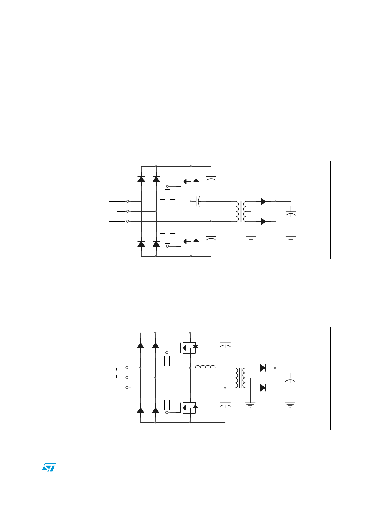
The simplest way of describing the functioning of a resonant converter is to compare it with
a non-resonant type. Typically a "normal" half bridge transformer is connected to the
principal DC bus through a capacitive divider network that creates a "false" ground to feed
one of the transformer's ends (Figure 1). In this way, the transformer is fed with a voltage
that swings (from the transformer's point of view) from zero to negative, negative to zero,
zero to positive, then back to zero (therefore repeating the cycle).
The mains DC bus is connected as noted in Figure 1 for 110 V
or 220 Vac. The operation
ac
is quite straightforward alternating the turn-on of each transistor.
Figure 1. SMPS half bridge simplified schematic
3
220VAC
110VAC
D3D4D1
D2
Q1
1
C3
2
3
1
Q2
C1
C2
1 5
T1
4 8
D5
6
D6
C4
+
The resonant variation for this type of converter places an "external" inductor to cause a
resonance between the capacitive divider network and the external inductor (Figure 2),
which sums up to the already present leakage inductance of the main transformer.
These components are the ones that require most of the care for this variation of the
converter. Nevertheless, remember that every aspect of the design stage has an impact on
the overall behavior of the converter.
Figure 2. Resonant SMPS half bridge simplified schematic
3
220VAC
110VAC
D3
D4
D1
D2
Q1
1
L1
2
3
1
Q2
2
C1
1 5
T1
4 8
C2
D5
6
D6
C4
+
Ta bl e 1 gives the BOM (Bill of materials) for this converter. Most of the capacitors do not
have an operating voltage, as they operate in low voltage. As for the driver, any voltage
3/13
Page 4

Functional overview AN2530
greater than or equal to 16 V is acceptable. The construction details of L1 and Tr1 are
discussed later.
Table 1. Bill of materials (BOM)
Qty. Ref. Part Qty. Ref. Part Qty. Ref. Part
1 AC 220 V
2 Cac1 1 nF/400 V 2 C26b 4700 pF / 2 KV R18 10 KΩ
Cac2 1 nF/400 V C26a 4700 pF / 2 KV R23 10 KΩ
1 C1 220 µF / 400 V 1 DC 24VDC 1 R10 20 KΩ
1 C4 1 µ 1 D1 W08G 1 R11 100 KΩ
1 C8 47 µF 1 D2 STPS20H100CT 2 R13 15
3 C10 100 nF 1 D3 1N4148 R15 15
C12 100 nF 1 D4 18 V 1 R17 39 KΩ
C20 100 nF 1 L1 51 µ 4 R19d 1
1 C11 1 nF 2 Q2 STP8NM60N R19c 1
2 C15 220 p Q1 STP8NM60N R19b 1
C13 220 p 1 R2 150 KΩ/2 W R19a 1
1 C14 0.22 µ 1 R3 10 1 R21 3.6 KΩ
1 C16 100 n 1 R4 150 KΩ 2 R25 1 KΩ
3 C17 33 n 1 R5 7.5 KΩ R22 1 KΩ
C18 33 n 2 R8 27 KΩ 1 R24 1.2 KΩ
C23 33 n R6 27 KΩ 1 Tr1 Transformer
3 C19c 470 µ 1 R7 6.8 KΩ 1 U1 L6598
Conn. 1 C22 0.47 µ R16 10 KΩ
ac
C19b 470 µ 6 R9 10 KΩ 1 U2 PC817
C19a 470 µ R12 10 KΩ 1 U3 TL431
1 C21 82 n R14 10 KΩ
Refer to Figure 3 for the full electrical schematic of this converter.
4/13
Page 5

AN2530 Functional overview
Figure 3. Converter’s full electrical schematic
1
2
DC
24VDC
1
3
C20
100nF
+
C19c
470µ
+
C19b
470µ
+
C19a
470µ
D4
STPS20H100CT
91311
TransformerSMPS
Tr1
7
6
4
2
D3
1N4148
C18
C17
33n
C23
D2
1N4148
D1
1N4148
D4
18V
R14
R3
10
R2
150K/2W
C8
47µF
1
3
1
2
MainDC
360VDC
10K
23
1
Q1
STP8NM60N
*
15
R13
Cp
100n
C12
100nF
15
16
HVG
Vboot
Vs
12
U1
+
OPOut
OPIn-
567
R8
27K
R7
6.8K
22n
1 2
L1
51µ
Q2
STP8NM60N
23
R16
1
R15
15
14
Out
OPIn+
4
R6
27K
C10
100nF
7.5K
R4
150K
R5
8
10
11
EN1
LVG
GND
RfMin
RfStart
2
22n
Current sensing
resistor
10K
Css
Cf EN2
3 9
network.
R18
1
L6598
C13
220p
R23
10K
C22
R25
1K
R22
1K
R21
3.6K
4
R19d
1
10K
1nF
10K
0.22µ
220p
39K
R12
R10
20K
1
R19c
1
R19b
1
R19a
C11
C4
1µ
R9
10K
C14
C15
R17
C21
PC817
U3
U2
2 1
3
C16
100n
R11
100K
This capacitor must be placed just below U1, directly
connected to Vs (pin 12) and Gnd (pin 10).
*
0.47µ
82n
TL431
R24
1.2K
3
2 1
C26b
4700pF / 2KV
C26a
4700pF / 2 KV
C1
220µF/400V
+
3
Dac
1.5A Bridge
2
4
-+
1
Cac2
1n
Cac1
1n
1
2
ONN PWR 2-H
P1
5/13
Page 6

Operational frequencies AN2530
2 Operational frequencies
Figure 3 shows a gray area with a note "optional". This rectifying stage is not really
necessary as it was done for testing and measuring purposes.
More explanations and clarifications are provided as we go through this design.
Much of the basis for this application note was taken from another ST application note,
mainly AN1660 (ZVS resonant converter for consumer application using L6598 IC), which is
a 180 W ZVS resonant converter. As stated in AN1660 (ZVS resonant converter for
consumer application using L6598 IC) you must "choose" some operational parameters that
are recalculated after real component values have been chosen. Only your experience with
this kind of SMPS can guide you.
For this case the following values have been chosen:
● F
● F
● F
The frequency values have been chosen keeping in mind that 300 kHz (F
to the driver's maximum operational frequency. Therefore, we leave the converter much
"room" to change its operational frequency (via the feedback) so the regulation does not
suffer because of a range that is too restrictive.
= 300 kHz
start
= 70 kHz
min
= 35 kHz
r
) is quite close
start
The calculations for Rf
below:
Equation 1
Equation 2
Recalculating F
min
& F
Equation 3
Equation 4
(R11) and Rf
min
Rf
Rf
start
-------------------------------------------------
start
with actual values of R
F
F
start
start
min
1.41
–()Cf•
F
startFmin
--------------------------
min
Rf
1.41
---------------------------- - F
Rf
startCf
(R6); Cf is C13 (220 pF) in our case, are shown
1.41
----------------------- -
F
minCf
1.41
minCf
•
91.56 KΩ==
•
27.27 kΩ==
fmin
64.09 kH z==
•
min
& Rf
237.4 kHz=+=
(∼ 100 kΩ)
(∼ 27 kΩ)
:
start
6/13
Page 7

AN2530 Transformer and resonant components
3 Transformer and resonant components
In order to avoid the majority of the most difficult problems related to resonant converters,
great care must be taken in the design of those components whose primary task is to
transfer the energy from the rectified line to the load. These components are the
transformer, external inductor, capacitor divider network and the power switches.
Several "methods" and approaches have been taken into account in order to calculate the
power transformer and the external inductor (refer to Section 7: References at the end of
this application note). AN1660 forms the basis for this application note and provides
calculations for this objective.
The objective of this application note is to take a closer look at the power stage, so that just
the final results for the transformer and the external inductor are shown. However, it is
important to notice that the transformer's type (material, size and shape) plays one of the
main roles in any converter. For resonants, the coil type is important also.
Ta bl e 2 gives transformer and coil data. Litz wires have been used.
3.1 Transformer
● Brand: Epcos
● Type: ETD34
● Material: N67
Table 2. Tr1 Transformer’s windings details
Turns Wires Wire's diameter [mm]
Primary 50 14 0.2
Secondary 14 38 0.2
Aux. 3 1 0.2
4 Converter's protection schemes, overcurrent,
overvoltage
Overcurrent and overvoltage protection features can be added easily thanks to the pins of
the L6598 controller. In this section we show how to calculate these values according to the
operational parameters chosen.
Again, refer to AN1660 (ZVS resonant converter for consumer application using L6598 IC)
or use your own "method" to calculate the peak current. You should expect to be at the
maximum at L1 (as well as transformer's primary) and take a safety margin (10% more for
example). In this case, the maximum current should be 1.8 A, so we set the maximum
current to 2 A.
7/13
Page 8

Converter's protection schemes, overcurrent, overvoltage AN2530
According to the L6598 datasheet there is a constant voltage of 2 V at pin 2 (Rf
), so this
start
voltage can be used to set the opamp's inverting input (pin 6) to 0.4 V through the R6 & R7
divider network.
The inverting input of internal opamp is set to 0.4 V, so 0.4 V/2 A = 0.2 Ω.
A set of 1 Ω/0.25 W resistances was chosen to be readily available and by paralleling them
we get 0.25 Ω/1 W, which "generates" 0.25 Ω*2 A = 0.5 V at maximum current.
Then, we have to choose the values for R17 & R18 (a resistor divider network) to get the
0.4 V at Pin 7 (OPin+), R17 = 39 kΩ and R18 = 10 kΩ in our case.
Concerning feedback, regulation is achieved by means of varying the driver's frequency. A
heavier load determines a lower operational frequency and the contrary is true for a lighter
load. Frequency is changed by varying the current at pin 4 (Rf
). As previously stated,
min
R11 defines the maximum operational frequency and R10, R12 and optocoupler's internal
resistance (that varies according to the current supplied to the load) set the actual operating
frequency.
8/13
Page 9

AN2530 Full load, normal operation waveforms
5 Full load, normal operation waveforms
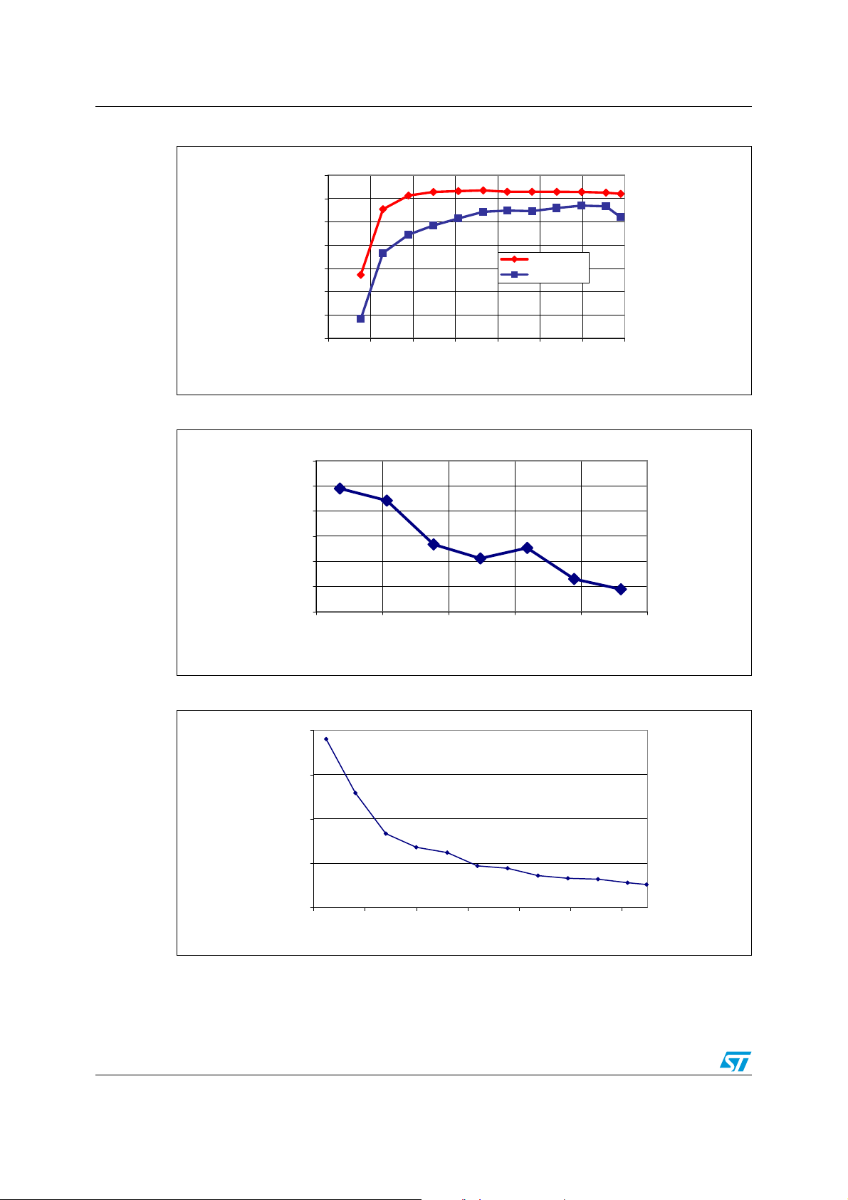
Figure 4 shows the normal full load operation waveforms for this converter.
Channels 1 and 2 are V
at Q2 and Q1 respectively. Notice that the voltage level at Q1
g
(upper MOSFET), is up to 370 V due to the charge pump inside the driver.
Channel 3 is the resonant current flowing through L1, measured with a hall effect probe.
There is a lack of symmetry probably caused by the hand-wound transformer and coil. The
major contributor to this should be the non-symmetric primary winding for the transformer
that imposes different loads as current flow changes direction at the primary.
Channel 4 is the resonant voltage at C18.
Figure 4. Operating waveforms at full load
● Measurement conditions
– Vin = 355 V
– Vout = 23.7 V
@ DC Main bus
DC
, 6.35A (~150 W)
DC
As previously stated in the introduction, this type of converter has some very good
characteristics, one of which is the very high efficiency, typically over 90%, that is easily
achieved with resonant, very low RF and EMI produced due to ZVS.
Figure 5 shows the efficiency curve against the output power and against input voltage
(Figure 6). Notice that there are two curves (Figure 5), the upper one is the efficiency curve
for this converter, as you can see in the schematic in Figure 3 . The other one is the same
converter connected after a PFC circuit. This one uses ST's L4981A as its primary driver,
provides 355 V
and up to 200 W. The application note AN628 appears in Section 7:
DC
References and is referred to in the conclusion.
9/13
Page 10
Full load, normal operation waveforms AN2530
Figure 5. Efficiency vs. Pout
95
90
85
80
75
Efficiency [%]
70
65
60
10 30 50 70 90 110 130 150
Pout [W]
Eff.
Eff. with PFC
Figure 6. Efficiency vs. Vin
92.4
92
91.6
91.2
90.8
Efficiency [%]
90.4
90
350 360 370 380 390 400
Vin [Vdc]
Figure 7. Switching frequency vs output power
250
200
150
Switchinf Freq. [KHz]
100
50
20 40 60 80 100 120 140
Pout [W]
10/13
Page 11

AN2530 Conclusion
Figure 8. Thermograph
ºC
D2
Q1, Q2
Tr1
The converter is working at full load in the thermograph in Figure 8. Notice that the hottest
spot is near the rectifier double diode (D2). The hot lines (white ones) are the dc out filtering
capacitors that are being heavily heated by D2 due to the board's position. The transformer
is working "cool" as well as the Power MOSFET transistors.
It is important to notice that Q1 and Q2 are working in the 50 ºC range. Originally the board
was assembled with bigger transistors, therefore the smaller ones can be used in this
application and gain in efficiency (almost 20% gain for light loads). They are easier to drive
and cheaper which means that you don't have to "oversize" these (as is usually done in
other converter topologies).
6 Conclusion
As already mentioned, a certain degree of attention must be exercised with resonant
converters because energy transfer is directly related to this phenomenon. The benefits are
substantial and include low emi and rf noise, high efficiency, overall cooler operation, no
need for "over sized" power components to prevent failure from spikes, etc., as well as other
advantages if designed carefully. As you can see, the load regulation of this one is very
good.
It is remarkable that all these measurements and tests have been performed without any
forced ventilation. The heatsink provided for the power transistors is very modest,
considering the SMPS's power, so it would be easy to avoid any heat sink by designing a
suitable copper area for SMD transistors (i.e. DPAK).
The designer will notice that since the power factor for this converter is not good, therefore
it is better to connect the converter after a PFC, such as the one with L4981 that has been
used to do some of these measurements. It is normal that the power factor is low due to the
"spike" nature of this converter's drawn current. If observed with an oscilloscope, a series of
spikes can be seen.
11/13
Page 12

References AN2530
7 References
● High frequency switching power supplies, theory & design.
● Closing The Feedback Loop. Lloyd H. Dixon Jr. Unitrode©
● Transformer and inductor design for optimum circuit performance. Lloyd H. Dixon Jr.
Unitrode©
● L6598 Datasheet
● AN1673, L6598 off-line controller for resonant converters.
● AN1660, ZVS Resonant converter for consumer application using L6598 IC.
● AN628, Designing a high power factor switching preregulator with the L4981
continuous mode.
8 Revision history
Table 3. Document revision history
Date Revision Changes
25-Oct-2007 1 Initial release
12/13
Page 13

AN2530
Please Read Carefully:
Information in this document is provided solely in connection with ST products. STMicroelectronics NV and its subsidiaries (“ST”) reserve the
right to make changes, corrections, modifications or improvements, to this document, and the products and services described herein at any
time, without notice.
All ST products are sold pursuant to ST’s terms and conditions of sale.
Purchasers are solely responsible for the choice, selection and use of the ST products and services described herein, and ST assumes no
liability whatsoever relating to the choice, selection or use of the ST products and services described herein.
No license, express or implied, by estoppel or otherwise, to any intellectual property rights is granted under this document. If any part of this
document refers to any third party products or services it shall not be deemed a license grant by ST for the use of such third party products
or services, or any intellectual property contained therein or considered as a warranty covering the use in any manner whatsoever of such
third party products or services or any intellectual property contained therein.
UNLESS OTHERWISE SET FORTH IN ST’S TERMS AND CONDITIONS OF SALE ST DISCLAIMS ANY EXPRESS OR IMPLIED
WARRANTY WITH RESPECT TO THE USE AND/OR SALE OF ST PRODUCTS INCLUDING WITHOUT LIMITATION IMPLIED
WARRANTIES OF MERCHANTABILITY, FITNESS FOR A PARTICULAR PURPOSE (AND THEIR EQUIVALENTS UNDER THE LAWS
OF ANY JURISDICTION), OR INFRINGEMENT OF ANY PATENT, COPYRIGHT OR OTHER INTELLECTUAL PROPERTY RIGHT.
UNLESS EXPRESSLY APPROVED IN WRITING BY AN AUTHORIZED ST REPRESENTATIVE, ST PRODUCTS ARE NOT
RECOMMENDED, AUTHORIZED OR WARRANTED FOR USE IN MILITARY, AIR CRAFT, SPACE, LIFE SAVING, OR LIFE SUSTAINING
APPLICATIONS, NOR IN PRODUCTS OR SYSTEMS WHERE FAILURE OR MALFUNCTION MAY RESULT IN PERSONAL INJURY,
DEATH, OR SEVERE PROPERTY OR ENVIRONMENTAL DAMAGE. ST PRODUCTS WHICH ARE NOT SPECIFIED AS "AUTOMOTIVE
GRADE" MAY ONLY BE USED IN AUTOMOTIVE APPLICATIONS AT USER’S OWN RISK.
Resale of ST products with provisions different from the statements and/or technical features set forth in this document shall immediately void
any warranty granted by ST for the ST product or service described herein and shall not create or extend in any manner whatsoever, any
liability of ST.
ST and the ST logo are trademarks or registered trademarks of ST in various countries.
Information in this document supersedes and replaces all information previously supplied.
The ST logo is a registered trademark of STMicroelectronics. All other names are the property of their respective owners.
© 2007 STMicroelectronics - All rights reserved
STMicroelectronics group of companies
Australia - Belgium - Brazil - Canada - China - Czech Republic - Finland - France - Germany - Hong Kong - India - Israel - Italy - Japan -
Malaysia - Malta - Morocco - Singapore - Spain - Sweden - Switzerland - United Kingdom - United States of America
www.st.com
13/13
 Loading...