

Page 1
AN2528
Application note
Very wide input voltage range 6 W SMPS for metering
Introduction
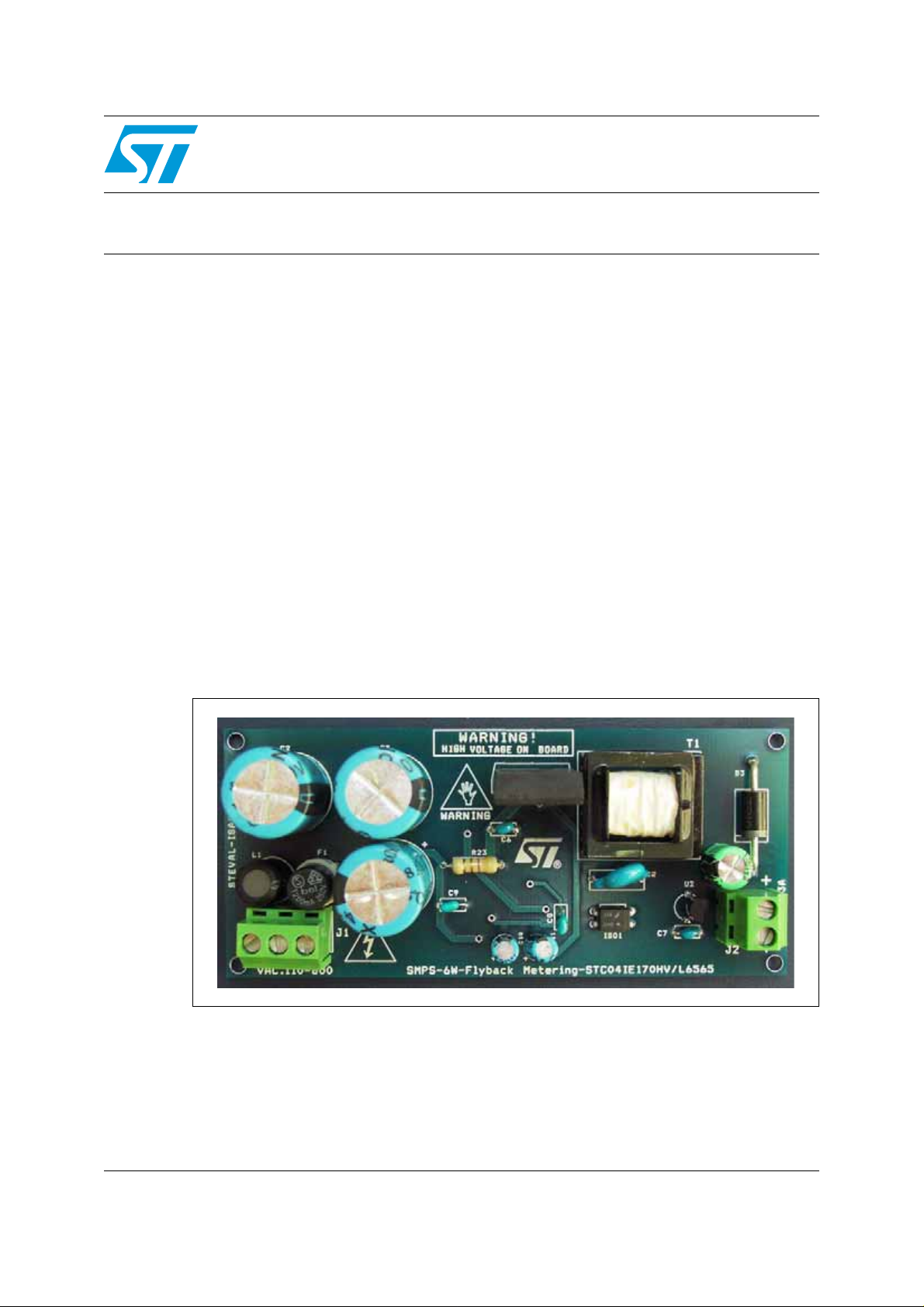
This document presents the design of a universal input power supply for metering
applications. The design is mainly based on the following ST parts: an L6565 PWM driver
and STC04IE170HP as the main switch. It is linked with the release of the STEVA LIP001Vxx demo board (see Figure 1 below). The design is a complete solution for a 5 W
single output SMPS, which is widely used as a power supply in metering applications.
However the design method can be applied to an SMPS suitable for other applications
working on a three-phase mains and it can easily be upgraded for higher ou tput power.
The ESBT base driving circuit as well as guidelines for the optimization of the power
dissipation are given.
The influence of parasitic capacitances of the transformer on the ESBT is also explained in
detail.
Finally, the most important waveforms and thermal results are given in Section 5 and
Section 6. They demonstrate the benefits of using a QR flyback with ESBT.
Refer to AN1889 and AN2254 for the overall design of an auxiliary power supply using
ESBT in flyback QR with L6565, while refer to AN2454 fo r the small signal power switch
model with all parasitic components.
Figure 1. STEVAL-ISA030V1
July 2007 Rev 1 1/21
www.st.com
Page 2

Contents AN2528
Contents
1 Design specifications and schematic diagram . . . . . . . . . . . . . . . . . . . 4
2 Flyback stage design . . . . . . . . . . . . . . . . . . . . . . . . . . . . . . . . . . . . . . . . 6
3 Parasitic capacitances and related issues . . . . . . . . . . . . . . . . . . . . . . . 8
4 Base drive circuit design . . . . . . . . . . . . . . . . . . . . . . . . . . . . . . . . . . . . . 9
5 Experimental results: waveforms . . . . . . . . . . . . . . . . . . . . . . . . . . . . . 11
6 Experimental results: efficiency and further considerations . . . . . . . 15
7 References . . . . . . . . . . . . . . . . . . . . . . . . . . . . . . . . . . . . . . . . . . . . . . . . 20
8 Revision history . . . . . . . . . . . . . . . . . . . . . . . . . . . . . . . . . . . . . . . . . . . 20
2/21
Page 3

AN2528 List of figures
List of figures
Figure 1. STEVAL-ISA030V1. . . . . . . . . . . . . . . . . . . . . . . . . . . . . . . . . . . . . . . . . . . . . . . . . . . . . . . . 1
Figure 2. Complete schematic diagram . . . . . . . . . . . . . . . . . . . . . . . . . . . . . . . . . . . . . . . . . . . . . . . . 5
Figure 3. The small signal equivalent circuit . . . . . . . . . . . . . . . . . . . . . . . . . . . . . . . . . . . . . . . . . . . . 8
Figure 4. ESBT base driving network . . . . . . . . . . . . . . . . . . . . . . . . . . . . . . . . . . . . . . . . . . . . . . . . . 9
Figure 5. DC current gain. . . . . . . . . . . . . . . . . . . . . . . . . . . . . . . . . . . . . . . . . . . . . . . . . . . . . . . . . . 10
Figure 6. Dynamic collector-source saturation voltage . . . . . . . . . . . . . . . . . . . . . . . . . . . . . . . . . . . 10
Figure 7. 110
Figure 8. 110
Figure 9. 110
Figure 10. 110
Figure 11. 380
Figure 12. 380
Figure 13. 380
Figure 14. 380
Figure 15. 600
Figure 16. 600
Figure 17. 600
Figure 18. 600
Figure 19. V
Figure 20. 110
Figure 21. 380
Figure 22. 600
Figure 23. 600
Figure 24. PCB picture top view (components and copper) . . . . . . . . . . . . . . . . . . . . . . . . . . . . . . . . 19
Figure 25. PCB picture top view components and bottom layer copper . . . . . . . . . . . . . . . . . . . . . . . 19
Figure 26. PCB picture top view components and bottom layer copper . . . . . . . . . . . . . . . . . . . . . . . 20
V
input voltage overall1 . . . . . . . . . . . . . . . . . . . . . . . . . . . . . . . . . . . . . . . . . . . . . . . 11
ac
V
input voltage overall2 . . . . . . . . . . . . . . . . . . . . . . . . . . . . . . . . . . . . . . . . . . . . . . . 11
ac
V
input voltage- storage highlight . . . . . . . . . . . . . . . . . . . . . . . . . . . . . . . . . . . . . . . 12
ac
V
input voltage turn-off highlight . . . . . . . . . . . . . . . . . . . . . . . . . . . . . . . . . . . . . . . . 12
ac
V
input voltage overall1 . . . . . . . . . . . . . . . . . . . . . . . . . . . . . . . . . . . . . . . . . . . . . . . 12
ac
V
input voltage overall2 . . . . . . . . . . . . . . . . . . . . . . . . . . . . . . . . . . . . . . . . . . . . . . . 13
ac
V
input voltage storage time highlight . . . . . . . . . . . . . . . . . . . . . . . . . . . . . . . . . . . . 13
ac
V
input voltage - turn-on highlight . . . . . . . . . . . . . . . . . . . . . . . . . . . . . . . . . . . . . . . 13
ac
V
input voltage overall1 . . . . . . . . . . . . . . . . . . . . . . . . . . . . . . . . . . . . . . . . . . . . . . . 14
ac
V
input voltage overall2 . . . . . . . . . . . . . . . . . . . . . . . . . . . . . . . . . . . . . . . . . . . . . . . 14
ac
V
input voltage turn-off highlight . . . . . . . . . . . . . . . . . . . . . . . . . . . . . . . . . . . . . . . . 14
ac
V
input voltage turn-on highlight . . . . . . . . . . . . . . . . . . . . . . . . . . . . . . . . . . . . . . . . 15
ac
vs T
comp
V
input voltage, max load . . . . . . . . . . . . . . . . . . . . . . . . . . . . . . . . . . . . . . . . . . . . . 16
ac
V
input, max load: frequency reduction. . . . . . . . . . . . . . . . . . . . . . . . . . . . . . . . . . . 17
ac
V
input, max load: further frequency reduction . . . . . . . . . . . . . . . . . . . . . . . . . . . . . 17
ac
V
input, max load: increased OFF- time highlight . . . . . . . . . . . . . . . . . . . . . . . . . . . 17
ac
(minimum OFF-time) . . . . . . . . . . . . . . . . . . . . . . . . . . . . . . . . . . . . . . . . . 16
Blank
3/21
Page 4

Design specifications and schematic diagram AN2528
1 Design specifications and schematic diagram
The table below lists the converter specification data and the main parameters fixed for the
demo board.
Table 1. Converter specification and p r eliminary choices
Symbol Description Values
V
inmin
V
in
V
out
P
out
η Converter efficiency @ max load > 80%
F Minimum switching frequency ≅
V
fl
V
spike
Rectified minimum input voltage 150
Rectified maximum input voltage 850
Output voltage 14 V/430 mA
Maximum output power 6 W
30 kHz
Reflected flyback voltage 250 V
Max over voltage limited by clamping circuit 150 V
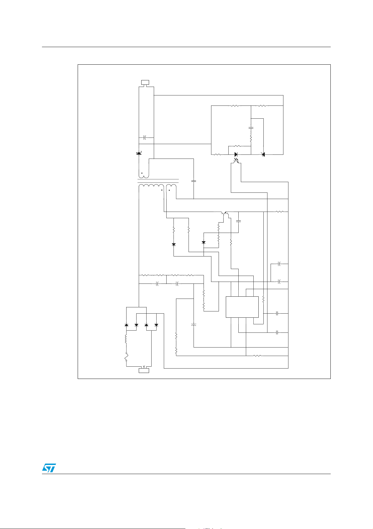
A schematic diagram of the SMPS is given in Figure 2. The most relevant components are:
1. HV ESBT main switch and simple driving circuit
2. L6565 QR PWM driver to get the best efficiency
3. Special transformer construction with very low parasitic capacitance
4/21
Page 5
AN2528 Design specifications and schematic diagram
Figure 2. Complete schematic diagram
J2
Phoenix 2 pin12
R14
14V @ 0.43A
C1
330uF/25V
+
D7
C5
.0022uF
AC
Y1 cap
13
LL4148
R11
ISO1
H11A817
Q1
R12
R24
D3
STPS3L60U
A C
35T
7
6
7
6
T1
1
CSM 2010-104
1
48T
2
2
334
27T
R6
1/ 1/8W
D6
LL4148
9T
4
R8
47k/ 1/ 8W
AC
11K/ 1/ 8W
R21
2.4K/ 1/8W
10nF
C7
R17
R15
1.2K/ 1/8W
1.5K/ 1/8W
12
43
STC04IE170HP
4
2
C6
10/ 1206
R13
2.2K/ 1206
22/ 1206
10nF
4.7K/ 1/8W
U2
TL431_ARC
R
A C
R23
4.7/ 1/4W
C11
22uF/25V
+
R2
R1
AC
STTH112U
STTH112U
D1
D2
D4 STTH112U
A C
M600X
L1
F1
TR5FU S E
1 2
J1
100K/ 1206
100K /1206
+
C2
33uF/450V
AC
D5
STTH112U
A C
123
Phoenix 3 pin
R7
R3
100K/ 1206
100K/ 1206
+
C3
33uF/450V
R5
1M
R4
1M
100K/1206
R10
R9
100K/ 1206
+
C4
33uF/450V
8
6
7
5
GD
Vcc
U1
INV
L6565
1
ZCD
GND
Vff
COMP
CS
3
2
4
R18
22K
C10
47uF/25V
+
R22 330
4.7nF
C9
3.3nF
C8
5/21
Page 6

Flyback stage design AN2528
2 Flyback stage design
Well known to all SMPS designers, the voltage stress on the device (power switch) is given
by:
Equation 1
V
V
off
inmaxVflVspike
where V
= flyback voltage = (V
fl
out
+ V
F, diode
collector due caused by leakage inductance. This over-voltage is not limited by any
clamping network in order to minimize as much as possible the solution cost using also the
very large margin available which has been fixed to 200 V. N
primary side while Ns is the number of turns on the main output secondary winding.
Now, taking into account a 300 V margin, the maximum flyback voltage that can be chosen
is:
Equation 2
V
BV V
fl
– V
inmax
– V
spike
minarg
After the calculation of the flyback voltage, we can proceed with the next step in the
converter design. The turns ratio between primary and secondary side is calculated with the
following formula:
––=
) * Np/Ns and V
1700 850– 200– 300 350V=–=–=
is the over-voltage on the
spike
is the number of turns on the
p
Equation 3
N
------ -
N
p
s
V
+
outVF diode,
fl
---------------------------------------- -
V
350
--------------- -
14 1+
23.3===
As a first approximation, since t he turn-on of the device occurs immediately after the energy
stored on the primary side, inductance is completely transferred to the secondary side:
Equation 4
V
• VflT
dcminTonmax
•=
reset
and
Equation 5
Where T
is the maximum on time, T
onmax
transformer inductance and T
T
results in:
onmax
T
is the switching time. Combining the two previous formulas
S
– TS=
onmaxTreset
is the time needed to demagnetize the
reset
Equation 6
VflT
•
T
onmax
------------------------------ -
V
S
+
dcminVfl
14µs≅=
The next step is to calculate the peak current. The output power is set to 6 W and the
desired transformer efficiency must be set by the designer (at least 80% in this case).
Excluding the energy losses on the input diode bridge, on the power switch and on the
secondary side rectifier, the following approximate formula can be used:
6/21
Page 7

AN2528 Flyback stage design
N
Equation 7
1
-- -
LPI
P
1.25 P
IN
•
OUT
2
------------------------------=
T
s
1
2
••
P
2
-- -
V
• T
dcmin
2
---------------------------------------------------------- -==
L
PTS
2
•
onmax
•
Hence
Equation 8
2
V
dcmin
------------------------------------------------ -
L
P
2.5 T
T
•
• P
•
S
2
onmax
OUT
14.7mH==
From here we can now calculate the peak current on primary.
Equation 9
V
•
dcminTonmax
-------------------------------------------
I
P
L
P
143mA≈=
To keep the transformer size v ery small and to get a very effe ctiv e cost solution , we pref er to
slightly increase the minimum working frequency in order to decrease the primary
inductance.
In order to hav e a 15 mH indu ctance and to k e ep an EF20 co re, a lo t of turns are needed on
the primary side. This can generate either not enough space on the EF20 core to
accomodate such a high number of windings or the remaining space is not large enough to
ensure good design. These considerations might induce designing a smaller primary
inductance value accepting a higher switching frequency.
There is no contraindication in using a smaller primary inductance which leads to a higher
minimum switching frequency and theoretically also to a higher maximum frequency.
Howev er the maxim um switching frequency is then limited not only by the inductance value,
but also by the L6565 PWM driver. When using an L6565, the internal blanking time limits
the minimum off-time and, in turn, the maximum switching frequency. To better understand
this phenomenon, please refer to the L6565 datasheet and to the next paragraphs.
After bench tests and fine tuning we used a transformer with the following specs:
Equation 10
L
7.5mH=
P
Equation 11
------ -
N
p
23.8=
s
N
------------
N
aux
p
18.87=
The part number of the transformer is CSM 2010-104 from Cramer.
In the next Section 3, we see from bench verification that the real minimum working
frequency is 50 kHz even if the inductance is 7.5 mH but with a peak current of about
250 mA.
7/21
Page 8

Parasitic capacitances and related issues AN2528
3 Parasitic capacitances and related issues
In a flyback converter stage it is important to take into account the parasitic capacitances
since their influence may affect the correct operation of the converter itself. Figure 2 shows
the small signal equivalent model of a main switch, transformer and main parasitic effects.
The parasitic capacitances between the ESBT collector and ground are mainly due to three
components (see Figure 2):
1. C
2. C
3. C
Usually transistors are mounted on a heat-sink by interposing an insulation layer. The heat-
sink has to be grounded either for safety reasons, or to minimize the RFI. The resulting total
parasitic capacitance C is equal to C
additional and non-negligible s witch-on po wer dissip ation. Large para sitic capacitances ma y
cause ringing and produce noise problems. The effect of parasitic capacitances is worse at
higher input voltages, like those observed in a 3-phase power supply.
Figure 3. The small signal equiv alent circuit
, the primary inter-winding capacitance;
1
, the intrinsic capacitance of ESBT between its collector and source;
2
, the parasitic capacitance between the collector of the ESBT and the heat-sink.
3
+ C2 +C3. C may be large enough to produce
1
+
Cbus
ESBT
T
I nsula ion Pad
Heatsink
C1
ESBT
C3
C2
T
C1
Ic1
Heatsink
ESBT
C2
Ic
T
Ic2
C3
Ic3
Considering that the power managed by the system is low, another goal to achieve is to
keep the power dissipation very low on every part on the system. Our target is to get less
than 1.5 W power loss on the switch. Achieving this target leads to two benefits: high
efficiency and no need of heat-sink (cost reduction).
Therefore the effect of C
additional power dissipation during switch-on and does not affect system stability. C
must not be considered in this case. C2 is related only to
3
has
1
the most important effect on flybac k con verter design. We hav e only tw o w a ys t o reduce C
1. Parasitic transformer inter-winding capacitance
2. Layout parasitic capacitance
Care is needed when designing the layout and building the transformer.
:
1
8/21
Page 9

AN2528 Base drive circuit design
4 Base drive circuit design
Let's have a closer look at the very simple base drive network used in this application.
Normally in applications such SMPS, where the load is variable, the collector current varies
as well. It is very important to provide a base current to the device that is correla ted with the
collector current in order to avoid the over saturation of the de vice at low load and to
optimize its performance in terms of power dissipation. This implies the use of a driving
network which allows getting a base current proportional to the collector current. For
additional information about the ESBT proportional base driving method, refer to AN2131.
Since in our application we must take into account power dissipation and simplicity as well,
we have pr eferred the simplest and least expensive driving network which is shown in
Figure 4. This choice also satisfies power dissipation requirements.
To set the R
value some considerations must be done. First of all, ref er to the hFE curve of
CC
STC04IE170HP (Figure 5).
Figure 4. ESBT base driving network
Referring to the calculations in Section 2, the collector peak current is 250 mA. At this
current value the ESBT gain is about 20, so that theoretically just 250 / 20 = 12.5 mA should
be enough to drive the base. This is true for very long conduction time. In the present
example the dynamic phenome non can occur du e t o th e re lati vely high switching fr eq ue ncy
(higher than 50 kHz) and even more to the small conduction time.
This concept is illustrated in Figure 6. It is extracted from the STC04IE170HP datasheet and
shows that, right after the turn-on, the V
needs some time to reach the V
CS
CSSAT
value. This
time is proportional to the collector current amount. That is why a peak base current is
absolutely mandatory to have a low voltage drop during conduction as soon as possible.
For further details about the driving network, please refer to AN2454.
9/21
Page 10

Base drive circuit design AN2528
Figure 5. DC current gain
Figure 6. Dynamic collector-source saturation voltage
To maximize performances, a base capacitor C
Note that, using the driving network shown in Figure 4, a quasi total recovery of energy to
drive the base is achieved. During the storage time the collector current comes out from the
base and is stored in the base capacitor. If the capacitor is small enough, the voltage across
it reaches the V
and after that the current flows to the Vcc capacitor.
cc
To set the time duration of the base current spike, the following appr oximate formula is
useful:
Equation 12
t
peak
Since R
=10 Ω (see below), if the peak has to be about 300 ns
B
Equation 13
C
B
The aim of R
is to dampen the ringing on the base current at the end of its peak. It is
B
chosen as a compromise between a dampi ng effect and additional power dissipation on it.
10/21
3R
• CB•=
t
peak
---------------- -
3R
•
B
has been inserted.
B
B
10nF==
Page 11

AN2528 Experimental results: waveforms
Ten is big enough to remove any ringing and the additional power dissipation on it is
practically negligible due to the very low current flowing through it. Finally, knowing that V
cc
is about 15 V:
Equation 14
15V
CC
-------------------- -
12.5mA
1.2KΩ==
R
After bench verification a final R
forecasted one flows into the base (higher I
during the peak (much lower I
of 2.2 kΩ has been fixed. A smaller base current than the
CC
ratio for a very short time).
C/IB
ratio) compensated by a higher base current
C/IB
5 Experimental results: waveforms
The following f igures sho w t he main w a veforms in steady state condition at full load. Notice
the behavior of the base current with an initial high peak pulse needed t o minimize th e eff ect
of the dynamic saturation voltage.
Figure 7. 110 V
input voltage overall1
ac
Figure 8. 110 V
input voltage overall2
ac
11/21
Page 12

Experimental results: waveforms AN2528
Figure 9. 110 Vac input voltage- storage highlight
Figure 10. 110 V
Figure 11. 380 V
input voltage turn-off highlight
ac
input voltage overall1
ac
12/21
Page 13

AN2528 Experimental results: waveforms
Figure 12. 380 Vac input voltage overall2
Figure 13. 380 V
Figure 14. 380 V
input voltage storage time highlight
ac
input voltage - turn-on highlight
ac
13/21
Page 14

Experimental results: waveforms AN2528
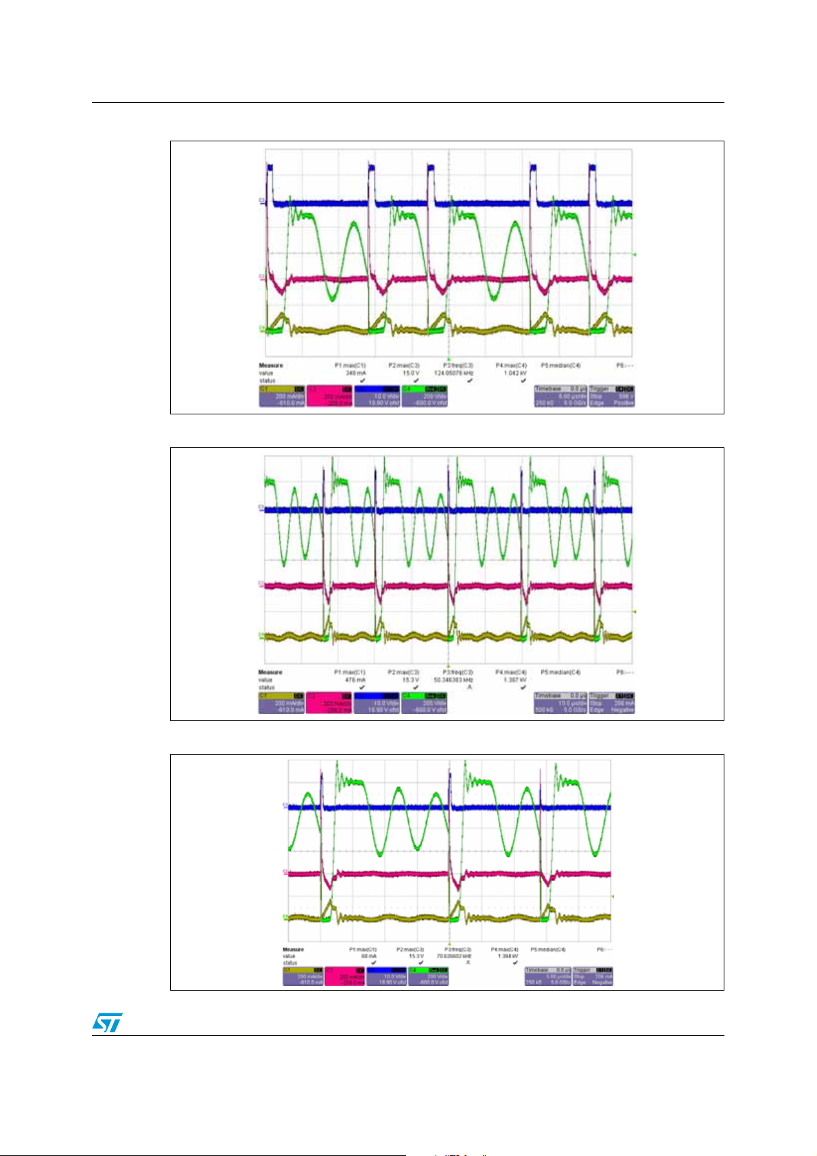
Figure 15. 600 Vac input voltage overall1
Figure 16. 600 V
Figure 17. 600 V
input voltage overall2
ac
input voltage turn-off highlight
ac
14/21
Page 15

AN2528 Experimental results: efficiency and further considerations
Figure 18. 600 Vac input voltage turn-on highlight
The importance of having a very good transformer in the turn-on highlight at high input
voltage can be better observed. The collector cur rent leading edge at turn-on is evident in
this condition. The peak amplitude has to be controlled or it can lead to premature turn-off of
the PWM driver with consequent instability. This issue has been deeply discussed in
Section 3.
6 Experimental results: efficiency and further
considerations
Table 2 summarizes the thermal and loss data. All information refers to max load. An
excellent result is the very high efficiency also at the highest input voltage. The case
temperature of ESBT is fine even in the worst case, with consequent low power dissipation
on it.
Table 2. Power dissipation and efficiency
VinAC (V) Tc (°C) Ptot (W) Efficiency
110 (V) 34 0.3 80%
400 (V) 49 0.8 66%
600 (V) 73 1.6 55%
To get the thermal performances shown, a special feature of the bi polar ha s been positively
utilized.
In a standard QR mode of operation, when the input voltage rises higher and higher, the
switching losses should increase since the frequency is increasing. For this reason the
L6565 provides the frequency foldback function that limits the minimum OFF-time.
An added feature is given by the storage time of ESBT, that helps to further reduce the
frequency while increasing the Input Voltage and/or reducing the load. This frequency
15/21
Page 16
Experimental results: efficiency and furt her considerations AN2528
reduction at high input voltage is very effective in improving the overall efficiency, since the
higher turn-on and turn-off voltages make the switching losses critical.
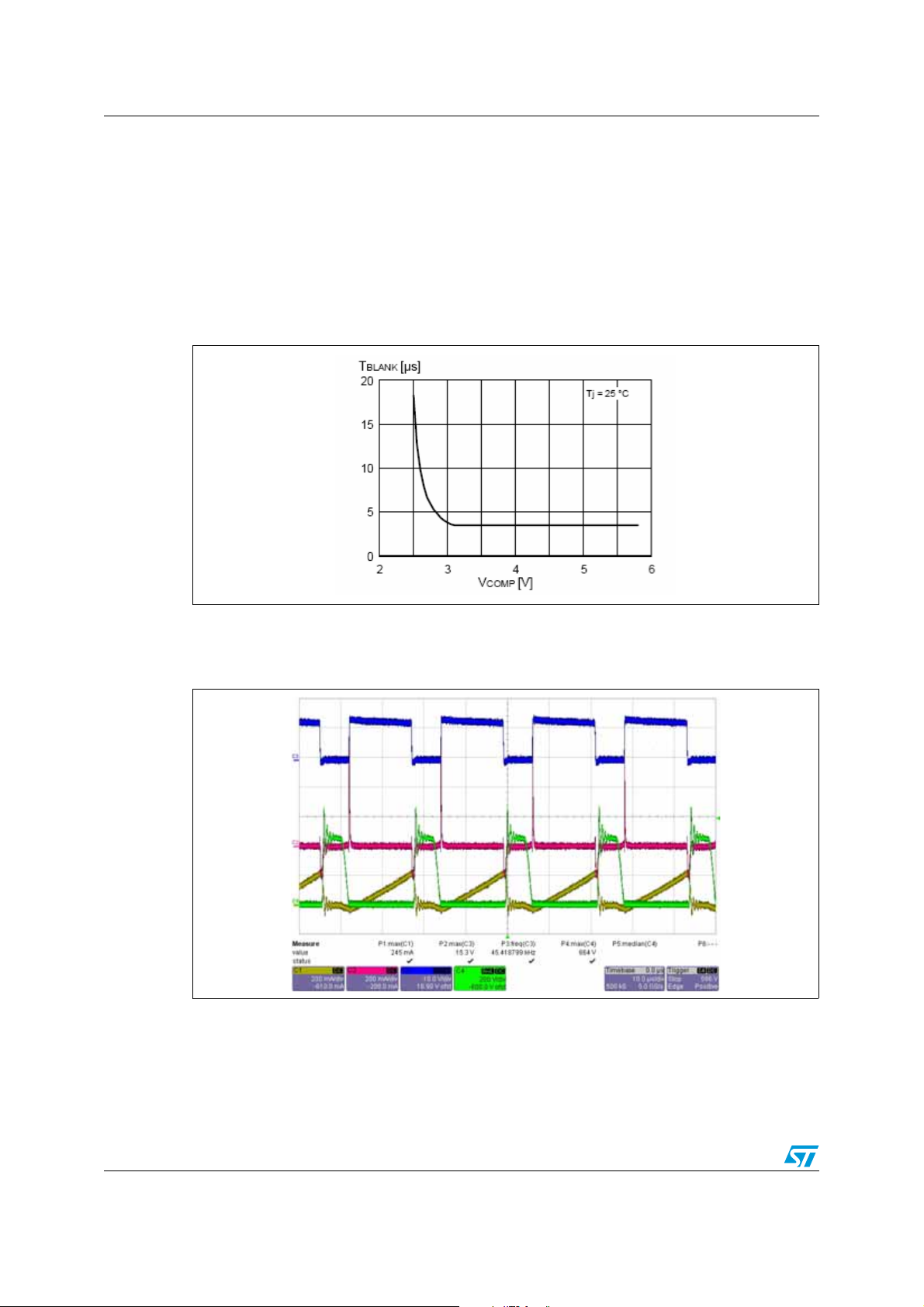
Thanks to the storage time (lasting about 1.5 µs under this condition), that adds a delay to
the current on-time, the minimum on-time is much longer than the one impo se d by the
L6565.
This leads to a lower V
value, and as a consequence, to a longer minimum OFF-time
comp
(see Figure 19 below). The system then works in advance at lower frequency as soon as
the input voltage increases or the load decreases.
Figure 19. V
comp
vs T
(minimum OFF-time)
Blank
In the next figures the frequency reduction as a consequence of an increased input voltage
is shown.
Figure 20. 110 V
input voltage, max load
ac
From Figure 21 the frequency is reduced due to the storage time presence at 380 V
becoming more and more evident at higher input voltage, 600 V
This "enhanced" frequency foldback created by the storage time allows keeping the total
power dissipation on the device very low regardless of the very high voltage needed to
sustain.
16/21
ac
,
ac
.
Page 17
AN2528 Experimental results: efficiency and further considerations
Figure 21. 380 Vac input, max load: frequency reduction
Figure 22. 600 V
Figure 23. 600 V
input, max load: further frequency reduction
ac
input, max load: increased OFF- time highlight
ac
17/21
Page 18

Bill of materials AN2528
Appendix A Bill of materials
Table 3. Bill of materials
Reference Qty Value/part number Description
C1 1 330 µF / 25V Electrolytic capacitor
C2, C3, C4 3 33 µF / 450V Electrolytic capacitor
C5 1 .0022 µF ceramic capacitor, 440 V
C6, C7 2 10 nF / 50 V ceramic capacitor, 50 V, X7R
C8 1 3.3 nF / 50 V ceramic capacitor, 50 V, X7R
C9 1 4.7 nF / 50 V ceramic capacitor, 50 V, X7R
C10 1 47 µF / 25 V Electrolytic capacitor
C11 1 22 µF / 25 V Electrolytic capacitor
D1, D2, D4, D5 4 STTH112U STMicroelectronics, diode rectifier, 1200 V, 1 A
D3 1 STPS3L60 STMicroelectronics, diode power schottky, 60 V, 3 A
D6, D7 2 LL4148 SMD 1206
F1 1 TR5Fuse Serie TR5 250 mA / 250 V
ISO1 1 H11A817 Phototransistor Optocouplers, Fairchild
J1 1 Phoenix 3 pin
J2 1 Phoenix 2 pin
L1 1 M600X Radiali, 470 µH
Q1 1 STC04IE170HP
R1, R2, R3, R7, R9, R10 6 100 K SMD 1206
R4, R5 2 1 M SMD 1206
R6 1 1 SMD 1206
R8 1 47 K SMD 1206
STMicroelectronics, emitter switched Bipolar transistor,
4 A, 1700 V
, 2 KV
ac
R11 1 1.5 K SMD 1206
R12 1 10 SMD 1206
R13 1 22 SMD 1206
R14 1 11 K SMD 1206
R15 1 1.2 K SMD 1206
R17 1 4.7 K SMD 1206
R18 1 22 K SMD 1206
R21 1 2.4 K SMD 1206
R22 1 330 SMD 1206
R23 1 4.7 / 1/2 W Resistor, carbon film, 350 V, 0.5 W, 5%
18/21
Page 19

AN2528 PCB layout
Table 3. Bill of materials (continued)
Reference Qty Value/part number Description
T1 1 CSM 2010-104 CRAMER [sample]
U1 1 L6565 STMicroelectronics, Q-resonant SMPS controller
U2 1 TL431C STMicroelectronics, Shunt Reference, 2,5 V, 1 to 100 mA
Appendix B PCB layout
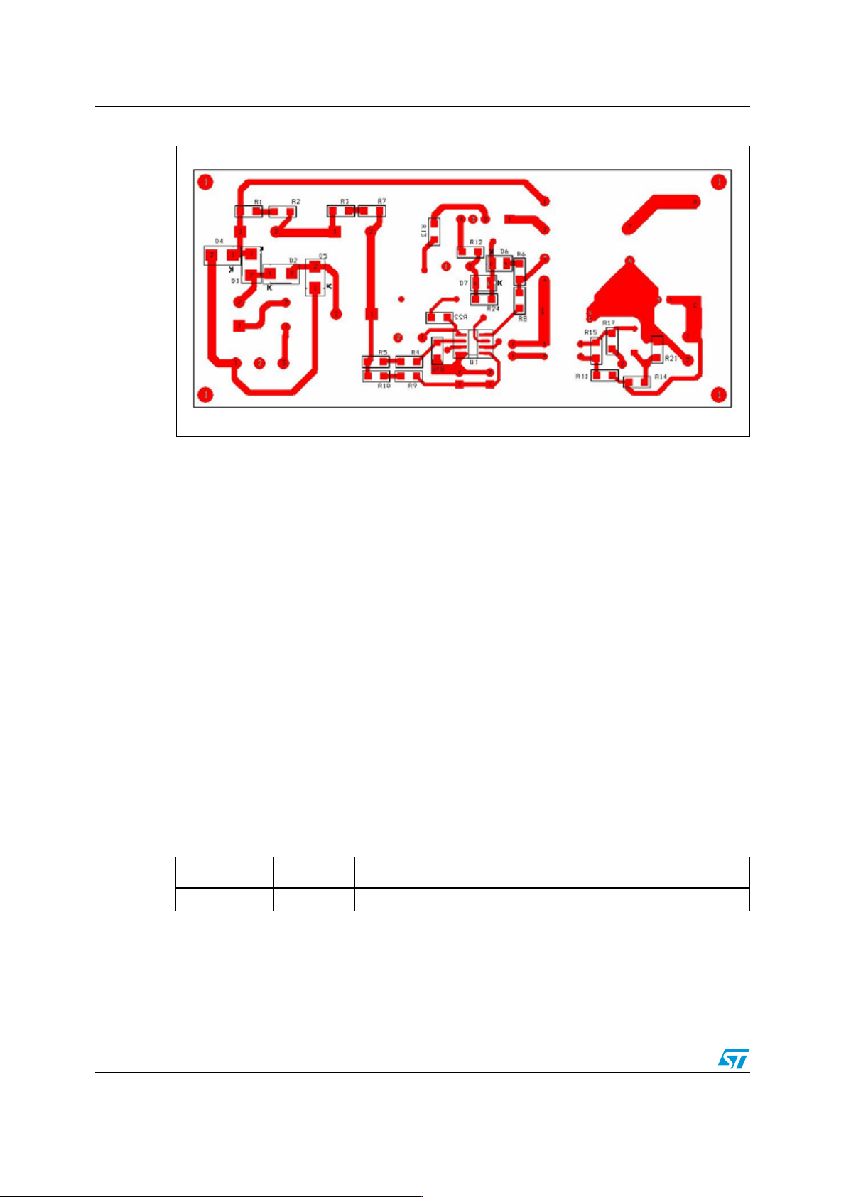
Figure 24. PCB picture top view (components and copper)
Figure 25. PCB picture top view components and bottom layer copper
19/21
Page 20
References AN2528
Figure 26. PCB picture top view components and bottom layer copper
7 References
● STMicroelectronics application note AN1889 "ESBT STC03DE120 IN 3-PHASE
AUXILIARY POWER SUPPLY”
● STMicroelectronics application note AN1262 "OFFLINE FLYBACK CONVERTERS
DESIGN METHODOLOGY WITH THE L6590 FAMILY"
● STMicroelectronics application note AN2131 "HIGH POWER 3-PHASE AUXILIARY
POWER SUPPLY DESIGN BASED ON L5991 AND ESBT STC08DE150"
● STMicroelectronics L6565 datasheet
● STMicroelectronics STC04IE170HV datasheet
● "Switching Power Supply Design", McGraw-Hill, Inc.
8 Revision history
Table 4. Revision history
Date Revision Changes
05-Jul-2007 1 First issue
20/21
Page 21

AN2528
Please Read Carefully:
Information in this document is provided solely in connection with ST products. STMicroelectronics NV and its subsidiaries (“ST”) reserve the
right to make changes, corrections, modifications or improvements, to this document, and the products and services described herein at any
time, without notice.
All ST products are sold pursuant to ST’s terms and conditions of sale.
Purchasers are solely res ponsibl e fo r the c hoic e, se lecti on an d use o f the S T prod ucts and s ervi ces d escr ibed he rein , and ST as sumes no
liability whatsoever relati ng to the choice, selection or use of the ST products and services described herein.
No license, express or implied, by estoppel or otherwise, to any intellectual property rights is granted under this document. If any part of this
document refers to any third pa rty p ro duc ts or se rv ices it sh all n ot be deem ed a lice ns e gr ant by ST fo r t he use of su ch thi r d party products
or services, or any intellectua l property c ontained the rein or consi dered as a warr anty coverin g the use in any manner whats oever of suc h
third party products or servi ces or any intellectual propert y contained therein.
UNLESS OTHERWISE SET FORTH IN ST’S TERMS AND CONDITIONS OF SALE ST DISCLAIMS ANY EXPRESS OR IMPLIED
WARRANTY WITH RESPECT TO THE USE AND/OR SALE OF ST PRODUCTS INCLUDING WITHOUT LIMITATION IMPLIED
WARRANTIES OF MERCHANTABILITY, FITNESS FOR A PARTICUL AR PURPOS E (AND THEIR EQUIVALE NTS UNDER THE LAWS
OF ANY JURISDICTION), OR INFRINGEMENT OF ANY PATENT, COPYRIGHT OR OTHER INTELLECTUAL PROPERTY RIGHT.
UNLESS EXPRESSLY APPROVED IN WRITING BY AN AUTHORIZED ST REPRESENTATIVE, ST PRODUCTS ARE NOT
RECOMMENDED, AUTHORIZED OR WARRANTED FOR USE IN MILITARY, AIR CRAFT, SPACE, LIFE SAVING, OR LIFE SUSTAINING
APPLICATIONS, NOR IN PRODUCTS OR SYSTEMS WHERE FAILURE OR MALFUNCTION MAY RESULT IN PERSONAL INJ URY,
DEATH, OR SEVERE PROPERTY OR ENVIRONMENTAL DAMAGE. ST PRODUCTS WHICH ARE NOT SPECIFIED AS "AUTOMOTIVE
GRADE" MAY ONLY BE USED IN AUTOMOTIVE APPLICATIONS AT USER’S OWN RISK.
Resale of ST products with provisions different from the statements and/or technical features set forth in this document shall immediately void
any warranty granted by ST fo r the ST pro duct or serv ice describe d herein and shall not cr eate or exten d in any manne r whatsoever , any
liability of ST.
ST and the ST logo are trademarks or registered trademarks of ST in vari ous countries.
Information in this document su persedes and replaces all information previously supplied.
The ST logo is a registered trademark of STMicroelectronics. All other names are the property of their respective owners.
© 2007 STMicroelectronics - All rights reserved
STMicroelectronics group of compan ie s
Australia - Belgium - Brazil - Canada - China - Czech Republic - Finland - Fran ce - Germany - Hong Kong - India - Israel - Italy - Japan -
Malaysia - Malta - Morocco - Singapore - Spain - Sweden - Switzerland - United Kingdom - United States of America
www.st.com
21/21
 Loading...