

Page 1
AN2526
r
Application note
STMAV340 evaluation board & PCB layout recommendation
Introduction
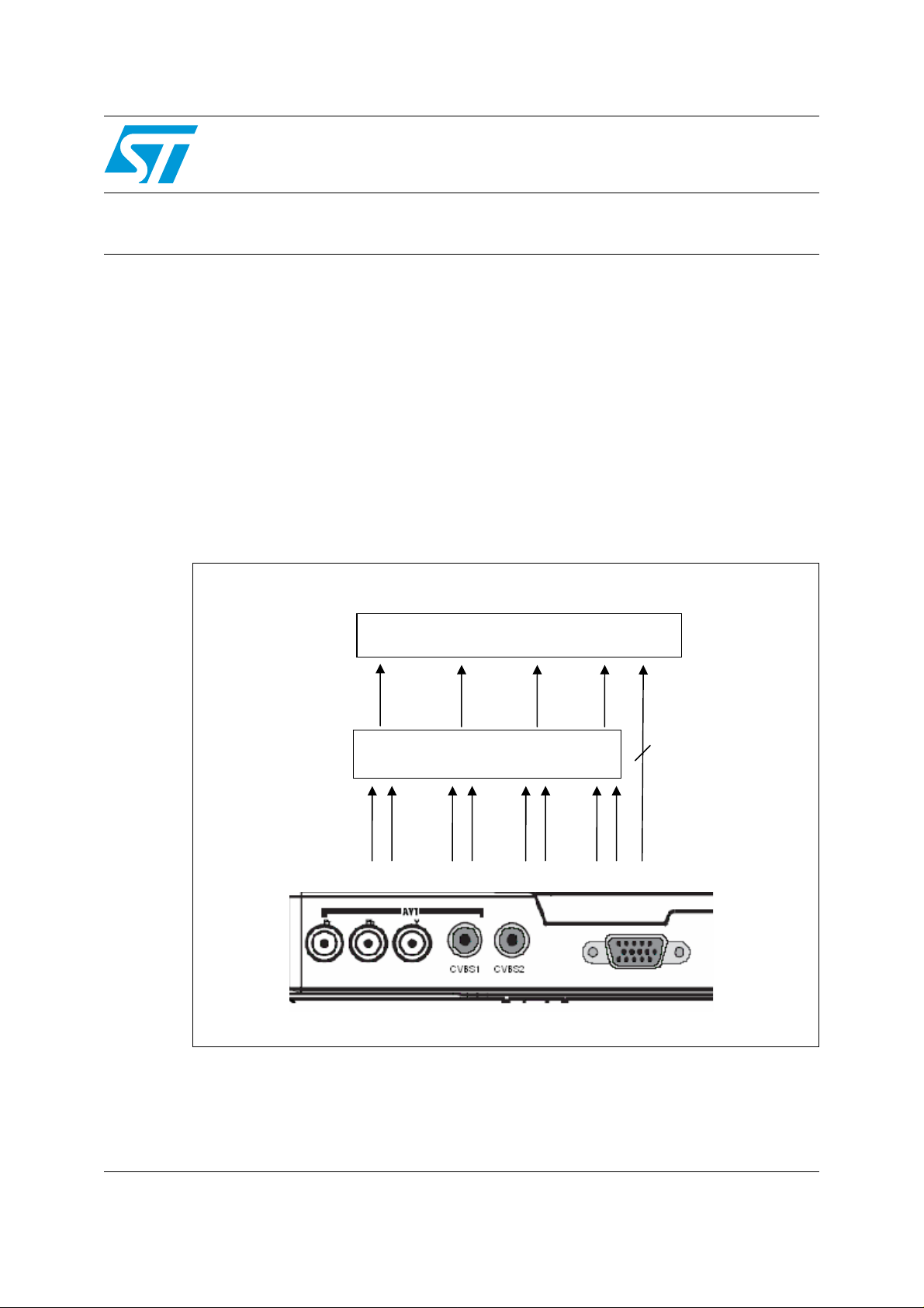
STMA V34 0 has 4 chan nels an d a 2 to 1 video switch that is well suited for switching analog
video signals on a TV or monitor set. Below is a diagram of STMAV340 typical application
configuration. As illustrated on the picture below , the 3 channels of the s witch can be used to
switch two complete sets of RGB a nd YPbPr to a single RGB/YPbPr output. One additio nal
channel can be used to switch 2 CBVS inputs to a single output that can be directly
connected to a single CVBS receiver input.
Without STMAV340 integrated in the system, the video receiver needs to have more input
pins to accommodate the many video inputs at the back panel. With the introduction of
STMAV340, less IO pins are required at the video receiver. Together with the optimized pin
arrangement, the result is a straightforward system design and overall cost reducti on.
STMAV340 in a TV application
VIDEO RECEIVER
G/Pb B/P
CVBS
STMAV340
R Y G Pb B Pr CVBS1/2
H/V SYNC
ID/VESA
April 2007 Rev 1 1/10
www.st.com
Page 2

Contents AN2526
Contents
1 Evaluation board . . . . . . . . . . . . . . . . . . . . . . . . . . . . . . . . . . . . . . . . . . . . 3
2 PCB layout recommendation . . . . . . . . . . . . . . . . . . . . . . . . . . . . . . . . . . 6
3 Revision history . . . . . . . . . . . . . . . . . . . . . . . . . . . . . . . . . . . . . . . . . . . . 9
2/10
Page 3

AN2526 Evaluation board
1 Evaluation board
The evaluation board was designed with trouble-free customer evaluation in mind. Instead
of having two sets of RGB (VGA connector) and YPbPr (RCA connector) as inputs and
branching the output to the VGA and RCA connectors, two VGA RGB inputs are connected
and the outputs go directly to single VGA connector t o a display unit.
For the evaluation, the customer can connect the two sets of inputs to two VGA port of PC,
while the output can be directly connected to the VGA port of the display unit.
● Power supply
The board can be powered e ither directly f rom a DC po wer su pply or from a DC adaptor. If it
is powered from DC power supply, 5VDC is connected to the power socket labeled V
and the ground is connected to the power socket labeled GND. The board can also be
powered from a DC adaptor having output voltage of 7 V to 15 V. The DC adaptor voltage is
regulated to 5 V by the on board regulator. The DC adaptor can be center positive or
negative and it should be connected to the DC JACK.
To prevent the digital lines s witching from coup ling to the analog lines , the pow er distribution
is separated from digital and analog sections. Although STMAV340 has also two digital
lines, which are OE and SEL, it should still be powered from the analog supply because its
main function is to switch analog signals and those two digital lines are mostly static during
operation. Hence the analog lines are not disturbed b y t he digital pa rt and, as such, there is
no need to have a separate analog and digital supply for STMAV340.
CC
5V
The analog and digital sections on the board are isolated by ferrite beads.
Table 1. STMAV340 Demo board power supply
Designator Notes
V
5V Connect to 5 V of external power supply.
CC
GND Connect to ground of external power supply.
DC JACK
Connect to DC adaptor output if the board is to be powered from DC
Note: External power can be applied to either V
● Video input & output ports
There are four video input ports: VGA1, V GA2, CVBS1, and CVBS2. STMAV340 performs
the switching of these video inputs. Depending on the SEL control line, either VGA1 or
VGA2 input is directed to VGA_OUT and either CVBS1 or CVBS2 is directed to
CVBS_OUT.
Since STMAV340 does not perform the switching of VGA syn ch ro niz at ion sign als, two
STG719 are incorporated to switch both horizontal and vertical synchronization.
VGA port also has some ID signals. To pre vent clashing between ID signals from VGA input
1 and 2, the ID lines are isolated by jumpers. If VGA1 is active and to be directed to
VGA_OUT, JP1 to JP4 should be closed whereas JP5 to JP8 should be ope ned. If VGA2 is
active and to be directed to VGA_OUT, JP5 to JP8 should be closed whereas JP1 to JP4
should be opened.
adaptor. Input voltage: 7 to 15 V
5V/GND or DC JACK, but not to both.
CC
3/10
Page 4
Evaluation board AN2526
Table 2. Video ports on the STMAV340 Demo board
Designator Notes
– Connect to VGA source from PC.
VGA1
VGA2
– When SEL ‘0’ this port is active
– JP1 to JP4 closed.
– JP5 to JP8 open.
– Connect to VGA source from PC
– When SEL ‘1’ this port is active
– JP1 to JP4 open.
– JP5 to JP8 closed.
CVBS1
CVBS2
VGA_OUT Active VGA input is directed to this port. Connect to a display unit.
CVBS_OUT Active CVBS input is directed to this port. Connect to a display unit.
● Video inputs conditioning
– Connect to CVBS source
– When SEL ‘0’ this port is active
– Connect to CVBS source
– When SEL ‘1’ this port is active
The blanking level might vary between different video transmitters. This STMAV340
evaluation board can handle video signals with blanking level of 0 V to 2.5 V.
If video signals blanking lev el at ou tside the abov e r ange, so me input conditioning should be
done to translate the blanking level to the range specified.
● Digital control signals
Table 3. Control signals on the STMAV340 Demo board
Signal Function Notes
OE
SEL
Enable or disable the
output.
Select which switch is
activated.
JP9 close = LOW (enable)
JP9 open = HIGH (disable)
JP10 close = LOW (VGA1, CVBA1)
JP10 open = HIGH
(VGA2, CVBS2)
4/10
Page 5

AN2526 Evaluation board
Figure 1. STMAV340 Evaluation board schematic
Table 4. Bill of materials (BOM)
No Component Designator Package Manufacturer
1 STMAV340 U1 TSSOP16 STMicroelectronics
2 STG719STR U2, U3 SOT23-6L STMicroelectronics
3 VGA FEMALE CON VGA1, VGA2, VGA_OUT
4 RCA CON CVBS1, CVBS2, CVBS_OUT
5 LD1117V50 U5 TO-220 STMicroelectronics
6 DF04M RECTIFIER U4 DFM GENERAL SEMI
7 DC JACK DC JACK
8 POWER SOCKET V
9 FERRITE BEAD L1, L2 1206
10 100 nF Cap C2,C3, C5 0603
11 10 µF Electrolytic Cap C1, C4 Cap7.62 mm
5V, GND
CC
5/10
Page 6

PCB layout recommendation AN2526
Table 4. Bill of materials (BOM) (continued)
No Component Designator Package Manufacturer
12 Jumper
13 10k Resistor R1, R2 0603
JP1, JP2, JP3, JP4, JP5, JP6,
JP7, JP8, JP9, JP10.
2 PCB layout recommendation
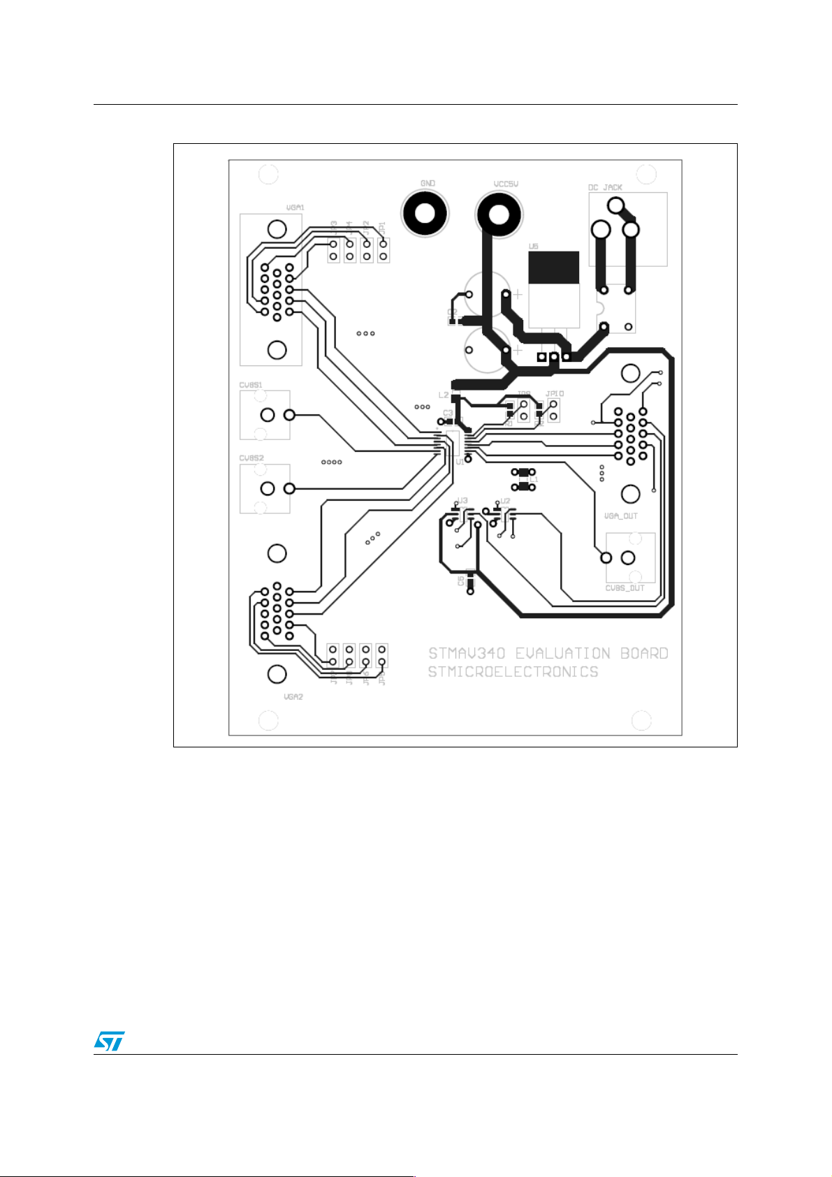
For the purpose of maintaining 75 Ω track for all the analog lines, a 4-layer structure is
recommended. All the analog tracks are rout ed on the top lay er of the board. The middle t wo
layers are used for both analog and digita l ground.
The middle two layers are identical and separated into two sections, analog and digital
grounds. They are separ a ted by a slot area and are only connected at the top layer through
ferrite bead. This ensures that the digital switching noise does not get coupled to the analog
portion.
All the analog tracks are routed on top of the analog ground and all the digital tracks are
routed on top of digital ground. There is one signal, the SEL line, which needs to cross from
analog to the digital portion. The crossing is done at the bottom layer exactly below where
the ferrite bead is used to bridge the analog and digital ground. Since the SEL digital line is
mostly static during operation, it does not cause any disruption to the analog portion.
STMAV340 supply is connected to V
the stability of STMAV340 supply, a 100 nF capacitor is used to decouple the V
stability of the analog supply lines is of significant importance since the bias level of
STMAV340 is referenced to it. Any instability on the analog supply affects the switch
characteristics.
5V analog and GND analog. To further guarantee
CC
HDR 2X1
pin. The
CC
Each set of video signals, RGB1, RGB2, and RGB_OUT are routed with the same track
length. This guarantees minimum channel-to-channel delay. To guarantee the impedance
match on the analog lines, no via is used for routing these signals.
6/10
Page 7
AN2526 PCB layout recommendation
Figure 2. PCB Top layer
7/10
Page 8

PCB layout recommendation AN2526
Figure 3. PCB Middle layer
8/10
Page 9
AN2526 Revision history
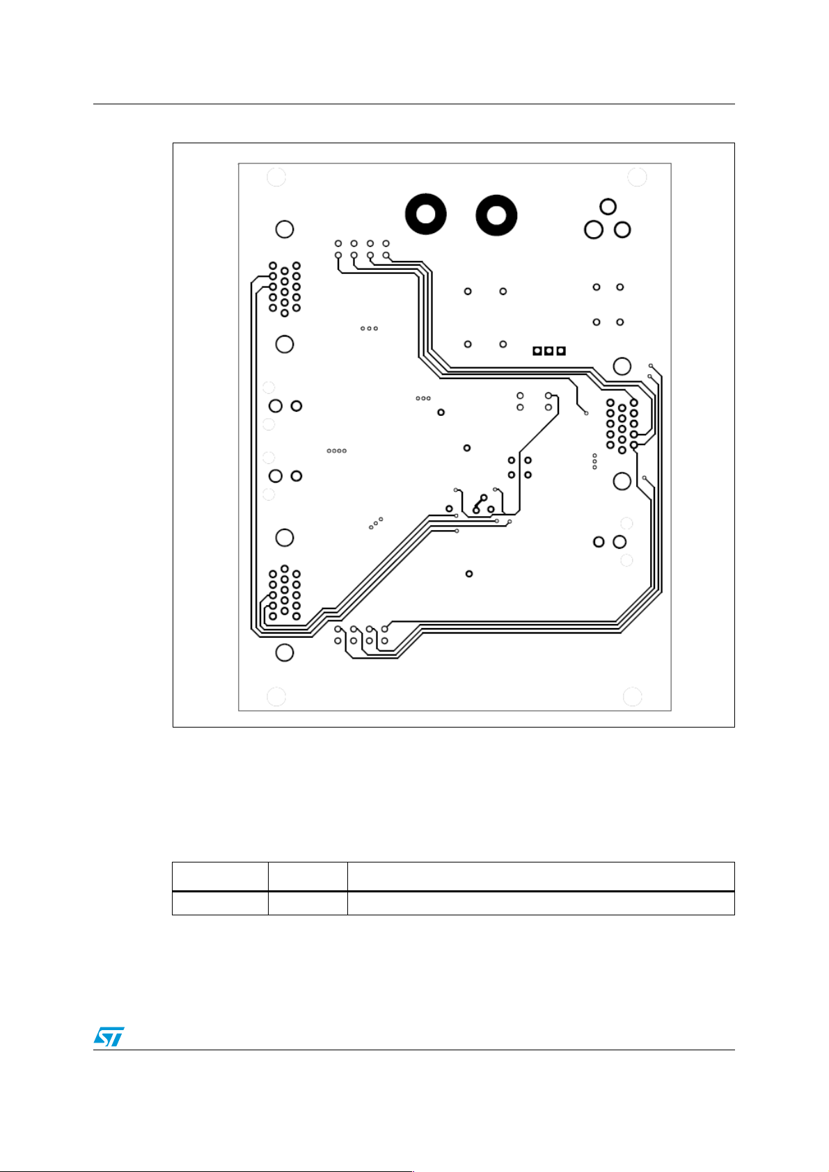
Figure 4. PCB Bottom layer
3 Revision history
Table 5. Revision history
Date Revision Changes
30-Apr-2007 1 First issue
9/10
Page 10

AN2526
Please Read Carefully:
Information in this document is provided solely in connection with ST products. STMicroelectronics NV and its subsidiaries (“ST”) reserve the
right to make changes, corrections, modifications or improvements, to this document, and the products and services described herein at any
time, without notice.
All ST products are sold pursuant to ST’s terms and conditions of sale.
Purchasers are solely res ponsibl e fo r the c hoic e, se lecti on an d use o f the S T prod ucts and s ervi ces d escr ibed he rein , and ST as sumes no
liability whatsoever relati ng to the choice, selection or use of the ST products and services described herein.
No license, express or implied, by estoppel or otherwise, to any intellectual property rights is granted under this document. If any part of this
document refers to any third pa rty p ro duc ts or se rv ices it sh all n ot be deem ed a lice ns e gr ant by ST fo r t he use of su ch thi r d party products
or services, or any intellectua l property c ontained the rein or consi dered as a warr anty coverin g the use in any manner whats oever of suc h
third party products or servi ces or any intellectual property contained therein.
UNLESS OTHERWISE SET FORTH IN ST’S TERMS AND CONDITIONS OF SALE ST DISCLAIMS ANY EXPRESS OR IMPLIED
WARRANTY WITH RESPECT TO THE USE AND/OR SALE OF ST PRODUCTS INCLUDING WITHOUT LIMITATION IMPLIED
WARRANTIES OF MERCHANTABILITY, FITNESS FOR A PARTICUL AR PURPOS E (AND THEIR EQUIVALE NTS UNDER THE LAWS
OF ANY JURISDICTION), OR INFRINGEMENT OF ANY PATENT, COPYRIGHT OR OTHER INTELLECTUAL PROPERTY RIGHT.
UNLESS EXPRESSLY APPROVED IN WRITING BY AN AUTHORIZED ST REPRESENTATIVE, ST PRODUCTS ARE NOT
RECOMMENDED, AUTHORIZED OR WARRANTED FOR USE IN MILITARY, AIR CRAFT, SPACE, LIFE SAVING, OR LIFE SUSTAINING
APPLICATIONS, NOR IN PRODUCTS OR SYSTEMS WHERE FAILURE OR MALFUNCTION MAY RESULT IN PERSONAL INJ URY,
DEATH, OR SEVERE PROPERTY OR ENVIRONMENTAL DAMAGE. ST PRODUCTS WHICH ARE NOT SPECIFIED AS "AUTOMOTIVE
GRADE" MAY ONLY BE USED IN AUTOMOTIVE APPLICATIONS AT USER’S OWN RISK.
Resale of ST products with provisions different from the statements and/or technical features set forth in this document shall immediately void
any warranty granted by ST fo r the ST pro duct or serv ice describe d herein and shall not cr eate or exten d in any manne r whatsoever , any
liability of ST.
ST and the ST logo are trademarks or registered trademarks of ST in various countries.
Information in this document su persedes and replaces all information previously sup plied.
The ST logo is a registered trademark of STMicroelectronics. All other names are the property of their respective owners.
© 2007 STMicroelectronics - All rights reserved
STMicroelectronics group of compan ie s
Australia - Belgium - Brazil - Canada - China - Czech Republic - Finland - France - Germany - Hong Kong - India - Israel - Italy - Japan -
Malaysia - Malta - Morocco - Singapore - Spain - Sweden - Switzerland - United Kingdom - United States of America
www.st.com
10/10
 Loading...