

Page 1
AN2524
Application note
54 W / T5 ballast driven by the L6585D
Introduction
This application note describes a demo board able to drive a 54 W linear T5 fluorescent
lamp.
The ballast control is done by the L6585D that integrates PFC and half-bridge control
circuits, the relevant drivers, and the circuitry able to manage all lamp operating phases
(pre-heating, ignition and run mode).
Protections against main failures (lamp disconnection, anti-capacitive mode, PFC overvoltage) are guaranteed and obtained with a minimum number of exte rnal components
After the circuit description, a short overview of the ballast performances is presented.
Fluorescent lamps are driven more and more by electronic, rat her than electromagnetic
ballast primarily because fluorescent lamps can produce around 10% more light for the
same input power when driven above 20 KHz instead of 50/60 Hz. Operation at this
frequency also eliminates both light flickering (the response time of the discharge is too slow
for the lamp to have a chance to extinguish during each cycle) and audible noise.
An electronic ballast consumes less power and th erefore dissipates less heat than an
electromagnetic ballast. The energy saved can be estimated in the range of 20-25% for a
certain lamp power.
Finally the electronic solution allows better control of the filament current and lamp voltage
during pre-heating with the unquestionable benefit of increasing the mean lamp life.
Among electronic solutions for ballasts, ST proposes a new IC - the L6585D - t hat,
embedding both the PFC and half-bridge control sections, allows designing a compact and
reliable ballast with a minimum number of external components.
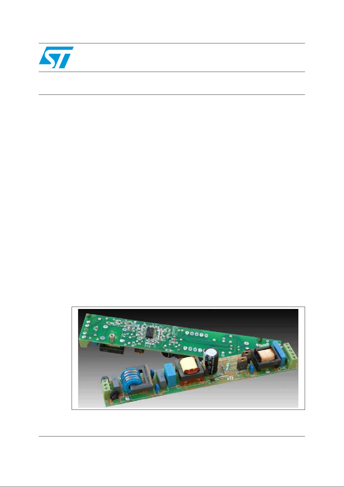
Figure 1. Evaluation board
May 2007 Rev 1 1/11
www.st.com
Page 2

Contents AN2524
Contents
1 Application specifications . . . . . . . . . . . . . . . . . . . . . . . . . . . . . . . . . . . . 3
2 Board performances . . . . . . . . . . . . . . . . . . . . . . . . . . . . . . . . . . . . . . . . . 8
3 Protections . . . . . . . . . . . . . . . . . . . . . . . . . . . . . . . . . . . . . . . . . . . . . . . . . 8
3.1 3.1 PFC over-voltage . . . . . . . . . . . . . . . . . . . . . . . . . . . . . . . . . . . . . . . . . 8
3.2 PFC open loop (feedback disconnection) . . . . . . . . . . . . . . . . . . . . . . . . . 9
3.3 Choke saturation . . . . . . . . . . . . . . . . . . . . . . . . . . . . . . . . . . . . . . . . . . . . 9
3.4 Ignition voltage increase . . . . . . . . . . . . . . . . . . . . . . . . . . . . . . . . . . . . . . . 9
3.5 Lamp power increase . . . . . . . . . . . . . . . . . . . . . . . . . . . . . . . . . . . . . . . . 10
3.6 Lamp disconnection . . . . . . . . . . . . . . . . . . . . . . . . . . . . . . . . . . . . . . . . . 10
4 Revision history . . . . . . . . . . . . . . . . . . . . . . . . . . . . . . . . . . . . . . . . . . . 10
2/11
Page 3

AN2524 Application specifications
1 Application specifications
This board has been designed in order to drive a T5 54W lamp with the following
characteristics:
Table 1. T5 – 54 W lamp characteristics
Input
voltage [V
188 to 264 50 54 400 0.455 120
AC
]
Mains
freq. [Hz]
Lamp
power [W]
Nom. Ignition
voltage [V]
Lamp
current [A]
Lamp
voltage [V]
The board performs the lamp control in all operating phases as well as a PF pre-regulator
stage. It also provides the following protections:
● PFC over voltage;
● PFC feedback disconnection;
● PFC choke saturation
● Lamp disconnection;
● Half-bridge anti-capacitive mode;
● High filament detection
Table 2. Schematic and part list
Ref. Value
BR1 DF06S
R1, R2 3.6 M
R3, R4 910 K
R6 42.2 K
R9 13.3 K
R10, R11 820 K
R12 1.2 M
R13 47
R14 47 K
R15 62 k
R16 56 k
R17, R18 47
R19 0.82, 1 W
R20 10
R22 0.82, 1/2 W
R23 330
R26, R27 680 K
R30, R33 240 K
3/11
Page 4

Application specifications AN2524
Table 2. Schematic and part list (continued)
Ref. Value
R35 1 Mohm
R36, R37 510 K
R38 12 K
R5, R8, R24, R25, R34 n.c.
R7, R21, R28, R29 short
C1 22 µF, 450 V, EPCOS B43888A5226M9
C2, C19, C23 10 nF
C3 n.c.
C4 470 nF
C5 680 nF
C6, C7 1 nF, 1 KV
C8 330 nF
C9 470 nF, 630 V, EPCOS B32652
C10 4.7 nF, 2 kV EPCOS B32653
C11 1 nF, 630 V
C12 470 pF
C13 100 nF, 250 V
C13b short
C14, C15 100 nF, X2, 275 Vac, EPCOS
C16, C17 100 nF
C18 10 µF, 35 V
C20 1 nF
C24 330 nF
C21, C22 n.c.
T1 E25, 2.1 mH, EPCOS B78313P7580A005 (T2363 51-03)
T2
F1 2 A fuse
RT1 NTC, 16R
D1 STTH1L06
D2 1N4148
D3 1N4148
D4 1N4148
D5 BZX84C15ZTX
L1 ITACOIL, 1.3 mH
39 mH, EPCOS
B82731M2601A 30
4/11
Page 5

AN2524 Application specifications
Table 2. Schematic and part list (continued)
Ref. Value
Q1 STP4NK50ZD
Q2 STP4NK50ZD
Q3 STD3NK50Z-1
Q4 BC817
IC1 L6585D
Figure 2. Evaluation board schematic
5/11
Page 6

Application specifications AN2524
The PFC section provides the downstream half-bridge with a regulated output voltage of
429 V, defined by the feedback divider connected to the pin INV according to the following
formula:
Equation 1
where V
R1 R2+
V
OUTVREF
is the 2.5 V ref erence internally connecte d to the non in v erting input of the error
REF
⎛⎞
1
--------------------- -+
• 2.5 1
⎝⎠
R6
3.6M 3.6M+
⎛⎞
---------------------------------+
⎝⎠
42.2K
429V=•==
amplifier.
A 100 Hz ripple (twice the mains frequency) is superimposed on the regulated output
voltage. The amplitude of this ripple is determined by the capacitance value of the PFC
output capacitor, namely:
Equation 2
P
∆V
----------------------------------------------------------------- -
OUT
4 π• fL• V
OUT
• C
OUT
•
10V≈=
OUT
where ∆V
output (58 W), f
is one-half of the peak-to-peak ripple, P
OUT
the mains frequency, V
L
the PFC output DC voltage and C
OUT
the estimated power at PFC
OUT
OUT
the bulk
capacitor (22 µF).
To define the power that the PFC stage is able to ha ndle, a sense resistor is connected
between the Power MOSFET source and ground. Its value has been chosen supposing a
global efficiency of 87%. This corresponds to an input power of 62 W leading to a choke
(and Power MOSFET) peak current of 0.93 A at the minimum input voltage. The sense
resistor value causes a maximum peak current of 1V/Rsns so, for a safe proper design, the
saturation current of the PFC inductance must be at least equal to this value. The L6585D
contains an anti-saturation circuit in order t o a v oid this kind of failure that could damage the
PFC Power MOSFET due to high current spikes.
Using the multiplier family characteristic curves (Figure 3), it is possible to fix the operating
point in the worst case condition, th at is minimum input v olta ge and maximum load (poi nt A).
As a result, a resistor of 0.82Ω has been chosen.
Figure 3. Multiplier characteristics
V
CS
1
0.8
0.6
0.4
0.2
4.2V
4V 3.8V
3.6V
3.4V
A
3.2V
3V
2.8V
2.6V
V
COMP
0
0.5 1 1.5 2 2.5 3 3.5
6/11
V
MULT
Page 7

AN2524 Application specifications
The minimum switch ing frequency is set at 34 KHz. This v alue can be obtaine d by u sing the
following formula:
Equation 3
2
where V
IN(RMS)
V
IN RMS()
F
SW MIN()
------------------------------------------------------------------------------------------------ -
is the min/max input voltage, L the inductance value and PIN the input
V
OUT
• V
2L• P
IN
2V
•
•–()•
IN RMS()
OUT
34kHz==
power. This value mu st be h igher than the sta rter frequency whose maximum value is
15 KHz. The RMS current flowing thr ough th e Power MOSFET is equal to ~270 mA and the
STP3NK50 has been chosen consequently.
● Half-bridge section
The lamp pre-heating and run frequency are set at:
Equation 4
F
-----------------------------------------------------------------
PRE
C
OSCRRUNRPRE
k
||
()•
1.328
------------------------------------------------ -
C
12R16
||
()•
R
15
92.77kHz===
Equation 5
F
RUN
k
------------------------------------ -
•
C
OSCRRUN
1.328
-------------------------
C12R16•
50.4kHz===
The pre-heating time duration is defined according to the following formula:
Equation 6
T
PRETCHTDISCH
C
-------- -
I
CH
5
4.63 R
• In
12C5
⎛⎞
•+•=+=
⎝⎠
4.63
-----------
1.5
where I
is the output current on pin TCH just after the start-up, 4.63 V and 1.5 V are the
CH
charge and discharge threshold respectively (see datasheet electrical characteristics). The
frequency shift during ignition is steered by the time constant R
. Figure 4 shows the
15-C8
lamp current during the turn-on sequence (pre-heating → ignition → run mode) together with
the T
and EOI signals that manage the time durations of the different phases.
CH
Figure 4. Pre-heating and ignition sequence
LAMP CURRENT
EOI
Tch
7/11
Page 8
Board performances AN2524
A RMS current equal to ~500 mA flo ws th rough each o f the half-b ridge Power MOSFET and
two STP4NK50Z have been chosen consequently.
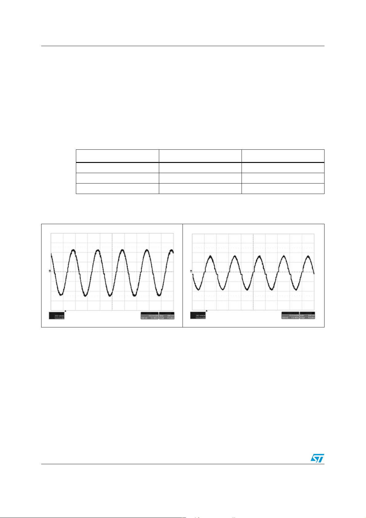
2 Board performances
The PFC section operates in transition mode. The results in terms of PF and THD are
shown in the following table:
Table 3. PF and THD values as a function of the input voltage
Vin [Vac] PF THD [%]
188 0.996 4.5
235 0.990 5.4
264 0.982 7.1
Figure 5. Input current at input voltage equal
to 188 V
AC
3 Protections
3.1 3.1 PFC over-voltage
A resistive divider connected to the HV o utput bus sets the maximum allowed voltage at the
PFC output at 468 V. This value can be obtained by the following formula:
Figure 6. Input current at input voltage equal
to 264 V
AC
Equation 7
V
OVVTHOV
8/11
R3 R4+
⎛⎞
1
--------------------- -+
• 468V==
⎝⎠
R9
Page 9

AN2524 Protections
where V
device stops the PF gate driver until the V
hysteresis (3.26 V typ.).
The above comparator is helpful in stopping the PF gate driver before the PFC output
voltage reaches v alues that could exceed the maximum bulk capacitor voltage or the
mosfets breakdown.
is the threshold of the comparator available at the CTR pin (3.4 V typ.). The
THOV
signal goes below the low threshold
THOV
3.2 PFC open loop (feedback disconnection)
If instead the over-voltage is due to feedback disconnection (R1+R2 fails open), these two
structures work together. In fa ct if the V
voltage falls belo w 1.2 V, typ. (due to the f act that the E/A source capability is limited), the IC
stops in a latched condition.
The CTR pin offers another comparator that is triggered when the pin voltage falls below
0.75 V (typ.). This is a not latched condition that could be used for several purposes (relamp, disab le…). Note that this function offers comp lete protection against not only feedba ck
loop failures or erroneous settings, but also against a failure of the protection itself. Either
resistor of the CTR divider failing short or open or a CTR pin floating results in shutting down
the IC and stopping the pre-regulator.
threshold is crossed and simultaneo usly the INV
OVP
3.3 Choke saturation
The current sense pin voltage is not only sent to the PWM comparator (responsible for
normal Power MOSFET turn-off) b ut also to a se cond compar a tor, whose threshold is 1.7 V
(typ.), and whose function is to det ect choke saturation.
The sense resistor chosen (0.82 Ω), limits the current saturation at 2.1 A (typ.)
3.4 Ignition voltage increase
By placing a resistor between the half-bridge low side and g round and sending its v oltage to
the pin HBCS it is possible to limit the maximum voltage that can be applied to the lamp
during ignition phase (to limit component stress) as well as the minimum switching
frequency (in order to avoid capacitive mode).
With the selected value for R19 (0.82), the resulting maximum voltage is around 680 V.
If the lamp fails ig niti on, t he ballast app lies t o it t he above v oltag e for a duration equal to the
pre-heating time. If, after this time the lamp has not yet ignited, the IC enters low
consumption mode and waits f or either a re -lamp or a Mains re moval before enabling a new
pre-heating /ignition sequence.
9/11
Page 10

Revision history AN2524
3.5 Lamp power increase
If, during run mode, the current fl owing through the lamp increases such that the voltage
across the half-bridge sense resistor exceeds the low threshold of the HBCS pin (910 mV
typ), the L6585D reacts by increasing the switching frequency. This implements a current
control structure. The effect of the frequency increase is the lamp power limitation, so the
structure acts like a rough closed loop with a negative feedback (power increase
increase
correspondence of level crossing, but a frequency correction proportional to how much the
threshold lev el has been cr ossed. Th is protect ion can face the effect appearing at lamp endof-life known as symmetrical rectification.
→ switching frequency increase → power limitation). There is not a switch-off in
→ current
3.6 Lamp disconnection
The circuit built by R35, R37, R38, C24, Q4 monitors the presence/integrity of the high
filament of the lamp . In case of la mp disconnection , the base of t he transistor Q4 is f orced to
ground so through the network R35-D2, the pin EOL-R is forced above the re-lamp
comparator threshold. As the lamp is inserted, Q4 is turned-on and D is reverse-biased so
the voltage at pin EOL-R is no longer affected.
● Rectifying effect (end-of-life)
By means of R30 (240 KΩ ), the window comparator is set to:
– reference in tracking to CTR pin;
– window amplitude equal to 220 mV.
The resistive divider built by R3+R4 and R9 sets CTR voltage under normal condition at
2.9 V. The divider R26+R27 and R31 sets the voltage at pin EOLR at 2.9 V.
The rectifying effect causes a shift (either positive or negative) of the lamp voltage that, in
turn, also shifts the DC component of the block capacitor (C13) voltage. As this value exits
from the allowed window for a time longer than ~1s (equal to preheat time), the IC stops.
4 Revision history
Table 4. Revision history
Date Revision Changes
09-May-2007 1 First issue
10/11
Page 11

AN2524
Please Read Carefully:
Information in this document is provided solely in connection with ST products. STMicroelectronics NV and its subsidiaries (“ST”) reserve the
right to make changes, corrections, modifications or improvements, to this document, and the products and services described herein at any
time, without notice.
All ST products are sold pursuant to ST’s terms and conditions of sale.
Purchasers are solely res ponsibl e fo r the c hoic e, se lecti on an d use o f the S T prod ucts and s ervi ces d escr ibed he rein , and ST as sumes no
liability whatsoever relati ng to the choice, selection or use of the ST products and services described he rein.
No license, express or implied, by estoppel or otherwise, to any intellectual property rights is granted under this document. If any part of this
document refers to any third pa rty p ro duc ts or se rv ices it sh all n ot be deem ed a lice ns e gr ant by ST fo r t he use of su ch thi r d party products
or services, or any intellectua l property c ontained the rein or consi dered as a warr anty coverin g the use in any manner whats oever of suc h
third party products or servi ces or any intellectual property contained therein.
UNLESS OTHERWISE SET FORTH IN ST’S TERMS AND CONDITIONS OF SALE ST DISCLAIMS ANY EXPRESS OR IMPLIED
WARRANTY WITH RESPECT TO THE USE AND/OR SALE OF ST PRODUCTS INCLUDING WITHOUT LIMITATION IMPLIED
WARRANTIES OF MERCHANTABILITY, FITNESS FOR A PARTICUL AR PURPOS E (AND THEIR EQUIVALE NTS UNDER THE LAWS
OF ANY JURISDICTION), OR INFRINGEMENT OF ANY PATENT, COPYRIGHT OR OTHER INTELLECTUAL PROPERTY RIGHT.
UNLESS EXPRESSLY APPROVED IN WRITING BY AN AUTHORIZED ST REPRESENTATIVE, ST PRODUCTS ARE NOT
RECOMMENDED, AUTHORIZED OR WARRANTED FOR USE IN MILITARY, AIR CRAFT, SPACE, LIFE SAVING, OR LIFE SUSTAINING
APPLICATIONS, NOR IN PRODUCTS OR SYSTEMS WHERE FAILURE OR MALFUNCTION MAY RESULT IN PERSONAL INJ URY,
DEATH, OR SEVERE PROPERTY OR ENVIRONMENTAL DAMAGE. ST PRODUCTS WHICH ARE NOT SPECIFIED AS "AUTOMOTIVE
GRADE" MAY ONLY BE USED IN AUTOMOTIVE APPLICATIONS AT USER’S OWN RISK.
Resale of ST products with provisions different from the statements and/or technical features set forth in this document shall immediately void
any warranty granted by ST fo r the ST pro duct or serv ice describe d herein and shall not cr eate or exten d in any manne r whatsoever , any
liability of ST.
ST and the ST logo are trademarks or registered trademarks of ST in various countries.
Information in this document su persedes and replaces all information previously supplied.
The ST logo is a registered trademark of STMicroelectronics. All other names are the property of their respective owners.
© 2007 STMicroelectronics - All rights reserved
STMicroelectronics group of compan ie s
Australia - Belgium - Brazil - Canada - China - Czech Republic - Finland - France - Ger many - Hong Kong - India - Israel - Italy - Japan -
Malaysia - Malta - Morocco - Singapore - Spain - Sweden - Switzerland - United Kingdom - United States of America
www.st.com
11/11
 Loading...