

Page 1
AN2521
Application note
19 V - 75 W laptop adapter with tracking boost PFC
pre-regulator, using the L6563 and L6668
Introduction
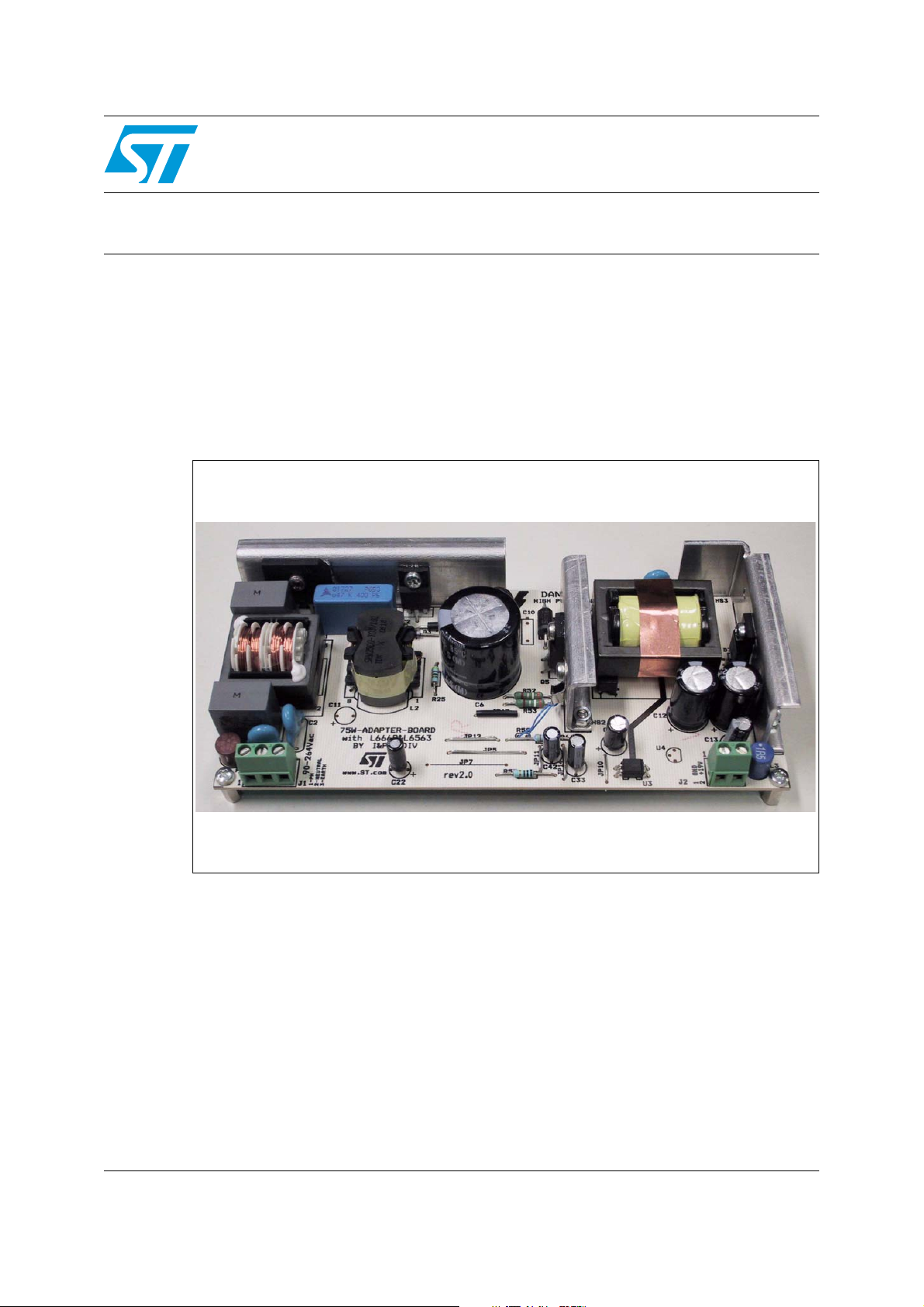
This application note describes the characteristics and features of a 75 W wide range input
mains and power-factor-corrected ac-dc adapter evaluation board. Its electrical specification
is tailored to a typical high-end portable computer power adapter. The distinctive attributes
of this design are the very low standby input consumption (< 0.3 W at 265 V), the excellent
global efficiency (> 85%) for a two stage architecture and the low cost.
Figure 1. L6668 and L6563-75W adapter evaluation board (EVAL6668-75W)
October 2007 Rev 1 1/33
www.st.com
Page 2

Contents AN2521
Contents
1 Main characteristics and circuit description . . . . . . . . . . . . . . . . . . . . . 4
2 Test results . . . . . . . . . . . . . . . . . . . . . . . . . . . . . . . . . . . . . . . . . . . . . . . . 8
2.1 Efficiency measurements at full load, tracking boost option (TBO) . . . . . . 8
2.2 Harmonic content measurement . . . . . . . . . . . . . . . . . . . . . . . . . . . . . . . 11
3 Functional check . . . . . . . . . . . . . . . . . . . . . . . . . . . . . . . . . . . . . . . . . . . 13
3.1 Normal operation . . . . . . . . . . . . . . . . . . . . . . . . . . . . . . . . . . . . . . . . . . . 13
3.2 Standby and no-load operation . . . . . . . . . . . . . . . . . . . . . . . . . . . . . . . . 14
3.3 Over current and short circuit protection . . . . . . . . . . . . . . . . . . . . . . . . . 16
3.4 Overvoltage and open loop protection . . . . . . . . . . . . . . . . . . . . . . . . . . . 18
4 EVAL6668-75W: thermal map . . . . . . . . . . . . . . . . . . . . . . . . . . . . . . . . . 20
4.1 Thermal protection . . . . . . . . . . . . . . . . . . . . . . . . . . . . . . . . . . . . . . . . . . 20
4.2 Thermal map . . . . . . . . . . . . . . . . . . . . . . . . . . . . . . . . . . . . . . . . . . . . . . 20
5 Conducted emission pre-compliance test . . . . . . . . . . . . . . . . . . . . . . 22
6 Bill of material . . . . . . . . . . . . . . . . . . . . . . . . . . . . . . . . . . . . . . . . . . . . . 23
7 PFC coil specification . . . . . . . . . . . . . . . . . . . . . . . . . . . . . . . . . . . . . . . 28
7.1 General description and characteristics . . . . . . . . . . . . . . . . . . . . . . . . . . 28
7.2 Electrical characteristics . . . . . . . . . . . . . . . . . . . . . . . . . . . . . . . . . . . . . . 28
7.3 Electrical schematic and winding characteristics . . . . . . . . . . . . . . . . . . . 28
7.4 Mechanical aspect and pin numbering . . . . . . . . . . . . . . . . . . . . . . . . . . . 29
8 Transformer specification . . . . . . . . . . . . . . . . . . . . . . . . . . . . . . . . . . . 30
8.1 General description and characteristics . . . . . . . . . . . . . . . . . . . . . . . . . . 30
8.2 Electrical characteristics . . . . . . . . . . . . . . . . . . . . . . . . . . . . . . . . . . . . . . 30
8.3 Electrical diagram and winding characteristics . . . . . . . . . . . . . . . . . . . . . 30
8.4 Mechanical aspect and pin numbering . . . . . . . . . . . . . . . . . . . . . . . . . . . 31
9 Revision history . . . . . . . . . . . . . . . . . . . . . . . . . . . . . . . . . . . . . . . . . . . 32
2/33
Page 3

AN2521 List of figures
List of figures
Figure 1. L6668 and L6563-75W adapter evaluation board (EVAL6668-75W) . . . . . . . . . . . . . . . . . . 1
Figure 2. Electrical diagram . . . . . . . . . . . . . . . . . . . . . . . . . . . . . . . . . . . . . . . . . . . . . . . . . . . . . . . . . 7
Figure 3. EVAL6668-75W global efficiency measurements at full load . . . . . . . . . . . . . . . . . . . . . . . . 8
Figure 4. L6563 tracking boost and voltage feed-forward blocks . . . . . . . . . . . . . . . . . . . . . . . . . . . . 9
Figure 5. EVAL6668-75W PFC output voltage vs. ac input voltage . . . . . . . . . . . . . . . . . . . . . . . . . 10
Figure 6. PFC efficiency with and without TBO function at full load . . . . . . . . . . . . . . . . . . . . . . . . . 10
Figure 7. Flyback converter efficiency with and without TBO function at full load . . . . . . . . . . . . . . . 10
Figure 8. Comparison between the global efficiency with and without TBO . . . . . . . . . . . . . . . . . . . 11
Figure 9. EVAL6668-75W compliance to EN61000-3-2 standard @230 V, 50 Hz - full load . . . . . . 11
Figure 10. EVAL6668-75W compliance to JEIDA-MITI standard @100 V, 60 Hz - full load . . . . . . . . 11
Figure 11. EVAL6668-75W compliance to EN61000-3-2 standard @230 V, 50 Hz - half load . . . . . 12
Figure 12. EVAL6668-75W compliance to JEIDA- MITI standard @100 V, 60 Hz - half load . . . . . . . 12
Figure 13. EVAL6668-75W input current waveform @100 V, 60 Hz - full load . . . . . . . . . . . . . . . . . . 12
Figure 14. EVAL6668-75W input current waveform @230 V, 50 Hz - full load . . . . . . . . . . . . . . . . . . 12
Figure 15. EVAL6668-75W flyback stage waveforms @115 V, 60 Hz-full load. . . . . . . . . . . . . . . . . . 13
Figure 16. EVAL6668-75W flyback stage waveforms @230 V, 50 Hz-full load. . . . . . . . . . . . . . . . . . 13
Figure 17. Adapter circuit primary side waveforms 265 V, 50 Hz . . . . . . . . . . . . . . . . . . . . . . . . . . . . 14
Figure 18. EVAL6668-75 W no-load operation waveforms @90 V, 60 Hz . . . . . . . . . . . . . . . . . . . . . 14
Figure 19. EVAL6668-75 W no-load operation waveforms @265 V, 50 Hz . . . . . . . . . . . . . . . . . . . . 14
Figure 20. EVAL6668-75 W transition full load-to-no load at 265 V, 50 Hz . . . . . . . . . . . . . . . . . . . . . 15
Figure 21. EVAL6668-75 W transition no load-to-full load at 265 V, 50 Hz . . . . . . . . . . . . . . . . . . . . . 15
Figure 22. EVAL6668-75 W short circuit at full load & 230 Vac-50 Hz . . . . . . . . . . . . . . . . . . . . . . . . 17
Figure 23. EVAL6668-75 W short circuit removal at full load & 230 Vac-50 Hz . . . . . . . . . . . . . . . . . 17
Figure 24. EVAL6668-75 W short circuit at no-load & 230 Vac-50 Hz . . . . . . . . . . . . . . . . . . . . . . . . 18
Figure 25. EVAL6668-75 W short circuit removal at no-load & 230 Vac-50 Hz. . . . . . . . . . . . . . . . . . 18
Figure 26. EVAL6668-75W Open loop at 115 Vac-60 Hz - full load . . . . . . . . . . . . . . . . . . . . . . . . . . 19
Figure 27. Thermal map at 115 Vac-60 Hz - full load . . . . . . . . . . . . . . . . . . . . . . . . . . . . . . . . . . . . . 20
Figure 28. Thermal map at 230 Vac-50 Hz - full load . . . . . . . . . . . . . . . . . . . . . . . . . . . . . . . . . . . . . 21
Figure 29. CE peak measure at 100 Vac and full load . . . . . . . . . . . . . . . . . . . . . . . . . . . . . . . . . . . . 22
Figure 30. CE peak measure at 230 Vac and full load . . . . . . . . . . . . . . . . . . . . . . . . . . . . . . . . . . . . 22
Figure 31. Electrical diagram . . . . . . . . . . . . . . . . . . . . . . . . . . . . . . . . . . . . . . . . . . . . . . . . . . . . . . . . 28
Figure 32. Mechanical aspect and pin numbering of PFC coil. . . . . . . . . . . . . . . . . . . . . . . . . . . . . . . 29
Figure 33. Electrical diagram . . . . . . . . . . . . . . . . . . . . . . . . . . . . . . . . . . . . . . . . . . . . . . . . . . . . . . . . 30
Figure 34. Winding position on coil former. . . . . . . . . . . . . . . . . . . . . . . . . . . . . . . . . . . . . . . . . . . . . . 31
Figure 35. Mechanical aspect and pin numbering of flyback transformer . . . . . . . . . . . . . . . . . . . . . . 32
3/33
Page 4

Main characteristics and circuit description AN2521
1 Main characteristics and circuit description
The main characteristics of the SMPS are listed here below:
● Universal input mains range: 90 - 264 Vac, 45 − 65 Hz
● Output voltages: 19 V @ 4 A continuous operation
● Mains harmonics: in accordance with EN61000-3-2 class-D
● Standby mains consumption: less than 0.3 W @ 265 Vac
● Overall efficiency: greater than 85%
● EMI: in accordance with EN55022-class B
● Safety: in accordance with EN60950
● PCB single layer: single side, 70 µm, CEM-1, 78 x 174 mm, mixed PTH/SMT
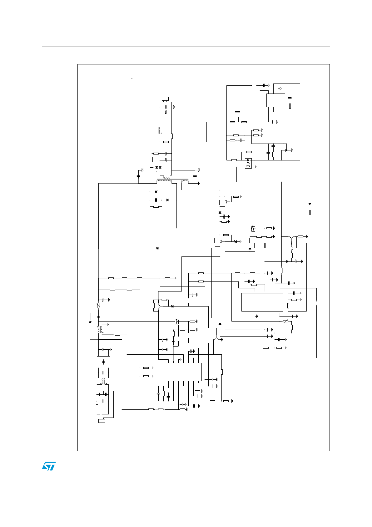
The circuit is made up of two stages: a front-end PFC using the L6563 and a flyback
converter based on the L6668. The electrical schematic is shown in Figure 2.
The flyback stage works as the master stage and therefore is dedicated to controlling circuit
operation, including standby and protection functions. Additionally, it switches the PFC stage
on and off the by means of a dedicated pin on the control IC, thus helping to achieve good
efficiency even at light load. The input EMI filter is a classic Pi-filter, 1-cell for differential and
common mode noise. An NTC in series with the PFC output capacitor limits the inrush
current produced by the charging of the capacitor at plug-in.
The purpose of the PFC stage is to reduce the harmonic content of the input current to be
within the limits imposed by European norm EN61000-3-2. Additionally, it provides a
regulated dc bus used by the downstream converter.
The PFC controller is the L6563 (U1), working in transition mode. It integrates all functions
needed to control the PFC as well as an interface to the master converter. Its power stage
topology is a conventional boost converter, connected to the output of the rectifier bridge. It
includes the coil L2, the diode D3, the capacitor C6 and the power switch Q2, a power
MOSFET.
The secondary winding of L2 (pins 8-3) provides the L6563 with information about the core
demagnetization of the PFC coil, needed by the controller for TM (transition mode)
operation. The divider R7, R12 and R18 provides the L6563 with the instantaneous input
voltage information that is used to modulate the boost current, and to derive additional
information such as the average value of the ac line, which is used by the V
(voltage feed-
FF
forward) function. The divider R2, R6, R8, R9 is dedicated to sensing the output voltage and
feeds the information to the error amplifier, while the divider R3, R5, R11, R19, directly
connected to the output voltage, is dedicated to protecting the circuit in case of voltage loop
failure. To maximize overall efficiency, the PFC makes use of the so-called "tracking boost
option" (TBO). With this function implemented the dc output voltage of the PFC changes
proportionally with the mains voltage. The L6563 achieves this functionality by adding a
resistor (R30) connected to the dedicated TBO pin (#6).
The PFC is switched on and off by a switch (Q1) on the V
pin of the L6563, which is
CC
activated by the PFC-STOP pin of the L6668. The PFC-STOP pin is intended to stop the
PFC controller at light load by cutting its supply. This happens when the COMP pin on the
L6668 controller goes below 2.2V.
The downstream converter, acting as the master stage, is managed by the L6668 IC (U2), a
current mode controller. The 65 kHz nominal switching frequency has been chosen to
4/33
Page 5

AN2521 Main characteristics and circuit description
achieve a compromise between the transformer size and the harmonics of the switching
frequency, thereby optimizing the input filter size and the total solution cost. The power
MOSFET is a standard, inexpensive 800 V component housed in a TO-220FP package,
requiring a small heat sink. The transformer is the layer type, using the standard ferrite core
EER35. The transformer is manufactured by TDK and designed in accordance with
EN60950. The reflected voltage is ~130 V, providing sufficient room for the leakage
inductance voltage spike while maintaining a margin for the reliability of the power MOSFET.
The rectifier D8 and the Transil D4 clamp the peak of the leakage inductance voltage spike
at turn-off of the power MOSFET.
The controller L6668 offers maximum flexibility by integrating all the functionality needed for
high performance SMPS control with a minimum component count. A new feature
embedded in the device is a high voltage current source used at start-up which draws
current directly from the dc bus and charges capacitor C33. After the voltage on C33 has
reached the L6668 turn-on threshold and the circuit starts to operate, the controller is
powered by the transformer via the auxiliary winding and diode D11. After start-up, the HV
current source is deactivated, saving power during normal operation and allowing very good
circuit efficiency during standby.
The L6668 utilizes a Current Mode control system, so the current flowing through the
primary winding is sensed by R52 and R53 and is then fed into pin #12 (ISEN). Resistor
R41 connected between pin #12 (ISEN) and pin #15 (S_COMP) provides the correct slope
compensation to the current signal, necessary for correct loop stability in CCM mode at duty
cycles greater than 50%. The circuit connected to pin #7 (DIS) provides over-voltage
protection in case of feedback network failure, while the thermistor R58 provides for a
thermal protection of the power MOSFET (Q5). This pin is also connected to the
PWM_LATCH pin of the L6563 which is dedicated to stopping activity of the flyback
converter in case of PFC loop failure that could be damaging to the circuit. To definitively
latch this state, the internal circuitry of the L6668 monitors the V
and periodically
CC
reactivates the HV current source to supply the IC. After OVP detection and L6668 Disable
intervention, circuit operation can be resumed only after disconnection of the mains plug.
The switching frequency is programmed by the RC connected to pin #16 (RCT) and in case
of reduced load operation the controller can decrease the operating frequency via pin #13
(STBY) and resistor R42, proportionate with the load consumption. The resistor divider R60
and R61 connected to pin #9 (SKIPADJ) allows setting of the initial L6668 threshold to Burst
Mode functionality when the power supply is lightly loaded. Additional functions embedded
in the L6668 are the programmable soft-start and a 5 V reference, available externally.
Circuit regulation is achieved by modulating the voltage on the COMP pin (#10), by means
of the optocoupler U3. Also connected to the COMP pin is the Q6, Q8, R44, R62, C42 and
D13 network, which is dedicated to driving ISEN over its hiccup mode threshold in case of
overload or short condition. In this case the device will be shut down and its consumption
will decrease almost to pre-start-up level. The device will resume operation as soon as the
V
voltage has dropped below the VCC restart level. Thus a reliable hiccup mode is
CC
invoked until the short is removed. A short on-time and long off-time of the hiccup mode are
obtained allowing the average current flowing in the secondary side components to be kept
at a safe level, avoiding consequent catastrophic failures due to their overheating.
Output regulation is done by means of two loops, a voltage and a current loop working
alternately. A dedicated control IC, the TSM1014, has been used. It integrates two
operational amplifiers and a precise voltage reference. The output signal of the error
amplifiers drives optocoupler SFH617A-4 to transfer the information to the primary side and
achieve the required insulation of the secondary side. The output rectifier D7 is a dual
common-cathode Schottky diode. The output rectifier has been selected according to the
5/33
Page 6

Main characteristics and circuit description AN2521
calculated maximum reverse voltage, forward voltage drop and power dissipation. The
snubber, made up of R14, R66 and C8, damps the oscillation produced by the diode D7. A
small LC filter has been added on the output in order to filter the high frequency ripple.
6/33
Page 7
AN2521 Main characteristics and circuit description
g
Figure 2. Electrical diagram
R55
22R
C36
100N
5
6
8
7
C43
12J2
19V@4A
CON2-IN
C17
100N
100uF-25V YXF
C13
L3
TSL0706 - 1R5-4R3
R20
20K
R22
R015-1W - MSR1
1000uF-25V ZL
R66
3R9
1000uF-25V ZL
C16
R14
3R9
C7
2N2 - Y2
R3
2M2R52M2
R2
1M0-1%
C6
100uF-450V
R1
NTC 10R-S236
D3
STTH2L06
D1
1N4005
3
R4
SRW25CQ-T03H102
L2
6 5
+
D2
~
GBU4J
L1
HF2826-253Y1 R2-T01
F1
FUSE 4A
J1
INPUT CONN.
68K
8
C5
470N-400V
_
~
C4
470NF-X2
C2
2N2
C1
2N2
C3
470NF-X2
123
R11
2M2
R6
1M0-1%
R9
R8
C12
D7
C8
1N0-200V
STPS20H100CFP
10-11
15-16
2-3
D4
1.5KE250A
D8
STTH10 8A
C10
RES
R13
RES
D5
BZV55-B30
R19
36K
R16
10K
Q1
BC857C
C11
RES
C14
220N
U1
L6563
C9
100N
R15
RES
R12
3M3
D9
R21
RES
D6
RES
14
VCC
INV1COMP2MULT3CS4VFF5TBO6PFC-OK
R17
C15
R10
RES
75K-1%
75K-1%
R7
3M3
C24
2N2 - Y2
T1
SRW32EC-T01H114
5-6
R35
D11
R72
0R0
R32
RES
R31
4K7
C22
2u2-25V
R28
2K2
BZV55-C8V2
Q2
STP9NK50ZF P
R27
0R33
R29
RES
R24
100K
R25
470R
R23
27R
C20
10N
13
GD
62K
1uF
9
10
12
11
ZCD
RUN
GND
PWM-STOP
C19
2N2
C21
470N
R18
51K
D10
Q3
8
PWM-LATCH
C26
22N
7
R30
22K
C25
220PF
C23
RES
R26
120K
R69
1K0
R67
6K2-1%
R68
120K-1%
R39
56K-1%
R40
RES
C29
RES
R45
2K2
R36
1K8
12
43
U3
SFH617A-4
C28
RES
R38
2R7
BAV103
LL4148
RES
RES
Q4
RES
C27
47uF-50V
R73
62K
R71
RES
D15
RES
R43
Q7
RES
R33
10K
R34
270K
4R7
D12
LL4148
R37
10K-1%
2N2-5%
C30
15
16
RCT
U2
L6668
HV1HVS2GND3OUT4VCC5N.C.6DIS
VCC
CC_OUT
U5
V_REF
1
2
R49
24K-1%
R48
4K7-1%
C31
RES
Q5
STP10NK80ZFP
R53
0R39
R52
0R39
R47
100K
R46
47R
R51
2K2
C34
100PF
R42
8K2
R41
10K
11
14
12
13
SS
ISEN
STBY
S_COMP
PFC_STOP
C33
22uF-50V
C32
100N
R50
1K0
2N2
GND
CV_OUT
TSM1014
CV-
CC+3CC-
4
R65
22K
C44
100N
C35
270N
U4
R54
47K
TS3431IZ-RES
D14
LL4148
R64
43K-1%
Q6
BC857C
R44
47K
Q8
BC847C
R62
3K3
C42
10uF-50V
D13
LL4148
R57
100R
C37
82N
C39
4N7
9
10
COMP
7
C41
10N
SKIP_ADJ
R61
33K
R60
56K
VREF
8
C40
100N
R58
M57703
R59
24K
C38
470PF
OTP PROT
R56
4K7-1%
JP7
RES
1 2
90-264Vac
7/33
Page 8
Test results AN2521
2 Test results
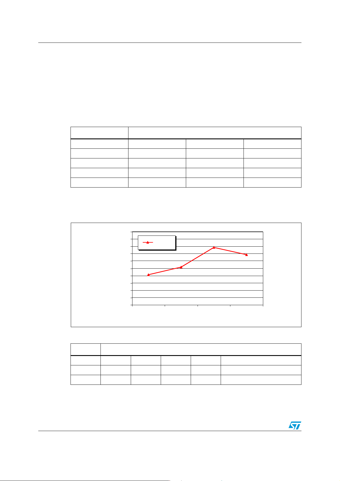
2.1 Efficiency measurements at full load, tracking boost option (TBO)
The following table and diagrams show the single converter and overall efficiency measured
at different input voltages. These measurements are performed with nominal load (4 A).
Table 1. Efficiency measurements at full load using the TBO function
Vin
ac
Efficiency
PFC dc-dc Global
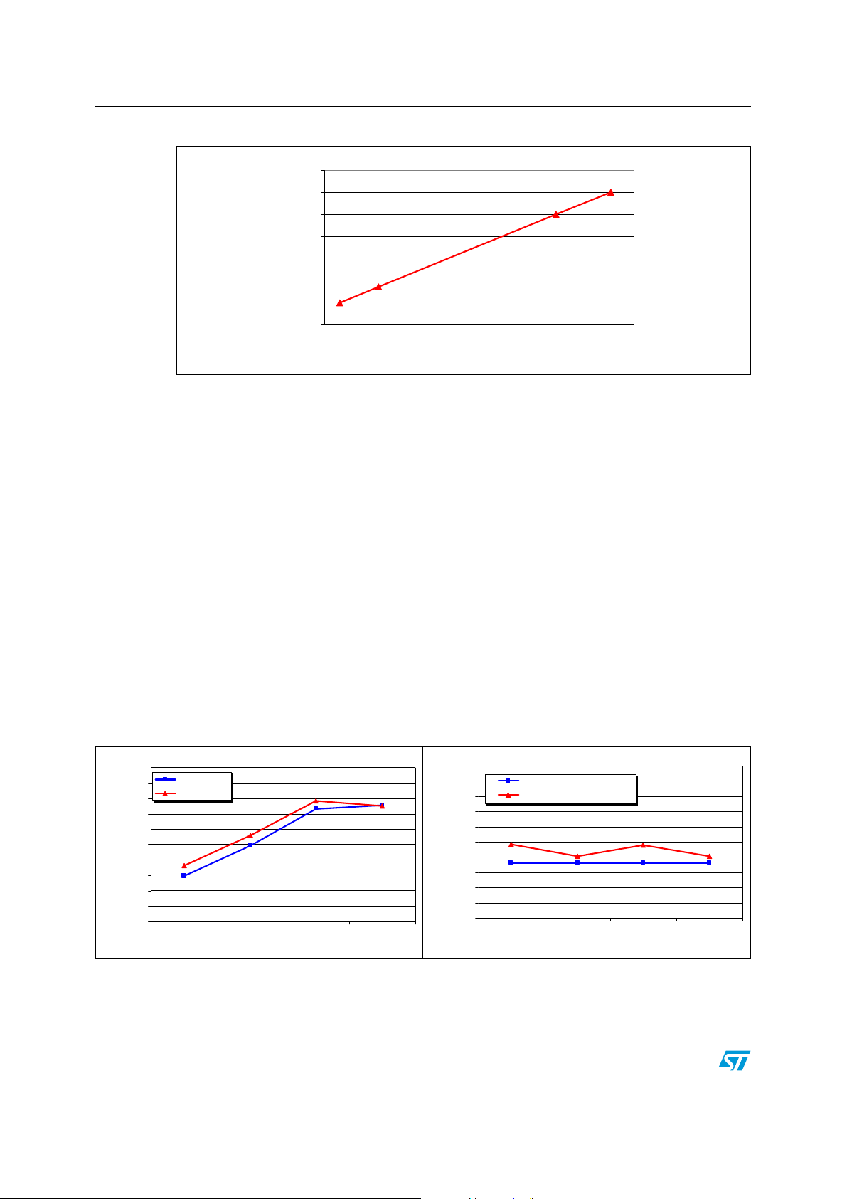
90 [V] 93.63% 89.83% 84.11%
115 [V] 95.62% 89.07% 85.17%
230 [V] 97.84% 89.81% 87.87%
265 [V] 97.53% 89.06% 86.86%
1. Compliant to CEC, EU-COC, regulation. In Table 1 and Figure 3 the single converter efficiency
measurement is shown. Thanks to the very good efficiency of any single block the overall efficiency is very
high too, especially if we compare this data with similar converters using a double stage and a flyback
topology as downstream converter.
Figure 3. EVAL6668-75W global efficiency measurements at full load
90%
89%
88%
87%
86%
85%
84%
83%
82%
OVERALL EFFICIENCY
81%
80%
WITH TBO
90 115 230 265
Vin [Vrms]
(1)
(1)
Table 2. ENERGY STAR compliance
Vin
ac
115 [V] 85.26% 86.32% 86.28% 85.17% 85.75%
230 [V] 83.4% 85.2% 86.74% 87.87% 85.8%
1 A 2 A 3 A 4 A Average
In Ta bl e 2 the ENERGY STAR efficiency measurements are shown. The average of the two
mains voltage inputs in four different load conditions is compliant with the target requirement
(better than 84%).
8/33
ENERGY STAR efficiency
Page 9
AN2521 Test results
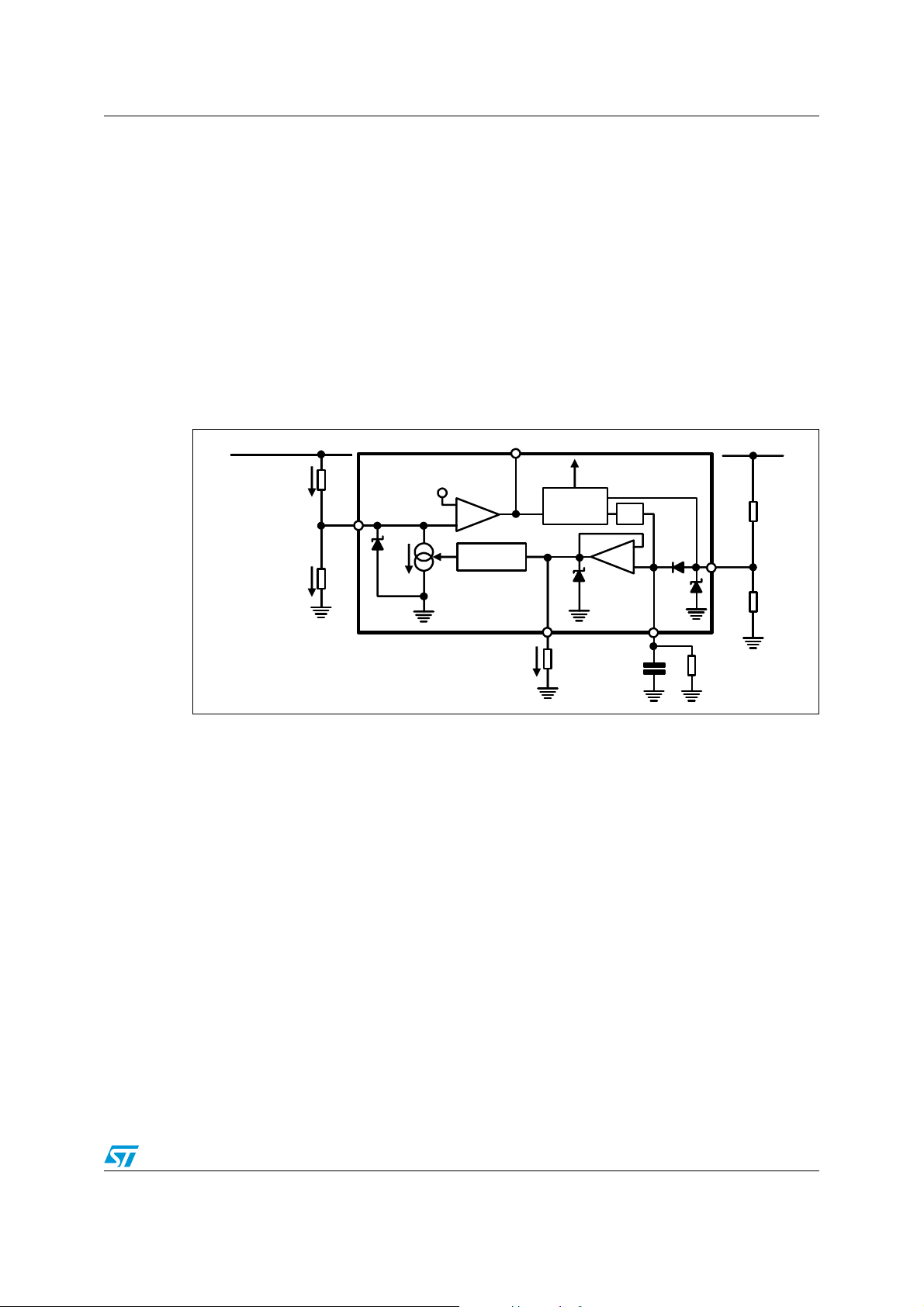
To achieve optimal efficiency the PFC stage implements the tracking boost function. It
consists of a PFC output voltage that follows the input voltage. Typically, in traditional PFC
stages, the dc output voltage is regulated at a fixed value (typically 400 volts) but in some
applications, such as this one using a flyback as the downstream converter, it could be
advantageous to regulate the PFC output voltage with the tracking boost or "follower boost"
approach. In this way the circuit with the TBO function provides improved efficiency and,
thanks to the lower differential voltage across the boost inductor, the value of L2 can be
reduced as compared to the same circuit without the TBO function. In the present case a
400 µH inductor has been used, while with a fixed output voltage PFC working at a similar
operating frequency, a 700 µH inductor is required.
To achieve the TBO function on the L6563, a dedicated input of the multiplier is available on
TBO pin #6. This function can be implemented by simply connecting a resistor (RT) between
the TBO pin and ground.
Figure 4. L6563 tracking boost and voltage feed-forward blocks
Vout
COM
IR
R1
INV 1
I
R
R2
9.5V
I
TBO
2.5V
+
E/A
-
CURRENT
2
1:1
L6563
L6563A
ITBO
current
reference
MULTIPLIER
3V
6
TBO
R
T
1/V
2
"ideal"
-
diode
+
9.5V
5
VFF
CF
Rectified mains
R5
3
MUL
R6
RF
The TBO pin presents a dc level equal to the peak of the MULT pin voltage and is then
representative of the mains RMS voltage. The resistor defines the current, equal to
V(TBO)/RT, which is internally mirrored 1:1 and sunk from the INV pin (pin 1) input of the
error amplifier. In this way, when the mains voltage increases, the voltage at the TBO pin will
increase as well, and so will the current flowing through the resistor connected between
TBO and GND. A larger current will then be sunk by the INV pin and the output voltage of
the PFC pre-regulator will be forced higher. Obviously, the output voltage will move in the
opposite direction if the input voltage decreases.
To avoid an unwanted rise in output voltage should the mains voltage exceed the maximum
specified value, the voltage at the TBO pin is clamped at 3 V. By properly selecting the
multiplier bias it is possible to set the maximum input voltage above which input-to-output
tracking ends and the output voltage becomes constant. If this function is not used, the pin
should be left open; the device will regulate at a fixed output voltage.
9/33
Page 10
Test results AN2521
Y
Y
Figure 5. EVAL6668-75W PFC output voltage vs. ac input voltage
417
384
351
318
285
252
219
PFC OUTPUT VOLTAGE [V]
186
80 130 180 230 280
242
218
Vin [Vrms]
351
384
In Figure 5 we can see that the PFC output voltage variation vs. the ac input voltage (i.e. the
input voltage for the flyback stage) is dependent on the input mains voltage, but its range is
narrower than a wide range input. Thus the design of the flyback converter is not completely
optimized as with a standard PFC delivering a stable 400 V output, but its design is much
simpler than that of a wide range flyback. Additionally, the PFC converter using the TBO,
with its lower differential voltage across the inductor and lower current ripple, will have lower
RMS current and therefore better efficiency at low mains, where normally the efficiency of
typical PFCs is lower. The result is a global efficiency of the circuit that will be higher than
that of a fixed output voltage one circuit, especially at lower mains. Most of the power
dissipation will not be concentrated on the PFC only but will be shared with the flyback.
Therefore, there will not be thermal hotspots and the reliability of the circuit will be improved.
This is confirmed in the diagram in Figure 6, where the efficiency of the PFC has been
measured both with the active TBO function and without it. As shown, at low input mains the
circuit has an efficiency improvement better than 2 percent. As the input mains voltage
increases the switching losses become more significant and the fixed output voltage PFC
appears more efficient.
Figure 6. PFC efficiency with and without
TBO function at full load
100%
PFC STAGE EFFICIENC
99%
98%
97%
96%
95%
94%
93%
92%
91%
90%
WITHOUT TBO
WITH TBO
90 115 230 265
Vin [Vrms]
Using the TBO function even the flyback converter efficiency is very good, as shown in
Figure 7 where it is compared with the efficiency of the same converter powered by a fixed
Figure 7. Flyback converter efficiency with
and without TBO function at full
load
95%
94%
93%
92%
91%
90%
89%
88%
87%
86%
85%
FLYBACK STAGE EFFICIENC
400 Vdc FIXED I/P VOLTAGE
WITH TBO
90 115 230 265
Vin [Vrms]
10/33
Page 11

AN2521 Test results
O
400 V input voltage. It can be observed that an improvement is achieved at 90 Vac and 230
Vac mains.
As a final measurement, the comparison between the global efficiency with and without
TBO is shown in Figure 8, confirming the previous measurements.
Figure 8. Comparison between the global efficiency with and without TBO
90%
89%
88%
87%
86%
85%
84%
83%
82%
OVERALL EFFICIENCY
81%
80%
WITHOUT TB
WITH TBO
90 115 230 265
Vin [Vrms]
2.2 Harmonic content measurement
One of the main purposes of a PFC pre-conditioner is to correct the input current distortion,
decreasing the harmonic contents below the limits of the relevant regulations. Therefore, the
board has been tested according to the European rule EN61000-3-2 Class-D and Japanese
rule JEIDA-MITI Class-D, at full load and 50% of output rated load, at both nominal input
mains voltages.
As demonstrated in the illustrations below, the circuit is capable of reducing the harmonics
well below the limits of both regulations from full load down to light load. Because the
maximum input power of the board is close to the limit of 75 W, to demonstrate the correct
behavior of the circuit it has been tested also a 37 W (half load). Of course, no current
regulation requires meeting any limit at these power levels.
Figure 9. EVAL6668-75W compliance to
EN61000-3-2 standard @230 V, 50
1
0.1
0.01
Hz - full load
Measured value EN61000-3-2 Class -D li m i ts
Figure 10. EVAL6668-75W compliance to
0.1
0.01
JEIDA-MITI standard @100 V, 60 Hz
- full load
Measured value JEIDA-MITI Class-D limits
1
0.001
Harmonic Current [ A]
0.0001
1 3 5 7 9 111315171921232527293133353739
Harmonic Order [n]
0.001
Harmonic Current [A]
0.0001
1 3 5 7 9111315171921232527293133353739
Harmonic Order [n]
11/33
Page 12

Test results AN2521
Figure 11. EVAL6668-75W compliance to
EN61000-3-2 standard @230 V, 50
1
0.1
0.01
0.001
Harmonic Current [A]
0.0001
Hz - half load
Measured value EN61000-3-2 Class-D lim i t s
1 3 5 7 9 111315171921232527293133353739
Harmonic Order [ n]
On the bottom side of each diagram the total harmonic distortion and power factor have
been measured as well. The values in all conditions give a clear idea of the correct
functioning of the PFC even if the tracking boost option has been implemented.
For user reference, input current and voltage waveforms at the nominal input mains voltages
and full load are shown below.
Figure 13. EVAL6668-75W input current
waveform @100 V, 60 Hz - full load
Figure 12. EVAL6668-75W compliance to
JEIDA- MITI standard @100 V, 60 Hz
- half load
Measured value JEIDA-MITI Class-D limits
1
0.1
0.01
0.001
Harmonic Current [A]
0.0001
1 3 5 7 9111315171921232527293133353739
Harmonic O rder [n]
Figure 14. EVAL6668-75W input current
waveform @230 V, 50 Hz - full load
CH1: input mains voltage
CH2: input mains current
12/33
CH1: input mains voltage
CH2: input mains current
Page 13

AN2521 Functional check
3 Functional check
3.1 Normal operation
Figure 15 and Figure 16 display some waveforms of the flyback stage during steady-state
operation of the circuit at full load and nominal input voltage ranges. Under full load
conditions the L6668 switching frequency has been set to 65 kHz in order to achieve good
efficiency and to limit the switching noise.
It's possible to note that the CH3 relevant to the output voltage of the PFC circuit shows the
tracking boost function setting at a different PFC output voltage (247 / 348 volts), which is
dependent on the mains input voltage as mentioned on the previous page.
Figure 15. EVAL6668-75W flyback stage
CH1: input mains voltage
CH2: input mains current
CH3: PFC output voltage
waveforms @115 V, 60 Hz-full load
In Figure 17 the drain voltage waveforms and the measurement of the peak voltage at full
load and maximum mains input voltage are shown.
The maximum voltage peak in this condition is 676 V, which ensures reliable operation of the
power MOSFET with a good margin against the maximum BV
Figure 16. EVAL6668-75W flyback stage
waveforms @230 V, 50 Hz-full load
CH1: input mains voltage
CH2: input mains current
CH3: PFC output voltage
.
DSS
13/33
Page 14

Functional check AN2521
Figure 17. Adapter circuit primary side waveforms 265 V, 50 Hz
CH1: Q7 drain voltage
CH2: L6668 Vpin #12 (ISEN)
3.2 Standby and no-load operation
Figure 18. EVAL6668-75 W no-load operation
waveforms @90 V, 60 Hz
CH1: Q7 drain voltage
CH2: L6668 COMP (pin #10)
CH3: L6668 V
(pin #5)
CC
In Figure 18 and Figure 19, some no-load waveforms of the circuit are shown. As illustrated,
the L6668 works in burst mode to achieve optimal efficiency. The burst mode threshold can
be adjusted by setting the divider connected to the SKIPADJ pin (#9). When the voltage at
the COMP pin falls 50 mV below the voltage on the SKIPADJ pin, the IC is shut down and
consumption is reduced. The chip is re-enabled as the voltage on the COMP pin exceeds
the voltage on the threshold set by pin 9 with its hysteresis. Additionally, in order to achieve
the best efficiency during light load operation the PFC stage is turned off. In fact, the L6668
pin #14 (PFC_STOP) is dedicated to enabling or disabling PFC operation according to the
Figure 19. EVAL6668-75 W no-load operation
waveforms @265 V, 50 Hz
CH1: Q7 drain voltage
CH2: L6668 COMP (pin #10)
CH3: L6668 V
(pin #5)
CC
14/33
Page 15

AN2521 Functional check
output load level. This pin is intended to drive the base of a PNP transistor in systems
including a PFC pre-regulator, to stop the PFC controller at light load by cutting its supply.
Pin #14 (PFC_STOP), while normally low, opens if the voltage on the COMP pin is lower
than 2.2 V, and returns low when the voltage on the COMP pin exceeds 2.7 V. Whenever the
IC is shut down, either latched (DIS > 2.2 V, ISEN > 1.5 V) or not latched (UVLO, SKIPADJ <
0.8), the pin is open as well. In Figure 19, the V
value is also given, showing that the IC is
CC
powered with a good margin with respect to the L6668 turn-off threshold (9.4 V), avoiding
any spurious turn-off possibilities that could affect the output voltage stability.
In Ta bl e 3 , the power consumption from the mains during no-load operation is shown. As
can be observed, thanks to the L6668 standby functionality the input power constantly
remains well below 300 mW. Therefore, all mandatory or voluntary regulations currently
applicable or that will become effective in the near future can be respected using this
chipset.
Table 3. Input power at no-load vs. mains voltage
Vin [Vrms] Input power [W]
90 0.126
115 0.146
230 0.268
265 0.282
(1)
(1)
1. Compliant to CEC, EU-COC, Energy Star
Figure 20. EVAL6668-75 W transition full load-
to-no load at 265 V, 50 Hz
CH1: Q2 drain voltage
CH2: L6668 SOFT START - pin #11
CH3: output voltage
CH4: L6668 V
(pin #5)
CC
In Figure 20 and Figure 21, the transitions from full load to no-load and vice-versa at
maximum input voltage have been checked. The maximum input voltage has been chosen
for the above illustrations because it is the most critical input voltage for transition. In fact, at
no-load, the burst pulses have a lower repetition frequency and the V
restart cycles of the controller. Additionally, there is a wider range variation for the input
Figure 21. EVAL6668-75 W transition no load-
to-full load at 265 V, 50 Hz
CH1: Q2 drain voltage
CH2: L6668 SOFT START - pin #11
CH3: output voltage
CH4: L6668 V
(pin #5)
CC
could drop, causing
CC
15/33
Page 16

Functional check AN2521
voltage to the flyback converter as a result of the PFC turning on or off. As the figures show,
both transitions are clean and there is no output voltage, V
dip or restarting attempt that
CC
could affect proper power supply operation.
The input power consumption of the board has also been checked at light load conditions,
simulating an adapter powering a laptop PC during power-saving operation. The results are
shown in Tab le 4 , 5 and 6 below, where the low load efficiency with standard inputs of 115 V
and 230 V is calculated.
Table 4. Light load efficiency (0.5 W)
Vinac [Vrms] Pout [W] Pin [W] Efficiency
115 0.52 0.75
230 0.52 0.88
1. Compliant to US Executive order 13221 “1W _Standby“
(1)
(1)
68.67%
58.52%
Table 5. Light load efficiency (1.2 W)
Vinac [Vrms] Pout [W] Pin [W] Efficiency
115 1.2 1.55 77.86%
230 1.2 1.71 70.35%
Table 6. Light load efficiency (2.4 W)
Vinac [Vrms] Pout [W] Pin [W] Efficiency
115 2.41 2.93 82.14%
230 2.4 3.14 76.56%
As visible in Ta bl e 4 , 5 and 6, the input power consumption is always very low and the
efficiency remains significantly high even at output power levels where the power supply
efficiency normally drops. This is achieved thanks to the burst mode adjustable threshold of
the L6668 SKIPADJ pin and the PFC management by the PFC_STOP pin, as previously
described.
3.3 Over current and short circuit protection
An important function of any power supply is its ability to survive instances of output
overload or short circuit, avoiding any consequent failure. Additionally, the power supply
must be compliant with safety rules which require that the components will not melt or burnout in fault conditions. It’s common to find circuits with good protection capability against
load shorts but which do not survive dead shorts such as those of an output electrolytic
capacitor or a secondary rectifier, or in cases of transformer saturation. Moreover, in cases
of a shorted rectifier the equivalent circuit changes and the energy are delivered even during
the ON time, as in forward mode. In this evaluation board the over-current is managed by
U5, a CC/CV controller. Inside the IC there is a reference and two Or-end operational
amplifiers, one dedicated to act as the error amplifier of the voltage loop and the other
dedicated to act as the error amplifier of the current loop. If the output current exceeds the
programmed value, the current loop error amplifier takes over and, via the optocoupler,
16/33
Page 17

AN2521 Functional check
controls the voltage at the COMP pin of the L6668, thus regulating the output current. In
case of a dead short, the current cannot be limited effectively by U5 because it will be
unpowered. Therefore, additional, efficient protection circuitry on the primary side will be
needed. In this board the voltage at the ISEN pin of the L6668 is sensed and if it exceeds
the V
controller stops operation and will remain in the OFF state until the voltage across the V
threshold the controller is forced to work in hiccup mode. In this way the
ISENdis
CC
pin decreases to a level below the UVLO threshold. It will then attempt to restart, but without
success if the secondary short has not been removed. This provides a low frequency hiccup
working mode, limiting the current flowing on the secondary side and thus preventing the
power supply from overheating and failing.
Figure 22 shows the circuit behavior during short circuit. Observe that the L6668 stops
switching, the V
voltage drops until it reaches the UVLO threshold. Then the IC
CC
decreases its consumption, thus increasing the duration of the OFF time, and avoiding high
dissipation on the secondary side under short conditions. The soft start capacitor will also
be discharged. At this point, the HV start-up pin recharges the V
capacitor and, as soon
CC
the turn-on threshold is reached, the circuit attempts to restart but it will cease operation
within a few milliseconds, repeating the sequence just described. The restart attempt will be
repeated indefinitely until the short is removed.
Figure 23, instead, shows the sequence of operation in short circuit when the short is
removed. As the figure illustrates, a new start-up sequence takes place and the circuit
resumes normal operation after a soft-start cycle.
Figure 22. EVAL6668-75 W short circuit at full
load & 230 Vac-50 Hz
CH1: Q2 drain voltage
CH2: SOFT START voltage - pin #11
CH3: output voltage
CH4: V
CC
Thanks to the TSM1014 and the HV current source of the L6668, the fault protection
sequences described in Figure 22 and Figure 23 do not change significantly for any other
input voltage, above all not in the input voltage range of the board.
Figure 23. EVAL6668-75 W short circuit
removal at full load & 230 Vac-50 Hz
CH1: Q2 drain voltage
CH2: SOFT START voltage - pin #11
CH3: output voltage
CH4: V
CC
The protection described previously works correctly even in cases where the output short is
applied during standby or no load operations. The L6668 protects the circuit via the
sequences that has been described for the full load operation, and the circuit resumes
17/33
Page 18

Functional check AN2521
correct operation when the short is removed. In Figure 24 and Figure 25 both sequences
are captured during 230 Vac operation but they do not change significantly over the input
mains range.
Figure 24. EVAL6668-75 W short circuit at no-
load & 230 Vac-50 Hz
CH1: Q2 drain voltage
CH2: SOFT START voltage - pin #11
CH3: output voltage
CH4: V
CC
Figure 25. EVAL6668-75 W short circuit
removal at no-load & 230 Vac-50 Hz
CH1: Q2 drain voltage
CH2: SOFT START voltage - pin #11
CH3: output voltage
CH4: V
CC
3.4 Overvoltage and open loop protection
The EVAL6668-75W board implements two different open loop protections: one for the PFC
and another for the flyback stage.
The PFC controller L6563 is equipped with an OVP, monitoring the current flowing through
the compensation network and entering the error amplifier (pin COMP, #2). When this
current reaches about 18 µA the output voltage of the multiplier is forced to decrease, thus
reducing the energy drawn from the mains. If the current exceeds 20 µA, the OVP is
triggered (dynamic OVP), and the external power transistor is switched off until the current
falls below approximately 5 µA. However, if the overvoltage persists (e.g. if the load is
completely disconnected), the error amplifier will eventually saturate low, triggering an
internal comparator (static OVP) which will keep the external power switch turned off until
the output voltage returns to a point near the regulated value.
The OVP function described above is capable of handling "normal" overvoltage conditions,
i.e. those resulting from an abrupt load/line change or occurring at start-up. It cannot handle
the overvoltage generated, for instance, when the upper resistor of the output divider fails
open. The voltage loop can no longer read the information on the output voltage and will
force the PFC pre-regulator to work at maximum ON time, causing the output voltage to rise
uncontrollably.
A pin on the L6563 (PFC_OK, #7) has been provided for additional monitoring of the output
voltage with a separate resistor divider (R3, R5, R11 high, R19 low, see Figure 1.and 2).
This divider is selected so that the voltage at the pin reaches 2.5 V if the output voltage
18/33
Page 19

AN2521 Functional check
exceeds a preset value, usually larger than the maximum Vo that can be expected, including
also overshoots due to worst-case load/line transients.
In this case, VO = 400 V, Vox = 460 V. Select: R3 + R5 + R11 = 6.6 MΩ. Three resistors in
series have been chosen according to their voltage rating.
Thus: R19 = 6.6 MΩ · 2.5 / (460-2.5) = 36 kΩ.
When this function is triggered, the gate drive activity is immediately stopped, the device is
shut down, its quiescent consumption is reduced below 250 µA and the condition is latched
as long as the supply voltage of the IC is above the UVLO threshold. At the same time the
pin PWM_LATCH (pin #8) is asserted high. The PWM_LATCH is an open source output
capable of delivering 3.7 V minimum with a 0.5 mA load, intended for tripping a latched
shutdown function of the PWM controller IC in the cascaded dc-dc converter, so that the
entire unit is latched off. To restart the system it is necessary to recycle the input power, so
that the V
voltages of both the L6563 and the PWM controller go below their respective
CC
UVLO thresholds.
The PFC_OK pin doubles its function as a not-latched IC disable: a voltage below 0.2 V will
shut down the IC, reducing its consumption below 1 mA. In this case both PWM_STOP and
PWM_LATCH keep their high impedance status. To restart the IC simply let the voltage at
the pin go above 0.26 V.
Note that this function offers complete protection against not only feedback loop failures or
erroneous settings, but also against a failure of the protection itself. If a resistor in the
PFC_OK divider fails short or open, or the PFC_OK (#7) pin is floating, it will result in the
shutting down of the L6563 and stopping of controller operation of the flyback stage.
Figure 26. EVAL6668-75W Open loop at 115 Vac-60 Hz - full load
An open loop event is captured in Figure 26. Note the protection intervention stopping the
operation of the L6563 and the activation of the PWM_LATCH pin that is connected to the
L6668 pin #7 (DIS). This function of the L6668 is a latched device shutdown. Internally the
pin connects a comparator which shuts the IC down and brings its consumption to a value
just higher than before start-up, when the voltage on the pin exceeds 2.2 V. The information
is latched and it is necessary to recycle the input power to restart the IC. The latch is
removed as the voltage on the V
pin goes below the UVLO threshold.
CC
19/33
Page 20

EVAL6668-75W: thermal map AN2521
The flyback stage is also protected against open loop conditions that lead to loss of control
of the output voltage. A divider connected to the auxiliary winding of the transformer is also
connected to the L6668 pin #7 (DIS) and, in case of excessively high output voltage
resulting from loop failure, provides for the triggering of the internal comparator connected to
that pin. In this case operation of the L6563 will cease because the L6668 will stop the PFC
stage operation via the PFC_STOP pin. The V
by the HV start-up generator of the L6668. To restart the operation, it will be necessary to
unplug and re-plug the mains, to unlatch the L6668.
powering both the ICs will be maintained
CC
4 EVAL6668-75W: thermal map
4.1 Thermal protection
The EVAL6668-75W is also equipped with thermal protection of the flyback's power
MOSFET (Q5). Its temperature is sensed using the NTC thermistor R58 connected to the
L6668 pin #7 (DIS). If the temperature of the heat sink rises above the maximum allowed
level (80 - 85 °C), the threshold of the internal comparator will be exceeded and the L6668
latched as in the case of open loop. To restart the operation of the circuit, it will be
necessary to unplug and re-plug the mains.
4.2 Thermal map
In order to check the reliability of the design, thermal mapping has been performed using an
infrared camera. In Figure 27 and 28, the thermal measurements on the key components at
nominal input voltage are shown. The correlation between the measurement points and
components for both thermal maps is indicated in Tab le 7 below. The ambient temperature
during both measurements was 27 °C. All other components on the board work within the
temperature limits, ensuring reliable long-term operation of the power supply.
Figure 27. Thermal map at 115 Vac-60 Hz - full load
20/33
Page 21

AN2521 EVAL6668-75W: thermal map
Figure 28. Thermal map at 230 Vac-50 Hz - full load
Table 7. Measured temperature table @115 Vac and 230 Vac - full load
Point Component Temperature @115 Vac Temperature @230 Vac
A D2 59.6 °C 52.9 °C
B Q2 59.9 °C 54.0 °C
C D4 101 °C 100 °C
D Q5 75.8 °C 67.2 °C
E T1 - WINDING 76.1 °C 77.7 °C
F T1 – CORE 74.9 °C 76.3 °C
G D7 77.4 °C 75.7 °C
H R1 (NTC) 100 °C 80.5 °C
21/33
Page 22

Conducted emission pre-compliance test AN2521
5 Conducted emission pre-compliance test
The following figures are the peak measurements of the conducted noise emissions at full
load and nominal mains voltages. The limits shown on the diagrams are those of EN55022
Class-B, which are most popular requirements for domestic equipment and imposes less
stringent limits compared to the Class-A, which is dedicated to IT technology equipment. As
visible in the diagrams, in all test conditions there is a good margin for the measurements
with respect to the limits.
Figure 29. CE peak measure at 100 Vac and full load
Figure 30. CE peak measure at 230 Vac and full load
22/33
Page 23

AN2521 Bill of material
6 Bill of material
Table 8. EVAL6668-75W evaluation board: bill of material
Des. Part type/part value Description Supplier
C1 2N2 Y1 safety cap. Murata
C10 Res. Not used
C11 Res. Not used
C12 1000 µF-25V ZL Aluminium ELCAP - ZL series - 105 °C Rubycon
C13 100 µF-25V YXF Aluminium ELCAP - YXF series - 105 °C Rubycon
C14 220NF 50 V CERCAP - general purpose AVX
C15 1 µF 25 V CERCAP - general purpose AVX
C16 1000 µF-25V ZL Aluminium ELCAP - ZL series - 105 °C Rubycon
C17 100N 50 V CERCAP - general purpose AVX
C19 2N2 50 V CERCAP - general purpose AVX
C2 2N2 Y1 safety cap. Murata
C20 10N 50 V CERCAP - general purpose AVX
C21 470N 25 V CERCAP - general purpose AVX
C22 2µ2-25 V Aluminium ELCAP - YXF series - 105 °C Rubycon
C23 Res. Not used
C24
C25 220PF 50 V CERCAP - general purpose AVX
C26 22N 50 V CERCAP - general purpose AVX
C27 47 µF-50 V Aluminium ELCAP - YXF Series - 105 °C Rubycon
C28 Res. Not used
C29 Res. Not used
C3 470N-X2 X2 film CAPACITOR - R46-I 3470--M1- Arcotronics
C30 2N2-5% 50 V - 5% - C0G - CERCAP AVX
C31 Res. Not used
C32 100N 50 V CERCAP - general purpose AVX
C33 22 µF-50 V Aluminium ELCAP - YXF series - 105 °C Rubycon
C34 100PF 50 V CERCAP - general purpose AVX
C35 270N 25 V CERCAP - general purpose AVX
C36 100N 50 V CERCAP - general purpose AVX
C37 82N 50 V CERCAP - general purpose AVX
2N2 - Y1 -
DE1E3KX222M
Y1 safety cap. Murata
C38 470PF 50 V CERCAP - general purpose AVX
23/33
Page 24

Bill of material AN2521
Table 8. EVAL6668-75W evaluation board: bill of material (continued)
Des. Part type/part value Description Supplier
C39 4N7 50 V CERCAP - general purpose AVX
C4 470N-X2 X2 film capacitor - R46-I 3470--M1- Arcotronics
C40 100N 50 V CERCAP - general purpose AVX
C41 10N 50 V CERCAP - general purpose AVX
C42 10 µF-63 V Aluminium ELCAP - SR series - 85 °C Rubycon
C43 2N2 50 V CERCAP - general purpose AVX
C44 100N 50 V CERCAP - general purpose AVX
C5 470N-400 V B32653A4474J - polyprop. film cap EPCOS
C6 100 µF-450 V Aluminium ELCAP - LLS Series - 85 °C NICHICON
C7
C8 1N0-200 V 200 V CERCAP - general purpose AVX
C9 100N 50 V CERCAP - general purpose AVX
D1 1N4005 General purpose rectifier Vishay
D10 LL4148 Fast switching diode Vishay
2N2 - Y1 -
DE1E3KX222M
Y1 safety cap. Murata
D11 BAV103 Fast switching diode Vishay
D12 LL4148 Fast switching diode Vishay
D13 LL4148 Fast switching diode Vishay
D14 LL4148 Fast switching diode Vishay
D15 Res. Not used
D2 GBU4J Single phase bridge rectifier Vishay
D3 STTH2L06 Ultrafast high voltage rectifier STMicroelectronics
D4 1.5KE250A TRANSIL STMicroelectronics
D5 BZV55-B30 ZENER diode Vishay
D6 Res. Not used
D7 STPS20H100CFP High voltage power Schottky rectifier STMicroelectronics
D8 STTH108A High voltage ultrafast rectifier STMicroelectronics
D9 BZV55-C8V2 ZENER diode Vishay
F1 FUSE 4 A Fuse T4A - time delay Wichmann
J1 MKDS 1,5/ 3-5,08 PCB term. block, screw conn., pitch 5MM - 3 W. Phoenix Contact
J2 MKDS 1,5/ 2-5,08 PCB term. block, screw conn., pitch 5mm - 2 W. Phoenix Contact
JP5 Jumper Tinned copper wire jumper
JP7 Res. Tinned copper wire jumper - not used
JP10 Jumper Tinned copper wire jumper
JP11 Jumper Tinned copper wire jumper
24/33
Page 25

AN2521 Bill of material
Table 8. EVAL6668-75W evaluation board: bill of material (continued)
Des. Part type/part value Description Supplier
JP12 Jumper Tinned copper wire jumper
JP13 Jumper Tinned copper wire jumper
JP14 Jumper Tinned copper wire jumper
L1 HF2826-253Y1R2-T01 25 MH-1.2 A input EMI filter TDK
L2 SRW25CQ-T03H112 400 µH PFC inductor TDK
L3 TSL0706 - 1R5-4R3 1 µ5 - radial inductor TDK
Q1 BC857C PNP small signal BJT ZETEX
Q2 STP9NK50ZFP N-channel power MOSFET STMicroelectronics
Q3 Res. Not used
Q4 Res. Not used
Q5 STP10NK80ZFP N-channel power MOSFET STMicroelectronics
Q6 BC857C PNP small signal BJT ZETEX
Q7 Res. not used
Q8 BC847C NPN small signal BJT ZETEX
R1 NTC 10R-S236 NTC resistor 10R - P/N B57236S0100M000 EPCOS
R10 Res. Not used
R11 2M2 - 1% SMD std film res. - 1/4 W - 1% - 100 ppm/°C BC Components
R12 3M3 SMD std film res. - 1/4 W - 1% - 100 ppm/°C BC Components
R13 Res. Not used
R14 3R9 SMD std film res. - 1/4 W - 5% - 250 ppm/°C BC Components
R15 Res. Not used
R16 10 kΩ SMD std film res. - 1/8 W - 1% - 100 ppm/°C BC Components
R17 62 kΩ SMD std film res. - 1/8 W - 5% - 250 ppm/°C BC Components
R18 51 kΩ SMD std film res. - 1/4 W - 5% - 250 ppm/°C BC Components
R19 36 kΩ SMD std film res. - 1/8 W - 1% - 100 ppm/°C BC Components
R101 0R0 SMD std film res. - 1/4 W - 5% - 250 ppm/°C BC Components
R102 0R0 SMD std film res. - 1/4 W - 5% - 250 ppm/°C BC Components
R103 0R0 SMD std film res. - 1/4 W - 5% - 250 ppm/°C BC Components
R104 0R0 SMD std film res. - 1/4 W - 5% - 250 ppm/°C BC Components
R105 0R0 SMD std film res. - 1/4 W - 5% - 250 ppm/°C BC Components
R2 1M0-1% SMD std film res. - 1/4 W - 1% - 100 ppm/°C BC Components
R20 20 kΩ SMD std film res. - 1/4 W - 5% - 250 ppm/°C BC Components
R21 Res. Not used
R22 R015 - 1 W SMD film res. 1 W - 2512 MSR1 MEGGIT
R23 27R SMD std film res. - 1/4 W - 5% - 250 ppm/°C BC Components
25/33
Page 26

Bill of material AN2521
Table 8. EVAL6668-75W evaluation board: bill of material (continued)
Des. Part type/part value Description Supplier
R24 100 kΩ SMD std film res. - 1/8 W - 5% - 250 ppm/°C BC Components
R25 470R SFR25 axial stand. film res. - 0.4 W - 5% - 250 ppm/°C BC Components
R26 120 kΩ SMD std film res. - 1/4 W - 5% - 250 ppm/°C BC Components
R27 0R33 SFR25 axial stand. film res. - 0.4 W - 5% - 250 ppm/°C BC Components
R28 2k2 SMD std film res. - 1/8 W - 5% - 250 ppm/°C BC Components
R29 Res. Not used
R3 2M2 - 1% SMD std film res. - 1/4 W - 1% - 100 ppm/°C BC Components
R30 22 kΩ SMD std film res. - 1/8 W - 5% - 250 ppm/°C BC Components
R31 4k7 SMD std film res. - 1/4 W - 5% - 250 ppm/°C BC Components
R32 Res. Not used
R33 10 kΩ SMD std film res. - 1/4 W - 5% - 250 ppm/°C BC Components
R34 270 kΩ SMD std film res. - 1/8 W - 5% - 250 ppm/°C BC Components
R35 2R7 SMD std film res. - 1/8 W - 5% - 250 ppm/°C BC Components
R36 1k8 SMD std film res. - 1/8 W - 5% - 250 ppm/°C BC Components
R37 10 kΩ - 1% SMD std film res. - 1/8 W - 1% - 100 ppm/°C BC Components
R38 Res. Not used
R39 56 kΩ - 1% SMD std film res. - 1/4 W - 1% - 100 ppm/°C BC Components
R4 68 kΩ SMD std film res. - 1/4 W - 5% - 250 ppm/°C BC Components
R40 Res. Not used
R41 10 kΩ SMD std film res. - 1/8 W - 5% - 250 ppm/°C BC Components
R42 8k2 SMD std film res. - 1/8 W - 5% - 250 ppm/°C BC Components
R43 4R7 SMD std film res. - 1/8 W - 5% - 250 ppm/°C BC Components
R44 47 kΩ SMD std film res. - 1/8 W - 5% - 250 ppm/°C BC Components
R45 2k2 SMD std film res. - 1/8 W - 5% - 250 ppm/°C BC Components
R46 47R SMD std film res. - 1/8 W - 5% - 250 ppm/°C BC Components
R47 100 kΩ SMD std film res. - 1/8 W - 5% - 250 ppm/°C BC Components
R48 4k7 - 1% SMD std film res. - 1/8 W - 1% - 100 ppm/°C BC Components
R49 24 kΩ - 1% SMD std film res. - 1/8 W - 1% - 100 ppm/°C BC Components
R5 2M2 - 1% SMD std film res. - 1/4 W - 5% - 250 ppm/°C BC Components
R50 1k0 SMD std film res. - 1/8 W - 5% - 250 ppm/°C BC Components
R51 2k2 SMD std film res. - 1/8 W - 5% - 250 ppm/°C BC Components
R52 0R39 SFR25 AXIAL std film res. - 0.4 W - 5% - 250 ppm/°C BC Components
R53 0R39 SFR25 axial stand. film res. - 0.4 W - 5% - 250 ppm/°C BC Components
R54 47 kΩ SMD std film res. - 1/8 W - 5% - 250 ppm/°C BC Components
R55 22R SMD std film res. - 1/8 W - 5% - 250 ppm/°C BC Components
26/33
Page 27

AN2521 Bill of material
Table 8. EVAL6668-75W evaluation board: bill of material (continued)
Des. Part type/part value Description Supplier
R56 4k7 - 1% SMD std film res. - 1/8 W - 1% - 100 ppm/°C BC Components
R57 100R SFR25 axial stand. film res. - 0.4 W - 5% - 250 ppm/°C BC Components
R58 M57703 - 10 kΩ 10 k thermistor - B57703M0103G040 EPCOS
R59 24 kΩ SMD std film res. - 1/8 W - 5% - 250 ppm/°C BC Components
R6 1M0 - 1% SMD std film res. - 1/4 W - 1% - 100 ppm/°C BC Components
R60 56 kΩ SMD std film res. - 1/4 W - 5% - 250 ppm/°C BC Components
R61 33 kΩ SMD std film res. - 1/8 W - 5% - 250 ppm/°C BC Components
R62 3k3 SMD std film res. - 1/8 W - 5% - 250 ppm/°C BC Components
R63 0R0 SMD std film res. - 1/4 W - 5% - 250 ppm/°C BC Components
R64 43 kΩ - 1% SFR25 axial stand. film res. - 0.4 W - 1% - 100 ppm/°C BC Components
R65 22 kΩ SMD std film res. - 1/8 W - 5% - 250 ppm/°C BC Components
R66 3R9 SMD std film res. - 1/4 W - 5% - 250 ppm/°C BC Components
R67 6k2 - 1% SMD std film res. - 1/4 W - 1% - 100 ppm/°C BC Components
R68 120 kΩ - 1% SMD std film res. - 1/8 W - 1% - 100 ppm/°C BC Components
R69 1k0 SMD std film res. - 1/8 W - 5% - 250 ppm/°C BC Components
R7 3M3 SMD std film res. - 1/4 W - 1% - 100 ppm/°C BC Components
R71 Res. Not used
R72 0R0 SMD std film res. - 1/8 W - 5% - 250 ppm/°C BC Components
R73 62 kΩ SMD std film res. - 1/8 W - 5% - 250 ppm/°C BC Components
R8 75 kΩ - 1% SMD std film res. - 1/8 W - 1% - 100 ppm/°C BC Components
R9 75 kΩ - 1% SMD std film res. - 1/8 W - 1% - 100 ppm/°C BC Components
T1 SRW32EC-T01H114 Power transformer TDK
U1 L6563 Transition mode PFC controller STMicroelectronics
U2 L6668 Smart primary controller STMicroelectronics
U3 SFH617A-4 Optocoupler Infineon
U4 res. Not used
U5 TSM1014 Low consumption CC/CV controller STMicroelectronics
HS1 Heat sink for D2&Q2
HS2 Heat sink for Q5
HS3 Heat sink for D7
27/33
Page 28
PFC coil specification AN2521
7 PFC coil specification
7.1 General description and characteristics
● Application type: consumer, home appliance
● Inductor type: open
● Coil former: vertical type, 5+3 pins
● Max. temp. rise: 45 °C
● Max. operating ambient temp.: 60 °C
● Mains insulation: N.A.
● Unit finishing: varnished
7.2 Electrical characteristics
● Converter topology: boost, transition mode
● Core type: CQ25 - PC47
● Minimum operating frequency: 20 kHz
● Typical operating frequency: 400 µH ±10% @1 kHz - 0.25 V (see Note: 1)
● Peak primary current: 3.5 A
●
RMS primary current: 1.2 A
Note: 1 Measured between pins #5 and #6
pk
rms
7.3 Electrical schematic and winding characteristics
Figure 31. Electrical diagram
5
PRIM.
6
Table 9. Winding characteristics
PINS Winding RMS current
8 - 3 AUX
5 - 6 Primary
1. Aux winding is wound on coil former before primary winding. To be insulate with a layer of polyester tape.
2. Primary winding external insulation: 2 layers of polyester tape
(1)
(2)
0.05 A
1.2 A
RMS
RMS
Number of
turns
5 spaced Ø 0.28 mm
8
AUX
3
50 Multi stranded #10 x Ø 0.20 mm
Wire
type
28/33
Page 29

AN2521 PFC coil specification
7.4 Mechanical aspect and pin numbering
● Maximum height from PCB: 20 mm
● COIL former type: vertical, 5+3 pins
● PINS #1, 2, 4, 7 have been removed
● External copper shield: Not insulated, wound around the ferrite core and including the
coil former. Height is 7 mm. Connected to pin #3 by a solid wire.
Figure 32. Mechanical aspect and pin numbering of PFC coil
1. External COPPER sheet (0.025x7 mm)
2. MYLAR tape - 1 turn
D
˳
x8
15
7'.
8
C
6
● A: 27.0 max mm
● B1: 3.0 ± 0.3 mm
● B2: 5.0 ± 0.3 mm
● C: 3.3 ± 0.3 mm
● D: 19.0 max mm
● E: 21.0 ± 0.5 mm
● F: 23.7 ± 0.5 mm
25CQ-TXX
Ⴜ ႒႒႒႒
TDK
1
5
A
B1B1B1 B1
15
E
F
8
B2
6
B2
5
6
29/33
Page 30

Transformer specification AN2521
8 Transformer specification
8.1 General description and characteristics
● Application type: consumer, home appliance
● Transformer type: open
● Winding type: layer
● Coil former: horizontal type, 9+9 pins
● Max. temp. rise: 45 °C
● Max. operating ambient temp.: 60 °C
● Mains insulation: acc. with EN60950
● Unit finishing: varnishing
8.2 Electrical characteristics
● Converter topology: flyback, CCM/DCM mode
● Core type: EER34 - PC47
● Min. operating frequency: -
● Typical operating freq: 60 kHz
● Primary inductance: 550 µH 10% @1 kHz - 0.25 V (see Note 1)
● Leakage inductance: 17 µH max @ 100 kHz - 0.25 V (see Note 1 - Note 2)
● Max. peak primary current: 2.65 A
●
RMS primary current: 0.78 A
Note: 1 Measured between pins 1-3
2 Measured between pins 1-3 with all secondary windings shorted
pk
rms
8.3 Electrical diagram and winding characteristics
Figure 33. Electrical diagram
5
PRIM. A
2
6
PRIM. B
3
8
AUX
9
30/33
15-16
+12V
10-11
Page 31

AN2521 Transformer specification
Table 10. Winding characteristics
Pin Winding
O/P RMS
current
5 - 6 Aux 0.05 A
3 - 1 Primary - A 0.39 A
8 - 10 19 V 5.2
4 - 2 Primary - B 0.39 A
RMS
RMS
ARMS
RMS
Number of
turns
7 spaced 1 G2 – φ 0.23 mm
Note: All terminal wires must be insulated by tube
Figure 34. Winding position on coil former
6.2 6.2
Polyester tape - 2 layers
Polyester tape - 2 layers
Polyester tape - 2 layers
Polyester tape - 1 layers
PRIMARY - B
19V
PRIMARY - A
AUX
Note: Primaries A & B are in parallel
Number of
layers
Wire type
60 2 G2 – 2 x φ 0.23 mm
81
Multistrand
G2 - 4 x φ 0.64 mm
60 2 G2- 2 x φ 0.23 mm
Barrier tape
coil former
8.4 Mechanical aspect and pin numbering
● Maximum height from PCB: 30 mm
● Coil former type: horizontal, 9+9 pins (pin 2 removed)
● pin distance: 4 mm
● Row distance: 35 mm
● External copper shield: not insulated, wound around the ferrite core and including the
coil former. Height is 12 mm.
31/33
Page 32

Revision history AN2521
Figure 35. Mechanical aspect and pin numbering of flyback transformer
1. External copper sheet (0.025x12 mm)
2. Mylar tape - 1 T
● A: 38.0 max mm
● B: 4.0 ± 0.3 mm
● C: 3.5 ± 0.5 mm
● D: 26.5 max mm
● E: 40.0 max mm
● F: 35.0 ± 0.5 mm
9 Revision history
Table 11. Document revision history
Date Revision Changes
24-Oct-2007 1 Initial release
32/33
Page 33

AN2521
Please Read Carefully:
Information in this document is provided solely in connection with ST products. STMicroelectronics NV and its subsidiaries (“ST”) reserve the
right to make changes, corrections, modifications or improvements, to this document, and the products and services described herein at any
time, without notice.
All ST products are sold pursuant to ST’s terms and conditions of sale.
Purchasers are solely responsible for the choice, selection and use of the ST products and services described herein, and ST assumes no
liability whatsoever relating to the choice, selection or use of the ST products and services described herein.
No license, express or implied, by estoppel or otherwise, to any intellectual property rights is granted under this document. If any part of this
document refers to any third party products or services it shall not be deemed a license grant by ST for the use of such third party products
or services, or any intellectual property contained therein or considered as a warranty covering the use in any manner whatsoever of such
third party products or services or any intellectual property contained therein.
UNLESS OTHERWISE SET FORTH IN ST’S TERMS AND CONDITIONS OF SALE ST DISCLAIMS ANY EXPRESS OR IMPLIED
WARRANTY WITH RESPECT TO THE USE AND/OR SALE OF ST PRODUCTS INCLUDING WITHOUT LIMITATION IMPLIED
WARRANTIES OF MERCHANTABILITY, FITNESS FOR A PARTICULAR PURPOSE (AND THEIR EQUIVALENTS UNDER THE LAWS
OF ANY JURISDICTION), OR INFRINGEMENT OF ANY PATENT, COPYRIGHT OR OTHER INTELLECTUAL PROPERTY RIGHT.
UNLESS EXPRESSLY APPROVED IN WRITING BY AN AUTHORIZED ST REPRESENTATIVE, ST PRODUCTS ARE NOT
RECOMMENDED, AUTHORIZED OR WARRANTED FOR USE IN MILITARY, AIR CRAFT, SPACE, LIFE SAVING, OR LIFE SUSTAINING
APPLICATIONS, NOR IN PRODUCTS OR SYSTEMS WHERE FAILURE OR MALFUNCTION MAY RESULT IN PERSONAL INJURY,
DEATH, OR SEVERE PROPERTY OR ENVIRONMENTAL DAMAGE. ST PRODUCTS WHICH ARE NOT SPECIFIED AS "AUTOMOTIVE
GRADE" MAY ONLY BE USED IN AUTOMOTIVE APPLICATIONS AT USER’S OWN RISK.
Resale of ST products with provisions different from the statements and/or technical features set forth in this document shall immediately void
any warranty granted by ST for the ST product or service described herein and shall not create or extend in any manner whatsoever, any
liability of ST.
ST and the ST logo are trademarks or registered trademarks of ST in various countries.
Information in this document supersedes and replaces all information previously supplied.
The ST logo is a registered trademark of STMicroelectronics. All other names are the property of their respective owners.
© 2007 STMicroelectronics - All rights reserved
STMicroelectronics group of companies
Australia - Belgium - Brazil - Canada - China - Czech Republic - Finland - France - Germany - Hong Kong - India - Israel - Italy - Japan -
Malaysia - Malta - Morocco - Singapore - Spain - Sweden - Switzerland - United Kingdom - United States of America
www.st.com
33/33
 Loading...